EP0318259B1 - Software configurable memory architecture for data processing system having graphics capability - Google Patents
Software configurable memory architecture for data processing system having graphics capability Download PDFInfo
- Publication number
- EP0318259B1 EP0318259B1 EP88311067A EP88311067A EP0318259B1 EP 0318259 B1 EP0318259 B1 EP 0318259B1 EP 88311067 A EP88311067 A EP 88311067A EP 88311067 A EP88311067 A EP 88311067A EP 0318259 B1 EP0318259 B1 EP 0318259B1
- Authority
- EP
- European Patent Office
- Prior art keywords
- graphics
- memory
- address space
- data processing
- framebuffer
- Prior art date
- Legal status (The legal status is an assumption and is not a legal conclusion. Google has not performed a legal analysis and makes no representation as to the accuracy of the status listed.)
- Expired - Lifetime
Links
Images


Classifications
-
- G—PHYSICS
- G09—EDUCATION; CRYPTOGRAPHY; DISPLAY; ADVERTISING; SEALS
- G09G—ARRANGEMENTS OR CIRCUITS FOR CONTROL OF INDICATING DEVICES USING STATIC MEANS TO PRESENT VARIABLE INFORMATION
- G09G5/00—Control arrangements or circuits for visual indicators common to cathode-ray tube indicators and other visual indicators
- G09G5/36—Control arrangements or circuits for visual indicators common to cathode-ray tube indicators and other visual indicators characterised by the display of a graphic pattern, e.g. using an all-points-addressable [APA] memory
- G09G5/39—Control of the bit-mapped memory
-
- G—PHYSICS
- G09—EDUCATION; CRYPTOGRAPHY; DISPLAY; ADVERTISING; SEALS
- G09G—ARRANGEMENTS OR CIRCUITS FOR CONTROL OF INDICATING DEVICES USING STATIC MEANS TO PRESENT VARIABLE INFORMATION
- G09G2360/00—Aspects of the architecture of display systems
- G09G2360/12—Frame memory handling
- G09G2360/123—Frame memory handling using interleaving
-
- G—PHYSICS
- G09—EDUCATION; CRYPTOGRAPHY; DISPLAY; ADVERTISING; SEALS
- G09G—ARRANGEMENTS OR CIRCUITS FOR CONTROL OF INDICATING DEVICES USING STATIC MEANS TO PRESENT VARIABLE INFORMATION
- G09G5/00—Control arrangements or circuits for visual indicators common to cathode-ray tube indicators and other visual indicators
- G09G5/36—Control arrangements or circuits for visual indicators common to cathode-ray tube indicators and other visual indicators characterised by the display of a graphic pattern, e.g. using an all-points-addressable [APA] memory
- G09G5/363—Graphics controllers
Definitions
- the processor can directly address a pixel in the framebuffer with an i/o space address; the module addressing means responds by providing location address signals specifying array origin, and mask information signals specifying offset within the specified array.
- the controller is responsive to the mask information signals to select from the transferred update array signals, pixel signals specified by the processor address signal, or to write processor data signals to the location specified by the processor address signal.
- the interface arbitrates among processor system memory operation requests and controller atomic graphics operations.
- each controller is initialized with initializing signals specifying the size of the update array (values of W and H) and the position in the update array of the pixels stored in the chip bank managed by the controller.
- initializing signals are stored at 107 (Fig. 9).
- all data signals for atomic graphics operations are provided in common to all controllers; each controller interprets the data uniquely with respect to its stored initializing signals.
- a controller select signal 95 is output to state machines 100 from module addressing means 17.
Description
- This invention relates to data processing systems with graphics capability, and in particular to a memory architecture for such a data processing system.
- In a data processing system with graphics capability, a system processor executing a graphics application program outputs signals representing matter to be displayed; this representation is generally abstract and concise in form. Such form is not suitable for the direct control of a display monitor; it is necessary to transform the relatively abstract representation into a representation which can be used to control the display. Such transformation is referred to as graphics rendering; in a system using a raster display monitor, the information comprising the transformed representation is referred to as a framebuffer.
- The framebuffer representation must be frequently updated, by rewriting its contents in part or completely, either to reflect dynamic aspects of the display, or to provide for the display of images generated from a different application program. Each updating operation requires access to the memory in which a physical representation of the framebuffer is stored; generally a large number of locations in the framebuffer storage must be accessed for each updating operation. The speed of rendering the display is limited by the requirement for graphics memory access; the greater the number of bits in the graphics memory (framebuffer storage) that can be read or written in a given time period (the "memory bandwidth"), the better the graphics performance. Use of two-port video RAMS has permitted the update accesses to go forward independently of the refresh accesses, easing the update bandwidth requirement somewhat, but this aspect of the graphics operation remains a major problem in achieving real time dynamic displays.
- Graphics memory bandwidth depends on the number of memory packages (chips) comprising the graphics memory, multiplied by the number of i/o pins per package; the product is the maximum possible number of bits that can be accessed in one memory transaction. Bandwidth is then a function of this maximum number and of the time required for a memory transaction.
- From the point of view of obtaining large bandwidth, it is therefore desirable to use a relatively large number of i/o pins. However, recent developments in memory chip design have resulted in increasing numbers of bits per chip (referred to as "higher density"), while the number of i/o pins per chip has remained relatively constant. Higher density chips tend to be less expensive elements than lower density chips; further, designs using higher density chips can allocate less board space to memory chips than would be required by a design using lower density chips, a further element in achieving an economical overall design. Such high-density chips are therefore desirable design choices; but when such chips are used, there are fewer i/o pins per bit than there are when low density chips are used. This results in reduced memory i/o bandwidth, which degrades the graphics performance.
- If, in order to obtain sufficient bandwidth, more chips are used than are in fact needed to store the framebuffer information, some of the memory is in effect wasted, which increases the cost of a system of such design.
- It would therefore be desirable to provide a memory architecture which provides a large graphics memory bandwidth, while at the same time making efficient use of all the memory elements which comprise the memory.
- If such increased memory bandwidth is to improve the graphics performance, it must be provided in a form which can be efficiently used. Many conventional graphics rendering operations are carried out by a series of steps that are highly incremental in nature; that is, the value of a particular framebuffer pixel cannot be updated (and the framebuffer storage rewritten) until the updated value of an adjacent framebuffer pixel is known. Framebuffer updating carried out by means of such incremental operations requires frequent memory transactions, each involving a relatively small number of bits. The rendering performance of such a graphics system can be improved by decreasing the time required for a memory transaction, but will not be much improved by increasing the number of bits which can be addressed in a transaction.
- It is therefore desirable to provide a graphics architecture which permits efficient use of the improved memory bandwidth.
- It is an object of the present invention to provide a memory architecture for a data processing system with graphics capability which provides greatly increased graphics memory bandwidth, suitable for use in a highly parallel graphics rendering subsystem. It is a further object to provide such an architecture that is relatively economical to realize and is therefore suitable for use in low end systems. Additionally, it is an object to provide such an architecture that permits the entire memory capacity to be used by the system, by allocating the memory between graphics memory and system memory. It is yet another object to provide such an architecture that permits flexible (software configurable) allocation of the memory according to needs of a particular application and particular system configuration.
- In US-4197590 there is described a graphics display system which divides a memory device into portions each containing a subset of data corresponding to different parts of an image to be displayed allowing split screen and zoom images to be displayed.
- According to the present invention there is provided a data processing system as characterized in
claim 1, and a method of operating a data processing system as characterised inclaim 5. - In a data processing system having a processor and a processor bus, a memory module according to one aspect of the invention has an interface for connection to the processor bus, and a module bus connected to the interface. The module further has K memory elements, each providing an equal plurality of storage locations addressable relative to element origin; each memory element has a serial output port and a random access port, the serial output port being connected to output circuitry for connection to a display.
- The module has addressing means for providing one location address relative to element origin in parallel to every memory element, for concurrently addressing corresponding storage locations in every memory element. The corresponding locations comprise an addressed location array.
- A controller is connected to the module bus; the random access port of each memory element is connected to the controller in parallel with each other memory element for a parallel memory transfer of signals between the controller and the addressed array locations. The addressing means is responsive to a processor address signal of a first kind for providing address signals specifying a location array in a first set of contiguous memory element locations, and is responsive to a processor address signal of a second kind for providing address signals specifying a location array in a second set of contiguous memory element locations.
- In preferred embodiments, processor address signals of the first kind address system memory space; the first set of locations comprises storage for system memory. In a processor system memory write operation, processor write data word signals provided in sequential module bus cycles are multiplexed to the controller and are written in parallel to addressed array locations in system memory. In a processor system memory read operation, data words signals are read in parallel from addressed array locations in system memory and are multiplexed in sequential module bus cycles to the module bus for transfer to the processor.
- The second set of contiguous locations comprises graphics framebuffer storage for storing the pixels (x,y) of a X x Y framebuffer. The connections between the memory element serial output ports and the output circuitry map the locations to the framebuffer. The framebuffer storage is addressable as a plurality of framebuffer pixel update arrays, each array having a determined origin with respect to the framebuffer, and each location being addressable by an offset with respect to the array origin. The update array comprises W x H framebuffer pixels, concurrently updatable in a parallel memory transaction; the set of update arrays tiles the framebuffer. The processor can directly address a pixel in the framebuffer with an i/o space address; the module addressing means responds by providing location address signals specifying array origin, and mask information signals specifying offset within the specified array. The controller is responsive to the mask information signals to select from the transferred update array signals, pixel signals specified by the processor address signal, or to write processor data signals to the location specified by the processor address signal. The interface arbitrates among processor system memory operation requests and controller atomic graphics operations.
- The partition between system memory and framebuffer storage is specified by a parameter stored in writable storage in the processor.
- According to another aspect of the invention, multiple arrays of memory elements are supported by multiple controllers, to provide update arrays of dimensions greater than the dimensions of the memory element array, or to provide pixel depth greater than the number of bits stored at an addressed location in a memory element.
- Other objects, features and advantages will appear from the following description of a preferred embodiment, together with the drawing, in which:
-
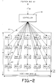
- FIG. 1 is a block diagram of a data processing system in which the invention is employed;
- FIG. 2 is a block diagram of the memory bank of the data processing system of FIG. 1;
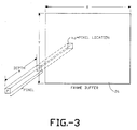
- FIG. 3 is a conceptual showing of a framebuffer represented in the memory bank of FIG. 2, and a pixel thereof;
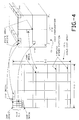
- FIG. 4 is an illustrative showing of the mapping between a memory chip bank and a conceptual framebuffer;
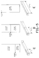
- FIG. 5 shows for three exemplary pixel depths the allocation of memory according to the invention;
- FIG. 6 shows the format of data to be transferred between the subsystem bus and memory of FIG. 1 in a first type of memory transaction, according to the invention;
- FIG. 7 shows the format of data to be transferred between the memory controller and memory of FIG. 1 in a second type of memory transaction, according to the invention;
- FIG. 8 shows a portion of a graphics subsystem according to the invention, having multiple memory banks and multiple controllers;
- FIG. 9 is a block diagram of a memory controller according to the invention; and
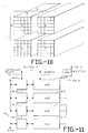
- FIGS. 10 and 11 show a particular portion of a framebuffer and a corresponding configuration of the graphics subsystem, according to an additional embodiment of the invention.
- Referring now to the drawing, and in particular to FIG. 1, a graphics subsystem 10 (memory module) is connected by
processor bus 14 toport 52 of aprocessor 50.Bus 14 is adapted to carry signals (specifying data or address) betweenprocessor 50 andsubsystem 10, and is connected tosubsystem 10 through abus interface 12. A subsystem data bus 16 (module bus) is connected tointerface 12.Graphics subsystem 10 provides a memory comprising abank 20 of K conventional two-port video RAM chips desirably arranged in an array A x B = K. Each chip (memory element) provides an equal plurality of storage locations, each location being addressable relative to the chip origin. The random access ports of the chips ofbank 20 are connected through acontroller 18 tosubsystem bus 16. The serial output ports of the chips ofbank 20 are connected at 150 tographics output circuitry 22, which is of conventional design and will not be described; signals output fromcircuitry 22 are connected to a conventional raster color display monitor, not shown. Additional banks of video RAM chips may be provided, as will be described. -
Processor 50 executes a graphic application program, details of which are not pertinent to the present invention, but which results in the specification of matter to be displayed. The images to be displayed are specified by aprocessor 50 in a relatively abstract and concise form, which cannot be directly used to control the display monitor. The representation must be converted to a suitable form, which for a raster display monitor is referred to as a framebuffer comprising an ordered array of framebuffer pixels, each corresponding to a display pixel of the display screen. Such conversion is referred to as rendering. In the graphics subsystem of FIG. 1,controller 18 functions to provide accelerated graphics rendering, as will be explained. - Still referring to FIG. 1,
interface 12 includes means for performing the usual functions of a bus interface, such as bus monitoring and support, bus protocol, as well as error detection. For the particular function of interfacing betweenbus 14 and thegraphics subsystem 10,interface 12 additionally provides means for arbitration of requests for access tomemory bank 20; timing means forcontroller 18, foroutput circuitry 22, formemory bank 20, and for the display monitor; and means for controllingsubsystem bus 16. - Memory
module addressing means 17 translates between processor addresses and memory chip bank addresses, as will be described in more detail after the memory chip bank has been described. Responsive to addresses fromprocessor 50, or to signals fromcontroller 18, addressingmeans 17 provides location address signals 27 tobank 20, and mask information signals tocontroller 18. It should be understood that although for clarity of description memory module addressing means is shown in FIG. 1, as separate frominterface 12 andcontroller 18, this arrangement is not significant. The necessary addressing functions may be provided by circuitry otherwise distributed, for example, distributed betweeninterface 12 andcontroller 18. - The memory provided by memory bank 20 (together with other video RAM banks, if provided) is allocated between storage for the graphics framebuffer, and system memory (storing, for example, programs). This allocation is not hardware dependent, but is accomplished by software. A parameter signal specifying a current memory allocation (that is, the position of the partition between framebuffer storage and system memory), is stored at 56.
Storage 56 is writable. The parameter signal may be input at 54, for example, from execution of a program byprocessor 50 or another processor, or may represent a boot parameter. Processor addressing means 58 generates addresses to system memory (in memory space) with reference to the value stored at 56; that is, the allocation of memory between framebuffer storage and system memory is known toprocessor 50. In the described embodiment, a 32-bit address is generated byprocessor 50, of which the value of bit 29 is set or not set, to specify memory space or i/o space addresses. This is an implementation detail; the distinction between addresses to the two address spaces may be made in any convenient way. - The video RAM chips of
bank 20 are disposed as a A x B = K chip array, for example, referring now to FIG. 2, in the described embodiment, a (A = 5) x (B = 4) array of K = 20chips 24, each chip 24 (identified by its chip array position as (a,b)) having an 8-bit parallel i/o path tocontroller 18. An equivalent implementation would be 40 chips each with a 4-bit parallel i/o path. Other chip array dimensions may also be employed, for example, (A = 4) x (B = 4) with an 8-bit parallel i/o path, or (A = 20) x (B = 1). The total number K of memory elements is the critical feature, since K x path width is the factor which affects the bandwidth.Controller 18 has the capability of accessing in parallel (path width) x A x B bits, or for the described embodiment, (8 x 5 x 4) = 160 bits. If additional chip banks are employed, each having a similar controller, then multiples of 160 bits can be accessed in parallel by the concurrent operation of the several controllers. - The set of corresponding locations in the K chips (a,b) specified by a location address from
module addressing means 17 comprises an addressed location array. - In a system using a raster display, the framebuffer storage (and the corresponding framebuffer, which is conceptual rather than physical) of a graphics subsystem is mapped to the display screen in terms of pixels (picture elements). The raster display screen comprises a rectangular array of X x Y display pixels (x,y). At any particular time, each display pixel displays a color specified by a color value; signals representing the bits of a digital representation of the color value are stored in the framebuffer storage at the (x,y) position of the framebuffer pixel corresponding to the display pixel. The display is refreshed by output circuitry such as
circuitry 22 in FIG. 1, which cyclically reads signals from the framebuffer storage, interprets the signals, and controls the display monitor appropriately to display corresponding colors in the display pixels, all in a manner well understood in the art. Changes in the display are made by updating the representations of color values in framebuffer storage; on the next refresh cycle these changes are represented by corresponding changes on the display screen. - Conceptually, the bits comprising a framebuffer pixel x,y (specifying the color value of the display pixel x,y) are regarded as being all stored at the pixel position in the framebuffer, which is regarded as a three dimensional construct. Referring now to the conceptual showing of FIG. 3, a
framebuffer 26 comprises an array, X framebuffer pixels across and Y framebuffer pixels vertically, corresponding to the X x Y display pixels of the display; at the specific framebuffer position (x,y) the framebuffer has n bits comprising a framebuffer pixel. The framebuffer pixel is said to have depth n. The information stored at the framebuffer pixel position may be regarded as divided into buffers, separately addressable. An intensity or I-buffer is always provided, the refresh being conducted from this buffer; additional buffers (of the same size), such as a double buffer or a Z buffer, may be provided, as well understood in the graphics art, for specific graphics applications. While the number of buffers employed may vary with the specific graphics application, and is thus a matter of software design choice, the number of bits in a buffer is a matter of hardware design choice in the particular graphics subsystem, depending on the design of the video output circuitry. If the buffer size is 8 bits, for example, and a single buffer is used, the framebuffer pixel depth n is 8; if two buffers are used, the framebuffer pixel depth n is 16. In other hardware designs, the buffer size can be chosen to be 24 (providing 8 bits each for red, blue and green information); in such a system a two-buffer pixel has a depth n of 48. Other buffer sizes may be provided. - Addressing means 17 and
controller 18 control the storage of signals in the A x Bvideo RAM chips 24 ofbank 20 in addressed array locations such that representations in the storage of certain adjacent framebuffer pixels can be accessed in parallel throughcontroller 18 responsive to a single location address relative to chip origin, supplied in parallel to all chips from addressingmeans 17. In particular, the framebuffer pixel signals are so stored that an update array of W x H pixels can be accessed in parallel, the update array being so specified that the entire X x Y framebuffer (and display) can be tiled by a plurality of such W x H update arrays having determined origins. Each update array can be identified by an array origin identifier. The dimensions W, H of the update array need not be equal to the dimensions A, B of the chip array, as will be described, but in the simplest case W = A and H = B. - The
connections 150 between the serial output ports ofchips 24 andvideo output circuitry 22 determine the mapping betweenchips 24 and the display screen; that is, the framebuffer pixels inmemory 20, as located by the mapping betweencontroller 18 andchips 24, must be serially accessed in raster order of (x,y) to refresh the display. - Referring now to Fig. 4, by way of illustration the mapping is shown between a conceptual three-dimensional framebuffer and a corresponding physical chip bank laid out on a plane. (The particular numbers employed are not those of a real graphics subsystem but have been chosen to provide a simple illustrative example.) An exemplary framebuffer 26-E has 100 framebuffer pixels (X = 10) x (Y = 10) as shown, each pixel having an exemplary depth of n = 4 bits. The signals representing the framebuffer are stored physically in chip bank 20-E comprising a (A = 5) x (B = 5) chip array (K = 25 chips), controlled by a controller (not shown) to provide 4-bit parallel access from the controller to each chip (a,b) in chip array 20-E. It is assumed that four 4-bit pixels can be stored in each chip without occupying all locations. Thus chip (a=1, b=1) of bank 20-E stores the four bits of pixel (x=1, y=1) in its first location; pixel (x=2, y=1) is stored in the corresponding first location of chip (a=2, b=1). These two pixels are in the first update array, and can be accessed in parallel because they are in different chips in the chip array and are in corresponding locations in the respective chips. However framebuffer pixel (x=1, y=6) is stored in the third location of chip (a=1, b=1) of bank 20-E, so that it cannot be accessed in parallel with pixel (x=1, y=1). It is thus seen that framebuffer 26-E is tiled by four 5x5 update arrays of framebuffer pixels having array origins at (1,1), (6,1), (1,6) and (6,6), and that the signals representing all the framebuffer pixels of an update array, stored in the graphics subsystem memory, will be concurrently accessed in parallel in a single memory transaction, specified by a single location address from addressing
means 17. In an actual graphics system of interest, many more than four update arrays are required to tile the display. The framebuffer pixels are stored in a set of contiguous storage locations within chips 24-E. - It will be seen that in the illustrative showing of Fig. 4, the chips of chips array 20-E are not completely filled by the contiguously stored signals representing the pixels of framebuffer 26-E. As shown, 8 contiguous bits are free in each chip. (This number is illustrative only.) The set of contiguous free locations from all chips of the array comprises the portion of the memory bank which is allocatable as system memory.
- The memory provided by
chip bank 20 can be conceptualized as globally divided into two portions, rather than divided chipwise into two portions as seen in Fig. 4. Referring now to Fig. 5, the global partition of the memory ofbank 20 for three different configurations C, D and E is shown. (It is assumed that the total memory remains constant, that is, the number of memory chips remains constant.) In configuration C, requiring a framebuffer pixel depth of n1 (for example, only an I buffer of N1 bits) the memory-i/o partition allocates a major portion of the memory to system memory. In configuration D, the framebuffer pixel depth n2 is 2 x n1, reflecting for example use of a double buffer in addition to the I buffer; only one half of the memory is allocated to system memory. In configuration E, the entire memory is required for storage of the framebuffer (pixel depth n3 = 2 x n2). For configuration E, additional system memory must be provided on another board. Fig. 5 illustrates the fact that framebuffer pixel depth is an integral multiple of buffer size; correspondingly, the memory provided bychip bank 20 is partitioned on a buffer boundary. The parameter stored in storage means 56 ofprocessor 50 specifies the position of the memory-i/o partition. The parameter stored at 56 can be rewritten, corresponding to a change in the allocation ofmemory 20; such allocation is therefore software configurable. - Additional banks of memory may be employed in the graphics subsystem, each with its controller. These additional chip arrays and controllers can be configured to support parallel update of overlapping arrays, or to support update arrays larger than each chip array.
- An example of overlapping arrays is shown in Fig. 8. Three 5x4 chip arrays are employed, each with a controller: array 20-R stores 8-bit signals for control of the red gun of the display, array 20-G stores 8-bit signals for control of the green gun, and array 20-B stores 8-bit signals for control of the blue gun. The signals stored in 20-R, 20-G, and 20-B together comprise the representation of the framebuffer. The connections 150-8 between the chip arrays and the output circuitry 22-8 are such that the bits stored in corresponding locations in 20-R, 20-B, and 20-G are serially accessed by
circuitry 22 for a single pixel address (x,y); circuitry 22-8 is adapted to support a 24-bit pixel. This implementation therefore provides a pixel depth of 24 bits, while the update array dimensions (W=5) x (H=5) are the same as the chip array dimensions (A=5 x (B=5). Each chip bank is controlled by a controller likecontroller 18 of Figs. 1 and 9. Arrays 20-R, 20-G and 20-B together comprise the subsystem memory. In this system, it is possible to update 3 x 160 or 480 bits in parallel in a single memory transaction. - An example in which the update array is larger than the chip array is shown in Fig. 10 and Fig. 11. A framebuffer update array of W x H pixels is shown, where W = 2A and H = 2B. The update array comprises four regions P, Q, S and T. The corresponding chip arrays and controllers are shown in Fig. 11. Each controller 18-P, 18-Q, 18-S, 18-T controls a bank of A x B chips. The connections 150-11 between chips 20-P, 20-Q, 20-S and 20-T and output circuitry 22-11 are such that the bits stored in corresponding locations in the four chip arrays are serially accessed by circuitry 22-11 as W x H pixels. Thus an update array larger than the chip array size is supported in this embodiment.
- Referring to Fig. 9,
controller 18 providesstate machines 100 for controlling the state of the controller;state machines 100 receive timing signals frominterface 12 onlines 80.State machines 100 output a memory cycle REQUEST semaphore online 82 to interface 12, and receive a GRANT semaphore on 81 frominterface 12.Controller 18 further provides read/write enable generating means 102, which outputs to each ofchips 24 ofbank 20 read/write enable signals onlines 88, responsive to a processor write operation or in the course of a controller graphics operation. In the described embodiment having a (A = 5) x (B = 4)chip bank 20 with 8-bit parallel paths, data is transmitted on 40-bitparallel path 84 betweencontroller 18 andsubsystem bus 16; data is transmitted on 160-bitparallel path 86 betweencontroller 18 andmemory bank 20. - For each memory chip of
bank 20,controller 18 provides an internal processor for the execution of atomic graphics operations, theprocessors 104 operating in parallel. Such atomic graphics operations include, for example, writing a geometrical figure to the framebuffer, moving a figure from one part of the framebuffer to another part, drawing a line, and the like. The details of such atomic graphics operations are not pertinent to the present invention.Controller 18 further provides signal multiplexing/demultiplexing means 106 for controlling the transfer of signals betweenmemory bank 20 andsubsystem bus 16, and receives from module addressing means 17 mask information signals on 92 for the control ofmultiplexers 106.Controller 18 provides to module addressing means 17 address request signals on 94, to be described. - In multi-controller embodiments such as that shown in Fig. 11, each controller is initialized with initializing signals specifying the size of the update array (values of W and H) and the position in the update array of the pixels stored in the chip bank managed by the controller. Such initializing signals are stored at 107 (Fig. 9). As described below, all data signals for atomic graphics operations are provided in common to all controllers; each controller interprets the data uniquely with respect to its stored initializing signals. For processor read/write operations, either of system memory of the framebuffer storage, a controller
select signal 95 is output tostate machines 100 frommodule addressing means 17. - Every access to the graphics
subsystem memory bank 20 is carried out throughcontroller 18; all memory transactions are carried out as array access transactions. Three modes of memory transaction are provided; processor system memory operation, processor read/write framebuffer operation, and controller atomic graphics operation.Interface 12 arbitrates among requests for these three kinds of access tomemory bank 20. System memory (highest priority) and processor read/write framebuffer (next highest priority) operations are induced byprocessor 50. Atomic graphics transactions, although performed responsive to data transmitted fromprocessor 50, must be requested by controller 18 (cycle request, on line 82). In response to the CYCLE REQUEST semaphore, if no operation having either of the two higher priorities is pending,interface 12 asserts the GRANT signal (on line 81) tocontroller 18. In the absence of the GRANT signal, theprocessors 104 ofcontroller 18 are not enabled, so thatcontroller 18 functions only as a multiplexer; when the GRANT signal is provided, theprocessors 104 ofcontroller 18 are enabled. - A system memory access will be first described. In a system memory operation,
processor 50 reads or writes locations in the portion ofchip array 20 which is allocated as system memory. In the described embodiment, data which is the subject of system memory transactions is cacheable and must be ECC protected. - To carry out a system memory operation in the described embodiment,
processor 50 through its addressingmeans 58, and with reference to the signal stored at 56, addresses memory space, placing signals representative of the memory space address onbus 14 in a first operating cycle. For a write operation, during each of the next fourcycles processor 50places 32 bits (4 bytes) of write data signals onbus 14, comprising in four cycles a 128-bit "octoword"; for a read operation, no data signals are placed onbus 14 byprocessor 50. -
Interface chip 12 recognizes the address as a memory space address by means of the address bit 29, and gives priority to this operation by deasserting the GRANT signal on 81. Memorymodule addressing means 17 responds to the processor memory space address signals by providing location address signals which are input tomemory bank 20, and (in a multicontroller system like that of Fig. 8 or Fig. 11) a controllerselect signal 95. The selected controller recognizes the controller select signal; other controllers, if present, are inactive. - In a write operation, in the four cycles after transmission of the memory address from
processor 50, the write data signals fromprocessor 50 are received byinterface 12.Interface 12 generates ECC data and transmits the data signals in the form of four words, each comprising 8 bits of ECC data and 32 bits of write data (4 bytes), onsubsystem bus 16.Multiplexers 106 of the selected controller are controlled bystate machines 100 to store the four successively transmitted write data words; write enable signal is provided on 88 to all K chips; the four write words are then in a single operation written by selectedcontroller 18 to the locations in the portion of memory allocated to system memory, specified by the location address from addressingmeans 17. Referring to Fig. 6, the format of data transferred in this memory transaction is shown schematically. It will be seen that the 4-word unit is stored aligned with the chip array origin. - Words, 0, 1, 2, and 3 are transferred in successive cycles to/from
bus 16; the four words are transferred in parallel to/frommemory 20 in a single transaction. In a read operation,controller 18 reads the four words frommemory 20 during a single memory transaction, and then during each of four sequential cycles multiplexes one of the four words ontobus 16 to transmit them in the appropriate order toprocessor 50. In a write operation,controller 18 receives the four words frombus 16 during four sequential cycles, and thereafter transfers the four words in parallel tomemory 20 in a single memory transaction. - Memory operations of the kind described do not appear to
processor 50 to be in any way different from references to conventional system memory. - A second mode of memory access is an access required for an "atomic graphics operation" resulting in the update of an array of pixels in the framebuffer. Such memory access has the lowest priority of the three modes. An atomic graphics operation may be, for example, writing a polygon to the framebuffer. Generally, the polygon is tiled by a plurality of update arrays, requiring a corresponding number of memory accesses to complete the writing operation. Such accesses proceed so long as the GRANT semaphore from
interface 12 is asserted; if a higher-priority memory transaction is requested byprocessor 50, the GRANT semaphore is deasserted, interrupting the graphics operation. - To initiate an atomic graphics operation,
processor 50 addresses subsystem 10 with an i/o space address, and places data signals onbus 14, specifying operation data such as the x,y positions in the framebuffer of the vertices of a polygon to be drawn.Interface 12 transmits the operation data signals onsubsystem bus 16. The controllers (if more than one is employed) all receive the same operation data signals. (In a multiprocessor environment, before the processor can transmit such data signals, it must execute a "controller acquire" operation to ascertain whether the controller is executing an operation for another processor.) - Each controller which supports a chip array into which the polygon is to be written sends the CYCLE REQUEST semaphore to interface 12; if no higher priority operations are pending,
interface 12 asserts the GRANT line.Controller 18 identifies the first update array to be accessed in the graphics operation, and issues address request signals tomodule addressing means 17, which outputs a corresponding location address to chipbank 20. As controlled bystate machines 100, theprocessors 104 of each controller execute the graphics operation in parallel with respect to the operation data; write enable generator means 102 provides an enable signal tochips 24. All pixels in the addressed update array are accessed in parallel; however, not all pixel values may be changed in any particular update operation. Repeated array accesses may be required to complete the operation; in thiscase controller 18 provides further address request signals to addressingmeans 17, specifying the next update array to be accessed. Responsive to the address request signal, means 17 provides the next location address signals tomemory 20. - It will be seen that this mode of operation makes efficient use of the increased memory bandwidth provided. In a single memory transaction, a relatively large number of bits is accessed and can be updated, by means of rendering operations that are highly parallel in nature.
- A third mode of operation is also provided, for carrying out graphics operations which are not well suited to the class of operations carried out by
controller 18. Such operations are best executed by havingprocessor 50 read and write specific pixels in the framebuffer. In this case, addressing means 58 ofprocessor 50 generates an i/o space address, specifying a specific framebuffer pixel (x,y) to be placed onbus 14. Such processor framebuffer address is distinguished as a processor framebuffer read/write address (from framebuffer addresses transmitted as part of atomic graphics operation commands) in any convenient way, for example, by transmission of a read or write instruction. For a write pixel operation, in thenext cycle processor 50 places write data signals onbus 14.Interface 12 recognizes the i/o address as specifying a high priority memory module operation, and deasserts GRANT. Memorymodule addressing means 17 responds to the processor i/o address by providing an address expressed as a location address (specifying update array origin) transmitted at 27 tomemory bank 20, and mask information signals (specifying offset within the array) transmitted at 92 todemultiplexers 106 ofcontroller 18. - In a processor write to the framebuffer, write data signals are transmitted on
module bus 16. As controlled bystate machines 100,controller 18 accesses in parallel all pixels in the identified update array specified by the location address; themultiplexers 106, responsive to mask information input at 92, multiplex the write data signals into the particular location specified by the offset.Processor 50 may read a selected pixel in a similar manner. - From this description it is evident that in all modes of
operation controller 18 always accesses in parallel an array of storage locations inmemory 20 specified by a location address relative to chip origin, even in cases (as whenprocessor 50 reads or writes one pixel) where fewer than all the locations are of interest. - Data to be stored in system memory is desirably ECC protected, whereas framebuffer data is generally not so protected. In the described embodiment, a (A = 5 x B = 4) chip array is therefore particularly convenient for flexible partitioning between system memory and framebuffer memory, as four 4-byte words each with a byte of ECC data fit exactly into the chip array, while a (W = 5 x H = 4) update array is conveniently supported by the same chip array. However, other chip array dimensions may be appropriate in particular implementations, in which write and ECC data are formatted differently.
- The memory architecture of the present invention is particularly advantageous for a data processing system which is commercially provided in a number of configurations, as the simplest system need have only a single memory board, providing both system and framebuffer memory. Such a system is relatively economical for the graphics performance which is obtained. As additional memory is added to the system, no hardware change is required to reallocate the memory of the original memory board to be entirely dedicated to framebuffer memory, if desired. Reallocation of memory upon application changes is also made easy by the present invention.
Claims (7)
- A data processing system, comprising:
a data processing unit (50);
a memory module (20);
partition means (56), coupled to said data processing unit, for storing a boundary address value;and
a graphics subsystem (10), coupled to said data processing unit;
characterized by:
said memory module (20) including an array of K simultaneously accessible memory elements (24), each memory element storing a multiplicity of data values at specified address locations within a predefined address space, said predefined address space being divided into two portions including a graphics address space and a system memory address space, wherein K is an integer having a value of at least four;
said boundary address value stored in said partition means denoting a boundary between said graphics address space and said system memory address space;
said graphics subsystem (10) including:
a set of K parallel graphics processors (104), coupled to said data processing unit and said memory module, for storing and updating pixel values specifying pixels (x,y) of an X x Y raster framebuffer (26) in said graphics address space of said memory module, said set of K parallel graphics processors (104) coupled to said K memory elements (24) for concurrently accessing and updating an update array of K pixel values, said framebuffer being sequentlally addressable as a plurality of update arrays which tile the framebuffer, including a plurality of horizontal rows of update arrays forming an array of said update arrays; and
system memory access means (12, 17, 18) for reading and storing data in specified address locations in said system memory address space of said memory module and for transmitting said read and stored data to and from said data processing unit;
wherein each of said K memory elements stores a multiplicity of data values at locations in said graphics address space and a multiplicity of data values in locations in said system memory address space. - A data processing system as set forth in claim 1, further characterized by:
said data processing unit (50) including means for sending commands to said graphics subsystem (10), said commands including system memory access commands and graphics commands;
said graphics subsystem (10) including interface means (12), coupled to said data processing unit (50), said graphics processors and said system memory access means, for receiving commands from said data processing unit, transferring graphics commands to said graphics subsystem, and transferring system memory access commands to said system memory access means. - A data processing system as set forth in claim 1 or 2, further characterized by:
said graphics address space and said system memory address space having sizes defined by said boundary address value stored in said partition means (56); said data processing unit (50) including means for changing said boundary address value stored in said partition means and thereby changing said address space sizes of said graphics address space and said system memory address space. - A data processing system as set forth in claim 1, further characterized by:
said graphics subsystem (10) including output circuitry (22) for accessing said X x Y raster framebuffer (26) in said graphics address space of said memory module and outputting corresponding display control signals to a display device. - A method of operating a data processing system having a data processing unit (50); a memory module (20), partition means (56), coupled to said data processing unit, for storing a boundary address value, and a graphics subsystem (10), coupled to said data processing unit; said method comprising:
storing graphics data in said memory module; and
accessing said graphics data in said memory module and outputting corresponding display control signals to a display device;
characterized by:
providing said memory module (20) as an array of K -simultaneously accessible memory elements (24), each memory element storing a multiplicity of data values at specified address locations within a predefined address space, wherein K is an integer having a value of at least four;
partitioning said predefined address space into two portions, including a graphics address space and a system memory address space, by storing in said partition means said boundary address value denoting a boundary between said graphics address space and said system memory address space;
providing in said graphics subsystem (10) a set of K parallel graphics processors (104), coupled to said data processing unit and K memory elements (24), for storing and updating pixel values specifying pixels (x,y) of an X x Y raster framebuffer (26) in said graphics address space of said memory module; said framebuffer being sequentially addressable as a plurality of update arrays which tile the framebuffer, including a plurality of horizontal rows of update arrays forming an array of said update arrays;
said set of K parallel graphics processors (104) coupled to said K memory elements (24) concurrently accessing and updating an update array of K pixel values; and
reading and storing data in specified address locations in said system memory address space of said memory module and transmitting said read and stored data to and from said data processing unit;
wherein each of said K memory elements stores a multiplicity of data values at locations in said graphics address space and a multiplicity of data values in locations in said system memory address space. - The method of claim 5, further characterized by:
said data processing unit (50) sending commands to said graphics subsystem (10), said commands including system memory access commands and graphics commands;
said graphics subsystem (10) receiving said commands from said data processing unit, transferring said graphics commands to said graphics subsystem, and responding to system memory access commands by reading and storing data in specified address locations in said system memory address space of said memory module and transmitting said read and stored data to and from said data processing unit. - The method of claim 5 or 6, further characterized by:
said graphics address space and said system memory address space having sizes defined by said boundary address value stored in said partition means (56):
changing said boundary address value stored in said partition means and thereby changing said address space sizes of said graphics address space and said system memory address space.
Applications Claiming Priority (2)
| Application Number | Priority Date | Filing Date | Title |
|---|---|---|---|
| US07/124,897 US4953101A (en) | 1987-11-24 | 1987-11-24 | Software configurable memory architecture for data processing system having graphics capability |
| US124897 | 1987-11-24 |
Publications (3)
| Publication Number | Publication Date |
|---|---|
| EP0318259A2 EP0318259A2 (en) | 1989-05-31 |
| EP0318259A3 EP0318259A3 (en) | 1991-07-24 |
| EP0318259B1 true EP0318259B1 (en) | 1995-02-08 |
Family
ID=22417328
Family Applications (1)
| Application Number | Title | Priority Date | Filing Date |
|---|---|---|---|
| EP88311067A Expired - Lifetime EP0318259B1 (en) | 1987-11-24 | 1988-11-23 | Software configurable memory architecture for data processing system having graphics capability |
Country Status (5)
| Country | Link |
|---|---|
| US (1) | US4953101A (en) |
| EP (1) | EP0318259B1 (en) |
| JP (1) | JP2683564B2 (en) |
| CA (1) | CA1312963C (en) |
| DE (1) | DE3852989T2 (en) |
Families Citing this family (38)
| Publication number | Priority date | Publication date | Assignee | Title |
|---|---|---|---|---|
| US5287450A (en) * | 1988-09-29 | 1994-02-15 | Mitsubishi Denki Kabushiki Kaisha | Video signal brancher |
| US5197140A (en) * | 1989-11-17 | 1993-03-23 | Texas Instruments Incorporated | Sliced addressing multi-processor and method of operation |
| US5218678A (en) * | 1989-11-17 | 1993-06-08 | Digital Equipment Corporation | System and method for atomic access to an input/output device with direct memory access |
| US5287452A (en) * | 1990-03-23 | 1994-02-15 | Eastman Kodak Company | Bus caching computer display system |
| JP3350043B2 (en) | 1990-07-27 | 2002-11-25 | 株式会社日立製作所 | Graphic processing apparatus and graphic processing method |
| DE69132796T2 (en) * | 1990-11-30 | 2002-04-25 | Sun Microsystems Inc | METHOD AND DEVICE FOR REPRESENTING GRAPHIC IMAGES |
| CA2070934C (en) * | 1992-06-10 | 1998-05-05 | Benny Chi Wah Lau | Graphics display system |
| US5404448A (en) * | 1992-08-12 | 1995-04-04 | International Business Machines Corporation | Multi-pixel access memory system |
| US5404437A (en) * | 1992-11-10 | 1995-04-04 | Sigma Designs, Inc. | Mixing of computer graphics and animation sequences |
| US6116768A (en) * | 1993-11-30 | 2000-09-12 | Texas Instruments Incorporated | Three input arithmetic logic unit with barrel rotator |
| KR960706657A (en) * | 1993-11-30 | 1996-12-09 | 토마스 씨. 토코스 | METHOD AND APPARATUS FOR PROVIDING AND MAXIMIZING CONCURRENT OPERATIONS IN A SHARED MEMORY SYSTEM |
| WO1995015528A1 (en) * | 1993-11-30 | 1995-06-08 | Vlsi Technology, Inc. | A reallocatable memory subsystem enabling transparent transfer of memory function during upgrade |
| US5598576A (en) * | 1994-03-30 | 1997-01-28 | Sigma Designs, Incorporated | Audio output device having digital signal processor for responding to commands issued by processor by emulating designated functions according to common command interface |
| US5515107A (en) * | 1994-03-30 | 1996-05-07 | Sigma Designs, Incorporated | Method of encoding a stream of motion picture data |
| US5528309A (en) | 1994-06-28 | 1996-06-18 | Sigma Designs, Incorporated | Analog video chromakey mixer |
| TW399189B (en) * | 1994-10-13 | 2000-07-21 | Yamaha Corp | Control device for the image display |
| US5513318A (en) * | 1994-12-28 | 1996-04-30 | At&T Corp. | Method for built-in self-testing of ring-address FIFOs |
| US5790881A (en) * | 1995-02-07 | 1998-08-04 | Sigma Designs, Inc. | Computer system including coprocessor devices simulating memory interfaces |
| TW335466B (en) * | 1995-02-28 | 1998-07-01 | Hitachi Ltd | Data processor and shade processor |
| US5767866A (en) * | 1995-06-07 | 1998-06-16 | Seiko Epson Corporation | Computer system with efficient DRAM access |
| US6204864B1 (en) | 1995-06-07 | 2001-03-20 | Seiko Epson Corporation | Apparatus and method having improved memory controller request handler |
| US5872998A (en) * | 1995-11-21 | 1999-02-16 | Seiko Epson Corporation | System using a primary bridge to recapture shared portion of a peripheral memory of a peripheral device to provide plug and play capability |
| US5719511A (en) * | 1996-01-31 | 1998-02-17 | Sigma Designs, Inc. | Circuit for generating an output signal synchronized to an input signal |
| US5748203A (en) * | 1996-03-04 | 1998-05-05 | United Microelectronics Corporation | Computer system architecture that incorporates display memory into system memory |
| US6128726A (en) | 1996-06-04 | 2000-10-03 | Sigma Designs, Inc. | Accurate high speed digital signal processor |
| US5818468A (en) * | 1996-06-04 | 1998-10-06 | Sigma Designs, Inc. | Decoding video signals at high speed using a memory buffer |
| US6940496B1 (en) * | 1998-06-04 | 2005-09-06 | Silicon, Image, Inc. | Display module driving system and digital to analog converter for driving display |
| US6145033A (en) * | 1998-07-17 | 2000-11-07 | Seiko Epson Corporation | Management of display FIFO requests for DRAM access wherein low priority requests are initiated when FIFO level is below/equal to high threshold value |
| US6119207A (en) * | 1998-08-20 | 2000-09-12 | Seiko Epson Corporation | Low priority FIFO request assignment for DRAM access |
| US6819321B1 (en) * | 2000-03-31 | 2004-11-16 | Intel Corporation | Method and apparatus for processing 2D operations in a tiled graphics architecture |
| US6611469B2 (en) | 2001-12-11 | 2003-08-26 | Texas Instruments Incorporated | Asynchronous FIFO memory having built-in self test logic |
| US20060177122A1 (en) * | 2005-02-07 | 2006-08-10 | Sony Computer Entertainment Inc. | Method and apparatus for particle manipulation using graphics processing |
| US7627723B1 (en) * | 2006-09-21 | 2009-12-01 | Nvidia Corporation | Atomic memory operators in a parallel processor |
| US9513905B2 (en) * | 2008-03-28 | 2016-12-06 | Intel Corporation | Vector instructions to enable efficient synchronization and parallel reduction operations |
| US8688957B2 (en) | 2010-12-21 | 2014-04-01 | Intel Corporation | Mechanism for conflict detection using SIMD |
| US9411592B2 (en) | 2012-12-29 | 2016-08-09 | Intel Corporation | Vector address conflict resolution with vector population count functionality |
| US9411584B2 (en) | 2012-12-29 | 2016-08-09 | Intel Corporation | Methods, apparatus, instructions, and logic to provide vector address conflict detection functionality |
| EP3565259A1 (en) * | 2016-12-28 | 2019-11-06 | Panasonic Intellectual Property Corporation of America | Three-dimensional model distribution method, three-dimensional model receiving method, three-dimensional model distribution device, and three-dimensional model receiving device |
Family Cites Families (8)
| Publication number | Priority date | Publication date | Assignee | Title |
|---|---|---|---|---|
| US3328768A (en) * | 1964-04-06 | 1967-06-27 | Ibm | Storage protection systems |
| US4197590A (en) * | 1976-01-19 | 1980-04-08 | Nugraphics, Inc. | Method for dynamically viewing image elements stored in a random access memory array |
| US4092728A (en) * | 1976-11-29 | 1978-05-30 | Rca Corporation | Parallel access memory system |
| US4432067A (en) * | 1981-05-07 | 1984-02-14 | Atari, Inc. | Memory cartridge for video game system |
| US4608632A (en) * | 1983-08-12 | 1986-08-26 | International Business Machines Corporation | Memory paging system in a microcomputer |
| CA1240427A (en) * | 1984-03-28 | 1988-08-09 | Kabushiki Kaisha Toshiba | Memory control apparatus for a crt controller |
| DE3684309D1 (en) * | 1986-05-06 | 1992-04-16 | Digital Equipment Corp | MULTI-PORT STORAGE AND SOURCE DEVICE FOR IMAGE POINT INFORMATION. |
| US4773044A (en) * | 1986-11-21 | 1988-09-20 | Advanced Micro Devices, Inc | Array-word-organized display memory and address generator with time-multiplexed address bus |
-
1987
- 1987-11-24 US US07/124,897 patent/US4953101A/en not_active Expired - Lifetime
-
1988
- 1988-11-23 CA CA000583846A patent/CA1312963C/en not_active Expired - Fee Related
- 1988-11-23 DE DE3852989T patent/DE3852989T2/en not_active Expired - Fee Related
- 1988-11-23 EP EP88311067A patent/EP0318259B1/en not_active Expired - Lifetime
- 1988-11-24 JP JP63297175A patent/JP2683564B2/en not_active Expired - Fee Related
Also Published As
| Publication number | Publication date |
|---|---|
| DE3852989D1 (en) | 1995-03-23 |
| DE3852989T2 (en) | 1995-10-12 |
| JP2683564B2 (en) | 1997-12-03 |
| US4953101A (en) | 1990-08-28 |
| EP0318259A2 (en) | 1989-05-31 |
| CA1312963C (en) | 1993-01-19 |
| EP0318259A3 (en) | 1991-07-24 |
| JPH01302442A (en) | 1989-12-06 |
Similar Documents
| Publication | Publication Date | Title |
|---|---|---|
| EP0318259B1 (en) | Software configurable memory architecture for data processing system having graphics capability | |
| US4704697A (en) | Multiple station video memory | |
| US4991110A (en) | Graphics processor with staggered memory timing | |
| US5909225A (en) | Frame buffer cache for graphics applications | |
| EP0447225B1 (en) | Methods and apparatus for maximizing column address coherency for serial and random port accesses in a frame buffer graphics system | |
| US6104418A (en) | Method and system for improved memory interface during image rendering | |
| US5025249A (en) | Pixel lookup in multiple variably-sized hardware virtual colormaps in a computer video graphics system | |
| US4745407A (en) | Memory organization apparatus and method | |
| US5251298A (en) | Method and apparatus for auxiliary pixel color management using monomap addresses which map to color pixel addresses | |
| US5666521A (en) | Method and apparatus for performing bit block transfers in a computer system | |
| US4782462A (en) | Raster scan video controller with programmable prioritized sharing of display memory between update and display processes and programmable memory access termination | |
| JP3639464B2 (en) | Information processing system | |
| KR100227133B1 (en) | A memory architecture using conserved addressing and systems and methods using the same | |
| JP2001505342A (en) | Computer system controller with internal memory and external memory control | |
| EP0398510B1 (en) | Video random access memory | |
| JPH0690613B2 (en) | Display controller | |
| US5216413A (en) | Apparatus and method for specifying windows with priority ordered rectangles in a computer video graphics system | |
| US4845663A (en) | Image processor with free flow pipeline bus | |
| US4675842A (en) | Apparatus for the display and storage of television picture information by using a memory accessible from a computer | |
| EP0182454B1 (en) | Video system controller with a row address override circuit | |
| US4935880A (en) | Method of tiling a figure in graphics rendering system | |
| EP0752694B1 (en) | Method for quickly painting and copying shallow pixels on a deep frame buffer | |
| EP0244112A2 (en) | A method and apparatus for addressing video rams and refreshing a video monitor with a variable resolution | |
| JPH0687189B2 (en) | Display device | |
| US5396263A (en) | Window dependent pixel datatypes in a computer video graphics system |
Legal Events
| Date | Code | Title | Description |
|---|---|---|---|
| PUAI | Public reference made under article 153(3) epc to a published international application that has entered the european phase |
Free format text: ORIGINAL CODE: 0009012 |
|
| AK | Designated contracting states |
Kind code of ref document: A2 Designated state(s): DE FR GB |
|
| PUAL | Search report despatched |
Free format text: ORIGINAL CODE: 0009013 |
|
| AK | Designated contracting states |
Kind code of ref document: A3 Designated state(s): DE FR GB |
|
| 17P | Request for examination filed |
Effective date: 19911018 |
|
| 17Q | First examination report despatched |
Effective date: 19930419 |
|
| GRAA | (expected) grant |
Free format text: ORIGINAL CODE: 0009210 |
|
| AK | Designated contracting states |
Kind code of ref document: B1 Designated state(s): DE FR GB |
|
| REF | Corresponds to: |
Ref document number: 3852989 Country of ref document: DE Date of ref document: 19950323 |
|
| ET | Fr: translation filed | ||
| PLBE | No opposition filed within time limit |
Free format text: ORIGINAL CODE: 0009261 |
|
| STAA | Information on the status of an ep patent application or granted ep patent |
Free format text: STATUS: NO OPPOSITION FILED WITHIN TIME LIMIT |
|
| 26N | No opposition filed | ||
| REG | Reference to a national code |
Ref country code: GB Ref legal event code: 732E |
|
| REG | Reference to a national code |
Ref country code: GB Ref legal event code: IF02 |
|
| REG | Reference to a national code |
Ref country code: GB Ref legal event code: 732E |
|
| PGFP | Annual fee paid to national office [announced via postgrant information from national office to epo] |
Ref country code: GB Payment date: 20070125 Year of fee payment: 19 |
|
| PGFP | Annual fee paid to national office [announced via postgrant information from national office to epo] |
Ref country code: DE Payment date: 20070228 Year of fee payment: 19 |
|
| PGFP | Annual fee paid to national office [announced via postgrant information from national office to epo] |
Ref country code: FR Payment date: 20070207 Year of fee payment: 19 |
|
| GBPC | Gb: european patent ceased through non-payment of renewal fee |
Effective date: 20071123 |
|
| PG25 | Lapsed in a contracting state [announced via postgrant information from national office to epo] |
Ref country code: DE Free format text: LAPSE BECAUSE OF NON-PAYMENT OF DUE FEES Effective date: 20080603 |
|
| REG | Reference to a national code |
Ref country code: FR Ref legal event code: ST Effective date: 20080930 |
|
| PG25 | Lapsed in a contracting state [announced via postgrant information from national office to epo] |
Ref country code: GB Free format text: LAPSE BECAUSE OF NON-PAYMENT OF DUE FEES Effective date: 20071123 |
|
| PG25 | Lapsed in a contracting state [announced via postgrant information from national office to epo] |
Ref country code: FR Free format text: LAPSE BECAUSE OF NON-PAYMENT OF DUE FEES Effective date: 20071130 |