EP0316147A2 - Treiberschaltung und -verfahren mit hoher Verstärkung - Google Patents
Treiberschaltung und -verfahren mit hoher Verstärkung Download PDFInfo
- Publication number
- EP0316147A2 EP0316147A2 EP88310525A EP88310525A EP0316147A2 EP 0316147 A2 EP0316147 A2 EP 0316147A2 EP 88310525 A EP88310525 A EP 88310525A EP 88310525 A EP88310525 A EP 88310525A EP 0316147 A2 EP0316147 A2 EP 0316147A2
- Authority
- EP
- European Patent Office
- Prior art keywords
- coupled
- current
- transistor
- circuit
- collector
- Prior art date
- Legal status (The legal status is an assumption and is not a legal conclusion. Google has not performed a legal analysis and makes no representation as to the accuracy of the status listed.)
- Granted
Links
Images

Classifications
-
- G—PHYSICS
- G05—CONTROLLING; REGULATING
- G05F—SYSTEMS FOR REGULATING ELECTRIC OR MAGNETIC VARIABLES
- G05F3/00—Non-retroactive systems for regulating electric variables by using an uncontrolled element, or an uncontrolled combination of elements, such element or such combination having self-regulating properties
- G05F3/02—Regulating voltage or current
- G05F3/08—Regulating voltage or current wherein the variable is DC
- G05F3/10—Regulating voltage or current wherein the variable is DC using uncontrolled devices with non-linear characteristics
- G05F3/16—Regulating voltage or current wherein the variable is DC using uncontrolled devices with non-linear characteristics being semiconductor devices
- G05F3/20—Regulating voltage or current wherein the variable is DC using uncontrolled devices with non-linear characteristics being semiconductor devices using diode- transistor combinations
- G05F3/26—Current mirrors
- G05F3/265—Current mirrors using bipolar transistors only
-
- G—PHYSICS
- G05—CONTROLLING; REGULATING
- G05F—SYSTEMS FOR REGULATING ELECTRIC OR MAGNETIC VARIABLES
- G05F3/00—Non-retroactive systems for regulating electric variables by using an uncontrolled element, or an uncontrolled combination of elements, such element or such combination having self-regulating properties
- G05F3/02—Regulating voltage or current
- G05F3/08—Regulating voltage or current wherein the variable is DC
- G05F3/10—Regulating voltage or current wherein the variable is DC using uncontrolled devices with non-linear characteristics
- G05F3/16—Regulating voltage or current wherein the variable is DC using uncontrolled devices with non-linear characteristics being semiconductor devices
- G05F3/20—Regulating voltage or current wherein the variable is DC using uncontrolled devices with non-linear characteristics being semiconductor devices using diode- transistor combinations
- G05F3/22—Regulating voltage or current wherein the variable is DC using uncontrolled devices with non-linear characteristics being semiconductor devices using diode- transistor combinations wherein the transistors are of the bipolar type only
Definitions
- the present invention relates to electronic circuits and more specifically, to methods and circuitry for optimizing the operating characteristics of driver designs which function efficiently and independently of loading conditions.
- Driver circuits or digital peripheral drivers may be described as interface devices which are frequently employed to switch high current, high voltage loads in response to standard digital logic input signals. Examples of such loads may include relays, solenoids, lamps, or other peripheral circuit elements.
- driver circuits While the above approach to designing driver circuits guarantees operation within the range of anticipated variations, the resulting circuits generate excessive drive currents under optimum operating conditions as well as undesirable power dissipation. Moreover, many power drivers in the past have been designed to have current ratings which are two to four times the actual load which results in even further excessive waste of current. Finally, driver circuits are typically designed to operate with a particular load. Any change of loading condition to such designs may result in undesirable operating characteristics. Namely, replacing the "designed load" with one that requires less drive current is at best inefficient, while substituting a load that requires greater drive current may render the driver insufficient. In the later situation, the driver may in fact come out of the saturated state and dissipate excessive power. This in turn may cause a thermally generated loss of functionality if the device is thermally protected and a catastrophic device failure if it is not.
- a need has arisen for a high efficiency, high gain driver circuit that is suitable for power applications.
- a need has arisen for a driver circuit that optimizes the utilization of drive current for a variety of loading conditions.
- Such a driver circuit should ideally be suitable for implementation in integrated circuit form and capable of fulfilling the need for such a design in a broad variety of applications including high power automotive and portable equipment operating environments.
- a four terminal, high efficiency, high gain driver circuit suitable for power application and which exhibits optimum operating characteristics independently of circuit loading conditions.
- This advantage and others are accomplished by providing a driver design having overcurrent limiting, a self-adjust predriver and minimal standby current.
- a startup transistor initiates a positive feedback loop that effects the turn-on of drive regulation transistors, predrive transistors, and finally a drive or output transistor.
- the drive regulation transistors are driven beyond the level required for a given load, the collector to emitter voltage of the driving transistor decreases causing the drive regulation transistors to saturate.
- the input drive to the positive feedback loop is reduced and the drive current provided by the drive regulation transistors is automatically tailored to the load.
- the drive regulation transistors in conjunction with a current splitter and current sensing resistor operate to reduce the positive feedback loop drive and limit the load current.
- control transistors In addition to initiation of circuit operation by the startup transistor, the control transistors together with the start-up transistor and control resistor provide a means to disable the positive feedback loop in the absence of a source of current to the control pin. Furthermore current supplied from the current splitter is available to assist in driving the control transistors in the event that it is desirable to turn the driving circuit off from a conducting condition. Finally, by providing current to the control input, positive feedback loop operation is initiated by the start-up transistor as described above.
- the driver circuit of the present invention is suitable for both low and high side driver applications.
- the circuit will provide a source of current to any load while in low side system designs the same circuit may be driven by any load. It is therefore possible to implement the driver circuit in a very broad range of applications.
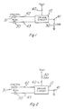
- FIG. 1 there is shown a block diagram of the four terminal driver circuit including the external bias arrangement for a high side driver application.
- current sources 30 and 31 provide the current necessary to enable the driver circuit by activating an appropriate startup transistor.
- Terminal 40 labeled VBAT is coupled to a suitable source of supply voltage.
- this terminal may be connected to the battery voltage supply.
- Terminal 41 is connected to the load 50 which may be, for example, a lamp or any electrical device requiring current drive.
- driver circuit 10 provides the necessary current source to meet the operational requirements of the load device.
- driver circuit 10 provides the same features and advantages that are present in the high side arrangement of Figure 1. It should be obvious that an immediate advantage to the design of driver circuit 10 is the ability to connect the same circuit into either high or low side applications.
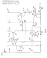
- Terminal 40 is connected to the emitter of startup PNP transistor 14 which has its base connected to the base of bias PNP transistor 15 as well as terminal 43.
- the emitter of bias transistor 15 is also connected to terminal 40.
- terminal 43 is connected to an external bias source 30.
- Terminal 43 is also connected to the collector of bias transistor 15.
- Startup transistor 14 is a dual collector transistor having a collector 35 connected to the collector 32 of multiple collector current splitter transistor 11.
- Collector 35 of startup transistor 14 is connected to the collector of a first enabling control transistor 23 and also to the base of a second enabling control transistor 22.
- the base of transistor 23 is connected to control terminal 42 and one end of resistor 45 having a second end connected to terminal 41.
- the emitter of transistor 23 is also connected to terminal 41.
- control terminal 42 is connected to a suitable source of control current 31 from external logic.
- the second collector 36 is connected to the base of a first predrive transistor 18 and the collector of transistor 22 which has an emitter connected to terminal 41.
- transistor 18 has an emitter connected to output terminal 41 as well as the emitter of a first drive regulation transistor 13.
- the collector of transistor 18 is connected to both the base and a first collector of a second predrive transistor 16 which has an emitter connected to both terminal 40 and the collector of the driving transistor 17.
- Transistor 16 has a second collector connected to the base of transistor 17.
- the base of transistor 16 is connected to one end of a resistor 48 having a second end connected to terminal 40.
- the emitter of driving transistor 17 is connected to one end of current sensing resistor 29 having a second end connected to terminal 41.
- the emitter of transistor 17 is also connected to the emitter of a second drive regulation transistor 12 which has a base connected to the bases of both transistor 13 and transistor 18.
- the base of transistor 12 is connected to the collector of transistor 13 , a second collector 33 of current splitter transistor 11, and one end of compensation capacitor 19 which has a second end connected to the collector of transistor 12.
- the collector of second drive regulation transistor 12 is also connected to the base of current splitter transistor 11 and a collector 34 of transistor 11.
- the emitter of PNP transistor 11 is connected to terminal 40.
- Circuit 10 is enabled by providing a suitable source of voltage to terminal 40, a source of current 30 to bias terminal 43, and a source of current 31 to control terminal 42.
- the load to be driven by circuit 10 may be connected between terminal 41 and system ground for the high side design.
- startup transistor 14 will turn on and provide drive current to the base of first predrive transistor 18 as well as drive regulation transistors 12 and 13.
- the first control transistor 23 turns on which in turn keeps second control transistor 22 off allowing start-up transistor 14 to adequately drive transistors 18, 13 and 12.
- drive regulation transistors 12 and 13 in conjunction with current splitter transistor 11 provide a positive feedback loop which supplies drive current to driving transistor 17 by driving the predrive transistors 16 and 18.
- start-up transistor 14 initiates the turn on of predrive transistor 18, and drive regulation transistors 12 and 13.
- Current splitter transistor 11 provides equal levels of current from collectors 33 and 34 to transistors 12 and 13; however, since transistor 12 is a larger area device, it will carry as much as four times the current of transistor 13.
- Transistor 18 may also be made larger in area than transistor 13 and functions to amplify the feedback loop current. As an example, transistor 18 may be designed to carry ten times the current carrying capacity of transistor 13.
- Capacitor 19 is coupled between the base-collector of transistor 12 and serves to reduce the high frequency loop gain to prevent unwanted oscillations.
- transistor 18 will continue to provide increased levels of drive to transistors 16 and 17. Once these devices are driven beyond the level required by a given load, their collector to emitter voltages are reduced, causing a reduction in the collector-emitter voltage of predrive transistor 18. As this voltage drops below the base-emitter voltage of transistor 18, the base current will begin to flow into the collector which in turn reduces the current drive to drive regulation transistors 12 and 13. It should be obvious that under these conditions the positive feedback loop action is diminished and the load current provided by driving transistor 17 is self-adjusted to the requirements of the load.
- transistor 12 is also turned on to provide additional current to the load through current sensing resistor 29.
- transistors 12 and 13 may be sized such that transistor 12 has a Vbe that is smaller than the Vbe of transistor 13 by, for example, a factor of four for equal collector currents.
- Current splitter transistor 11 provides equal amounts of current from collectors 33 and 34 to provide the current source for both transistors 12 and 13. Under these conditions, transistor 12 conducts a greater amount of current than transistor 13. As current begins to flow to the load from drive transistor 17 and conducting drive regulation transistor 12, a voltage drop is established across current sensing resistor 29.
- transistor 13 When this voltage drop exceeds the difference in Vbe between transistors 12 and 13, transistor 13 will increasingly conduct and divert drive current from the base of transistor 18. This results in a reduction in the base drive to transistor 16 and driving transistor 17 which regulates the output current level.
- the output current will be limited to the Vbe of transistor 13 minus the Vbe of transistor 12 divided by the resistance of current sensing resistor 29.
- Current driving circuit 10 may be conveniently disabled by the operation of control transistors 22 and 23, control resistor 45, startup transistor 14, and current splitter transistor 11.
- control transistor 23 By removing the source of current 31 to control terminal 42, control transistor 23 will be turned off.
- Control resistor 45 references the base of transistor 23 to its emitter to ensure the off condition.
- a second control transistor 22 With transistor 23 in a non-conducting state, a second control transistor 22 will turn on as base drive is provided by collector 35 of start-up transistor 14. This results in the removal of base drive from transistor 18 which inhibits feedback loop operation and disables driving circuit 10.
- collector 32 of transistor 11 Under operating conditions wherein circuit 10 was previously on, collector 32 of transistor 11 will provide additional current drive to the base of transistor 22 to ensure that the positive feedback loop is turned off.
- current source 31 is applied to control terminal 42 which turns the first control transistor 23 on and turns the second control transistor off. Circuit operation is thereafter as described above.
- circuit 10 provides only that current necessary to drive a given load and therefore exhibits optimal power supply to ground current levels as well as reduced sensitivity to power supply voltage variations. Reduced power dissipation is made possible by the fact that current driving transistor 17 is maintained in a low "ON" state.
- the current driver circuit 10 in the low side driver configuration of Figure 2.
- the circuit of Figure 3 may be externally connected as follows.
- the load 50 is connected from a source of supply voltage (Vbat) to terminal 40
- terminal 41 is connected to circuit ground
- control and bias sources 31 and 30 are respectively connected to terminals 42 and 43 as in the high side driver application described above.
- Control and operation of driver circuit 10 are as previously described for the high side application.
- the load will provide a source of current to driver circuit 10. Load current will be tailored to suit the given loading conditions as described above.
- terminal 40 is coupled to the emitter of startup transistor 14 through startup resistor 27 and also the emitter of bias transistor 15 through bias resistor 28.
- the collector-base of transistor 15 is connected to terminal 43 to which an external bias source 30 is connected during circuit operation.
- the base of transistor 15 is connected to the base of startup transistor 14 which is a dual collector PNP transistor having a first collector 36 connected to the collector of a first control transistor 23 and also a first collector 32 of dual collector transistor 11.
- Transistor 14 also has a second collector 35 connected to the collector of PNP transistor 47 and the collector of NPN transistor 21.
- Control transistor 23 has a base connected to terminal 42 and one end of a resistor 45 having a second end connected to terminal 41. During operation, terminal 42 is connected to an external current source 31.
- the collector of transistor 23 is connected to the base of a second control transistor 22 and the emitters of both control transistors 22 and 23 are connected to terminal 41.
- the collector of transistor 22 is connected to a first regulation transistor 21 having an emitter connected to terminal 41 as well as one end of current sensing resistor 29.
- the other end of current sensing resistor 29 is connected to the emitter of a second regulation transistor 20 as well as the emitters of transistor 49, predrive transistor 18 and driving transistor 17.
- the base of transistor 20 is connected to its collector, to the collector of transistor 46, and also to the base of transistor 21.
- the collector is also connected to the bases of both transistor 49 and predrive transistor 18.
- the collector of transistor 49 is connected to both the base and a second collector 34 of current source transistor 11.
- the first collector 32 is connected to both collector 36 of transistor 14 and the collector of control transistor 23.
- Transistors 11 46 and 47 all have emitters coupled to terminal 40 through a current splitter resistor 24, a gain resistor 25, and a drive resistor 26 respectively.
- predrive transistor 18 has a collector connected to the base of a second predrive transistor 16 and also to one end of a resistor 48 having a second end connected to terminal 40.
- the emitter of PNP transistor 16 is connected to terminal 40 as well as the collector of NPN driving transistor 17.
- the collector of predrive transistor 16 is connected to the base of driving transistor 17.
- circuit 10 of Figure 4 Operation of the circuit 10 of Figure 4 is similar to that of the circuit of Figure 3 and will be described for the high side driver application of Figure 1.
- the comments relating to the low side driver application for the preferred embodiment apply and will not be repeated here.
- driver circuit 10 begins by startup transistor conducting upon the application of a suitable source of supply voltage to terminal 40, and current sources to both terminals 43 and 42.
- the desired load is connected between terminal 41 and system ground.
- the first control transistor 23 is conducting which prevents the turn on of transistor 22 and allows the collector 35 of startup transistor 14 to drive the bases of both transistor 49 and 18 turning these devices on and establishing a positive feedback loop that turns on predrive transistor 16 and driving transistor 17.
- the collector to emitter output voltage of transistor 17 decreases causing predrive transistor 18 to saturate and divert base drive from transistor 49.
- bias current required from bias source 30 may be reduced and power consumption optimized. Increasing the value of resistor 28 will accomplish a reduction in the bias current level.
- regulation transistors 20 and 21 in conjunction with current sensing resistor 29 operate to regulate the output current.
- Transistor 20 may, for instance, be designed to have a larger area than transistor 21 and initially will conduct a larger amount of current.
- Transistors 46 and 47 provide a source of current to the collectors of transistors 20 and 21 which operate to increase feedback loop gain and circuit response time. As the voltage drop across current sensing resistor 29 increases, transistor 21 conducts greater amounts of current and diverts base drive from the positive feedback loop described above. As a result, current is limited to a desirable level.
- control transistors 22 and 23 to enable circuit 10 is the same as described in the description of the preferred embodiment of Figure 3 and will not be repeated. It is noted that again it is not necessary to apply a source of current to control terminal 42 to disable the driver circuit and standby current is minimal. Furthermore, current supplied from the collector 34 of transistor 11 is available to assist in driving the base of transistor 22 in the event that it is desirable to turn the driving circuit off from a conducting condition.
Landscapes
- Engineering & Computer Science (AREA)
- Microelectronics & Electronic Packaging (AREA)
- Physics & Mathematics (AREA)
- Nonlinear Science (AREA)
- Electromagnetism (AREA)
- General Physics & Mathematics (AREA)
- Radar, Positioning & Navigation (AREA)
- Automation & Control Theory (AREA)
- Electronic Switches (AREA)
Applications Claiming Priority (2)
| Application Number | Priority Date | Filing Date | Title |
|---|---|---|---|
| US11871087A | 1987-11-09 | 1987-11-09 | |
| US118710 | 1987-11-09 |
Publications (3)
| Publication Number | Publication Date |
|---|---|
| EP0316147A2 true EP0316147A2 (de) | 1989-05-17 |
| EP0316147A3 EP0316147A3 (en) | 1989-06-14 |
| EP0316147B1 EP0316147B1 (de) | 1993-08-04 |
Family
ID=22380282
Family Applications (1)
| Application Number | Title | Priority Date | Filing Date |
|---|---|---|---|
| EP19880310525 Expired - Lifetime EP0316147B1 (de) | 1987-11-09 | 1988-11-09 | Treiberschaltung und -verfahren mit hoher Verstärkung |
Country Status (2)
| Country | Link |
|---|---|
| EP (1) | EP0316147B1 (de) |
| DE (1) | DE3882909T2 (de) |
Family Cites Families (4)
| Publication number | Priority date | Publication date | Assignee | Title |
|---|---|---|---|---|
| US3629691A (en) * | 1970-07-13 | 1971-12-21 | Rca Corp | Current source |
| US4085359A (en) * | 1976-02-03 | 1978-04-18 | Rca Corporation | Self-starting amplifier circuit |
| US4338646A (en) * | 1981-04-27 | 1982-07-06 | Motorola, Inc. | Current limiting circuit |
| NL8301186A (nl) * | 1983-04-05 | 1984-11-01 | Philips Nv | Stroomstabilisatieschakeling. |
-
1988
- 1988-11-09 DE DE19883882909 patent/DE3882909T2/de not_active Expired - Fee Related
- 1988-11-09 EP EP19880310525 patent/EP0316147B1/de not_active Expired - Lifetime
Also Published As
| Publication number | Publication date |
|---|---|
| DE3882909D1 (de) | 1993-09-09 |
| EP0316147A3 (en) | 1989-06-14 |
| DE3882909T2 (de) | 1993-11-18 |
| EP0316147B1 (de) | 1993-08-04 |
Similar Documents
| Publication | Publication Date | Title |
|---|---|---|
| US4021701A (en) | Transistor protection circuit | |
| US4319179A (en) | Voltage regulator circuitry having low quiescent current drain and high line voltage withstanding capability | |
| EP0501418A2 (de) | Spannungsregler mit niedrigem Spannungsfall | |
| US5748422A (en) | Power latch circuit with overvoltage protection | |
| US5982158A (en) | Smart IC power control | |
| US5548227A (en) | Decision circuit operable at a wide range of voltages | |
| US12580483B2 (en) | Three output DC voltage supply with short circuit protection | |
| US4609982A (en) | Power on-off control circuit | |
| EP0238803B1 (de) | Stabilisierte Konstantstromversorgung | |
| EP0189564B1 (de) | Schaltung zur Beschleunigung des Hoch-Tief-Überganges für TTL-Gatter | |
| EP0391055B1 (de) | Ausgangsstufe für einen Operationsverstärker | |
| US4782280A (en) | Transistor circuit with E/C voltage limiter | |
| US6356061B1 (en) | Fully integrated linear regulator with darlington bipolar output stage | |
| US20010015637A1 (en) | Power supply circuit in which ripple reducing ability is maintained even when power supply voltage drops | |
| US4897594A (en) | High gain driver circuit and method | |
| US4786827A (en) | Antisaturation circuit for integrated PNP transistor with intervention characteristic definable according to a preset function | |
| EP0316147B1 (de) | Treiberschaltung und -verfahren mit hoher Verstärkung | |
| US5684427A (en) | Bipolar driver circuit including primary and pre-driver transistors | |
| US4567388A (en) | Clamp circuit | |
| US4587442A (en) | Current threshold detector | |
| US4652987A (en) | Regulator with rectifier IR drop compensation | |
| JP3301461B2 (ja) | 電源の電流制限回路 | |
| US6175478B1 (en) | Short-circuit protection circuit, particularly for power transistors | |
| JPH08106331A (ja) | 電源制御装置 | |
| US6154063A (en) | Class AB emitter follower buffers |
Legal Events
| Date | Code | Title | Description |
|---|---|---|---|
| PUAI | Public reference made under article 153(3) epc to a published international application that has entered the european phase |
Free format text: ORIGINAL CODE: 0009012 |
|
| PUAL | Search report despatched |
Free format text: ORIGINAL CODE: 0009013 |
|
| AK | Designated contracting states |
Kind code of ref document: A2 Designated state(s): DE FR GB IT |
|
| AK | Designated contracting states |
Kind code of ref document: A3 Designated state(s): DE FR GB IT |
|
| RHK1 | Main classification (correction) |
Ipc: G05F 3/22 |
|
| 17P | Request for examination filed |
Effective date: 19890926 |
|
| 17Q | First examination report despatched |
Effective date: 19910515 |
|
| GRAA | (expected) grant |
Free format text: ORIGINAL CODE: 0009210 |
|
| ITF | It: translation for a ep patent filed | ||
| AK | Designated contracting states |
Kind code of ref document: B1 Designated state(s): DE FR GB IT |
|
| REF | Corresponds to: |
Ref document number: 3882909 Country of ref document: DE Date of ref document: 19930909 |
|
| ET | Fr: translation filed | ||
| ITTA | It: last paid annual fee | ||
| PLBE | No opposition filed within time limit |
Free format text: ORIGINAL CODE: 0009261 |
|
| STAA | Information on the status of an ep patent application or granted ep patent |
Free format text: STATUS: NO OPPOSITION FILED WITHIN TIME LIMIT |
|
| 26N | No opposition filed | ||
| REG | Reference to a national code |
Ref country code: GB Ref legal event code: IF02 |
|
| PGFP | Annual fee paid to national office [announced via postgrant information from national office to epo] |
Ref country code: FR Payment date: 20031105 Year of fee payment: 16 |
|
| PGFP | Annual fee paid to national office [announced via postgrant information from national office to epo] |
Ref country code: DE Payment date: 20031128 Year of fee payment: 16 |
|
| PG25 | Lapsed in a contracting state [announced via postgrant information from national office to epo] |
Ref country code: DE Free format text: LAPSE BECAUSE OF NON-PAYMENT OF DUE FEES Effective date: 20050601 |
|
| PG25 | Lapsed in a contracting state [announced via postgrant information from national office to epo] |
Ref country code: FR Free format text: LAPSE BECAUSE OF NON-PAYMENT OF DUE FEES Effective date: 20050729 |
|
| REG | Reference to a national code |
Ref country code: FR Ref legal event code: ST |
|
| PG25 | Lapsed in a contracting state [announced via postgrant information from national office to epo] |
Ref country code: IT Free format text: LAPSE BECAUSE OF NON-PAYMENT OF DUE FEES;WARNING: LAPSES OF ITALIAN PATENTS WITH EFFECTIVE DATE BEFORE 2007 MAY HAVE OCCURRED AT ANY TIME BEFORE 2007. THE CORRECT EFFECTIVE DATE MAY BE DIFFERENT FROM THE ONE RECORDED. Effective date: 20051109 |
|
| PGFP | Annual fee paid to national office [announced via postgrant information from national office to epo] |
Ref country code: GB Payment date: 20061004 Year of fee payment: 19 |
|
| GBPC | Gb: european patent ceased through non-payment of renewal fee |
Effective date: 20071109 |
|
| PG25 | Lapsed in a contracting state [announced via postgrant information from national office to epo] |
Ref country code: GB Free format text: LAPSE BECAUSE OF NON-PAYMENT OF DUE FEES Effective date: 20071109 |