EP0316006B1 - Pulsbreitenmodulierte Steuereinrichtung - Google Patents
Pulsbreitenmodulierte Steuereinrichtung Download PDFInfo
- Publication number
- EP0316006B1 EP0316006B1 EP88118835A EP88118835A EP0316006B1 EP 0316006 B1 EP0316006 B1 EP 0316006B1 EP 88118835 A EP88118835 A EP 88118835A EP 88118835 A EP88118835 A EP 88118835A EP 0316006 B1 EP0316006 B1 EP 0316006B1
- Authority
- EP
- European Patent Office
- Prior art keywords
- pwm
- phase
- pattern data
- synchronous
- modulation
- Prior art date
- Legal status (The legal status is an assumption and is not a legal conclusion. Google has not performed a legal analysis and makes no representation as to the accuracy of the status listed.)
- Expired - Lifetime
Links
- 230000001360 synchronised effect Effects 0.000 claims description 79
- 230000001788 irregular Effects 0.000 claims description 17
- 244000145845 chattering Species 0.000 claims description 9
- 238000002407 reforming Methods 0.000 description 9
- 239000013256 coordination polymer Substances 0.000 description 7
- 238000010586 diagram Methods 0.000 description 5
- 230000008030 elimination Effects 0.000 description 5
- 238000003379 elimination reaction Methods 0.000 description 5
- 230000006870 function Effects 0.000 description 5
- 238000010276 construction Methods 0.000 description 3
- 239000003990 capacitor Substances 0.000 description 2
- 230000000737 periodic effect Effects 0.000 description 2
- 239000004065 semiconductor Substances 0.000 description 2
- 230000007547 defect Effects 0.000 description 1
- 230000006698 induction Effects 0.000 description 1
Images


Classifications
-
- H—ELECTRICITY
- H02—GENERATION; CONVERSION OR DISTRIBUTION OF ELECTRIC POWER
- H02M—APPARATUS FOR CONVERSION BETWEEN AC AND AC, BETWEEN AC AND DC, OR BETWEEN DC AND DC, AND FOR USE WITH MAINS OR SIMILAR POWER SUPPLY SYSTEMS; CONVERSION OF DC OR AC INPUT POWER INTO SURGE OUTPUT POWER; CONTROL OR REGULATION THEREOF
- H02M5/00—Conversion of AC power input into AC power output, e.g. for change of voltage, for change of frequency, for change of number of phases
- H02M5/40—Conversion of AC power input into AC power output, e.g. for change of voltage, for change of frequency, for change of number of phases with intermediate conversion into DC
- H02M5/42—Conversion of AC power input into AC power output, e.g. for change of voltage, for change of frequency, for change of number of phases with intermediate conversion into DC by static converters
- H02M5/44—Conversion of AC power input into AC power output, e.g. for change of voltage, for change of frequency, for change of number of phases with intermediate conversion into DC by static converters using discharge tubes or semiconductor devices to convert the intermediate DC into AC
- H02M5/453—Conversion of AC power input into AC power output, e.g. for change of voltage, for change of frequency, for change of number of phases with intermediate conversion into DC by static converters using discharge tubes or semiconductor devices to convert the intermediate DC into AC using devices of a triode or transistor type requiring continuous application of a control signal
- H02M5/458—Conversion of AC power input into AC power output, e.g. for change of voltage, for change of frequency, for change of number of phases with intermediate conversion into DC by static converters using discharge tubes or semiconductor devices to convert the intermediate DC into AC using devices of a triode or transistor type requiring continuous application of a control signal using semiconductor devices only
-
- H—ELECTRICITY
- H03—ELECTRONIC CIRCUITRY
- H03K—PULSE TECHNIQUE
- H03K7/00—Modulating pulses with a continuously-variable modulating signal
- H03K7/08—Duration or width modulation ; Duty cycle modulation
Definitions
- the present invention relates to a PWM controller for an inverter, which forms PWM control signals for controlling a PWM inverter from PWM pattern data read out of a memory.
- the desired control pattern data is calculated and is stored in a memory in advance in off-line, and the control pattern data is read out of the memory according to an instruction in on-line to control the PWM inverter, as disclosed in the report "A SEMICONDUCTOR POWER INVERSION CIRCUIT" edited by the Professional Committee for the Semiconductor Power Inversion System Research in the Electric Society, March 31, 1987.
- the controls such as the low-dimensional harmonic elimination PWM control, the torque ripple reduction control, the harmonic loss reduction control and the like, while it is difficult to perform such controls in another PWM control in on-line, can be readily carried out.
- the conventional PWM controller having a memory therein, only a synchronous type in which the PWM frequency is proportional to the inverter frequency, is used.
- the memory is addressed according to a voltage command V* and an electrical angle command ⁇ *, and the PWM control signals corresponding to these two commands V* and ⁇ * are output.
- the operating frequency is wide in an inverter widely used in engineering machines, and the asynchronous PWM control should be used in the low speed range.
- the two controller i.e., the PWM controller using the memory and the asynchronous PWM controller brings about the cost increase.
- JP-A-59-2574 describes a calculating system for a power converter which includes a phase counter, memory devices, a modulator for converting the lower bit of a phase signal to a single bit and a device for outputting signals using the upper bit of the phase signal.
- a PWM controller comprising: phase counter means for counting synchronous pulses; memory means; distributor means using upper bit of the phase signal; modulation means, to output a value to the memory means, the value of the modulation means being used instead of lower bit of the phase signal, characterized in that said synchronous pulses have a proportional frequency to that of an inverter to be controlled to output a phase signal; said memory means stores at least two PWM pattern data with addresses, the PWM pattern data being read out by addressing using a pattern selection signal and the phase signal; said distributor means distributes the PWM pattern data read out of the memory means; using upper bit to output PWM signals for controlling the inverter; and said modulation means is a modulation counter means for counting one of the synchronous pulses and asynchronous pulses having a certain frequency, the one of the synchronous and asynchronous pulses being selected according to a mode signal; the value counted by the modulation counter means being used to selectively output the PWM signals of one of
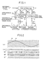
- Fig. 1 a first embodiment of a PWM controller according to the present invention.
- a plurality of PWM pattern data is stored in or read out of a PWM pattern ROM 2, and a reference voltage V* is input to the ROM 2 as a pattern selecting signal to address a PWM pattern address area of a certain voltage.
- First, second and third phase counters 4, 5 and 6 for lower, intermediate and higher bits are connected in cascade and count numbers of synchronous pulses P1 to output phase signals or counted values ⁇ L *, ⁇ M * and ⁇ H *, respectively, and by using the counted values of the synchronous pulses P1, a plurality of PWM pattern data is read out of the ROM 2 and, in the same time, the PWM pattern data having the predetermined electrical angle is addressed.
- a pulse signal having a frequency proportional to an operating frequency of an inverter to which the PWM controller of the present invention is applied is given as the synchronous pulse P1 to the first phase counter 4, as hereinafter described in detail.
- the reference voltage V* and the counted values ⁇ L *, ⁇ M * and ⁇ H * of the first, second and third phase counters 4, 5 and 6 are represented by 7 bits, 6 bits, 2 bits and 3 bits, respectively.
- the phase counter 6 is a hexadic counter to output six values ⁇ H * such as 0 to 5.
- the other counters 4 and 5 fully count within the bit numbers to output 64 values ⁇ L * such as 0 to 63 and four values ⁇ M * such as 0 to 3, respectively.
- Clock pulses having a certain frequency for use in an asynchronous PWM control hereinafter described are fed as asynchronous pulse P2 into a selector 7 along with the synchronous pulses P1, and the selector 7 selects the synchronous pulses P1 or the asynchronous pulses P2 according to a synchronous/asynchronous change signal MS as a mode signal to be fed to the selector 7 and outputs the selected pulses P1 or P2 to a modulation counter 10.
- the modulation counter 10 counts the number of the pulses P1 or P2 and sends the counted value ⁇ L *′ of 6 bits to the ROM 2.
- the bit number 6 of the counted value ⁇ L *′ of the modulation counter 10 is the same as that of the first phase counter 4.
- the mode signal MS is supplied to an AND circuit 11 where, when the mode signal MS selects the synchronous pulse P1, its gate is opened to pass a carry CRY of the the modulation counter 10 to the first phase counter 4, and the carry CRY clears the count number to naught in the first phase counter 4.
- the second phase counter 5 outputs the counted value ⁇ M * to the ROM 2.
- the ROM 2 is addressed by the code of 15 bits, i.e., the reference V*, the counted value ⁇ L *′ of the modulation counter 10 and the counted value ⁇ M * of the second phase counter 5 to output the stored PWM pattern data as signals Q out of 6 bits to a distributor 12.
- a device interchangeable with PROMi-27256 (Trade Name) of INTER CORPORATION is provided with an 8-bit data line, and its 6 bits may be used for the ROM 2.
- the 6-bit PWM data Q out is fed from the ROM 2 to a distributor 12, and the distributer 12 selects 3-bit data from the 6-bit PWM data Q out and outputs the selected 3-bit PWM pattern data as PWM control signals P out for three phases of a three-phase inverter.
- the 3-bit counted value ⁇ H * is also input from the third phase counter 6 to the distributer 12 for instructing the above data distribution operation.
- the 6-bit PWM Q out output simultaneously from the ROM 2 includes 6 data having a period of 60° and a phase difference of 60° which is obtained by dividing one period of its periodic function into six equal parts.
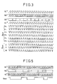
- Fig. 2a illustrates a sine wave e1 having an amplitude V* and a triangular wave e2 having a constant amplitude
- Fig. 2b shows a PWM signal obtained by comparing these two signals e1 and e2.
- the frequency of the triangular wave e2 may be determined to integral times, e.g., twice, three times or four times of 24.
- the sine wave PWM signal having the amplitude V* is obtained by setting continuity periods of positive and negative side elements of an inverter bridge to "1" and "0", respectively.
- One cycle of sine wave PWM signal shown in Fig. 2b is divided into six equal parts by the period of 60°, and thus is stored as six PWM pattern data having periods 0 - 60°, 60 - 120°, 120 - 180°, 180 - 240°, 240 - 300° and 300 - 360° in 0-bit, 1-bit, 2-bit, 3-bit, 4-bit and 5-bit of the ROM 2.
- the six PWM pattern data having the phase difference 60° from one another are simultaneously and repeatedly read out of the ROM 2 by the counted value ⁇ L *′ of the first phase counter 4 and the counted value ⁇ M * of the second phase counter 5, and the distributor 12 changes consecutively the bits every 60° period by the counted value ⁇ H * of the third phase counter 6 to output one cycle of the PWM pattern data as the PWM control signals P out .
- the PWM pattern data of Fig. 2b is obtained by continuously changing 0-bit, 1-bit, 2-bit, 3-bit, 4-bit and 5-bit of the ROM 2 using the counted value ⁇ H * of the third phase counter 6.
- the frequency of the triangular wave e2 is determined to 24 times of that of the sine wave e1
- the period of the counted value ⁇ L * of the first phase counter 4 is equal to that of the triangular wave e2.
- the first, second and third phase counters always count the synchronous pulses P1, and the relation among their counted values ⁇ L *, ⁇ M * and ⁇ H * is shown in Fig. 3.
- the synchronous/asynchronous change signal MS becomes "1"
- the selector 7 selects the synchronous pulses P1.
- the counted value ⁇ L *′ of the modulation counter 10 becomes equal to the counted value ⁇ L * of the first phase counter 4.
- the modulation counter 10 outputs the carry CRY to the AND circuit 11, and the first phase counter 4 is cleared by the carry CRY passing through the AND circuit 11. Then, the counted values of the first phase counter 4 and the modulation counter 10 are simultaneously cleared to naught by the next synchronous pulse P1, and thereafter the counted values ⁇ L * and ⁇ L *′ of the two counters 4 and 10 become equal.
- the ROM 2 outputs the 6-bit PWM pattern data e0 to e5 stored in the addresses addressed by the reference voltage V* and the counted values ⁇ M * and ⁇ L *′ of the modulation counter 10 and the second phase counter 5, as the Q out signal to the distributor 12.
- the distributor 12 changes the 3-bit PWM control signal P out so as to selectively output the PWM data, e.g., e0 ⁇ e1 ⁇ e2 ⁇ e3 ⁇ e4 ⁇ e5 ⁇ e0 for U-phase, e4 ⁇ e5 ⁇ e0 ⁇ e1 ⁇ e2 ⁇ e3 ⁇ e4 for V-phase or e2 ⁇ e3 ⁇ e4 ⁇ e5 ⁇ e0 ⁇ e1 ⁇ e2 for W-phase.
- the output data P out for the U-, V- and W-phases have the same wave form as the PWM pattern data shown in Fig. 2b, except their phase differences of 120°, and thus may be used symmetrical three phase PWM signals.
- the synchronous/asynchronous change signal MS is set to "0", and the selector 7 selects the asynchronous pulses P2.
- the counted value ⁇ L *′ of the modulation counter 10 is advanced by the asynchronous pulses P2, and the counted values ⁇ L *, ⁇ M * and ⁇ H * of the first, second and third phase counters 4, 5 and 6 are forwarded by the synchronous pulses P1.
- the synchronous/asynchronous change signal MS becomes "0" even when the modulation counter 10 outputs the carry CRY, the first phase counter 4 is not cleared. That is, in this embodiment, the modulation counter 10 is completely isolated in operation from the first, second and third phase counters, 4, 5 and 6.
- the frequency f2 of the asynchronous pulses P2 is determined to approximately 1.4 times of the frequency f1 of the synchronous pulses P1. Accordingly, in this case, one period or cycle (t0 to t1) of the counted value ⁇ L *′ of the modulation counter 10 is 1/1.4 (approximately 70%) of one cycle (t0 to t2) of the counted value ⁇ L * of the first phase counter 4.
- the phase width is compressed to approximately 70% in comparison with the one shown in Fig. 3.
- the counted value ⁇ L *′ of the modulation counter 10 is reset to "0" at the time t1, and the modulation counter 10 starts again to count the pulses.
- the counted value ⁇ M * of the second phase counter 5 is not changed in the period (t1 to t2), the pattern data is output again from the ROM 2 in the period (t0 to t1).
- the pattern data in the period (t0 to t1) is repeatedly output n times. Since f2/f1 is 1.4 in the embodiment of Fig. 4, the pattern data in the period (t1 to t2) corresponding to the former 40% of the pattern data in the period (t0 to t1) is output.
- the counted value ⁇ L * of the first phase counter 4 for counting the number of the synchronous pulses P1 overflows at a time t2 to advance the counted value ⁇ M * of the second phase counter 5 from "0" to "1" while the modulation counter 10 independently continues counting of the asynchronous pulses P2.
- the pattern data of e0 to e5 shown in Fig. 4 is read out of the ROM 2 in the same manner as described above, and the distributer 12 outputs the 3-phase PWM signals P out for the U-, V- and W-phases by the counted value ⁇ H * of the third phase counter 6 in the same manner as the synchronous PWM mode described above.
- the PWM signals each include one pulse having a different width therefrom per one cycle of the counted value ⁇ L *′ of the modulation counter 10, and act as the asynchronous PWM control signals whose pulse width modulation frequencies can be determined by the frequency f2 of the asynchronous pulses P2.
- the synchronous PWM control and the asynchronous PWM control are changed by setting the synchronous/asynchronous change signal MS to "1" or "0", and the PWM pattern data to be stored in the ROM 2 must be synchronous/asynchronous common-use pattern data including an integral number of pulses per one cycle of the counted values ⁇ M * of the second phase counter 5, as shown in Fig. 2, so as not to generate an excessive and irregular pulse having a narrow width in the asynchronous PWM control.
- various PWM pattern data may be stored at will in the ROM 2.
- the synchronous/asynchronous common-use pattern data may be used only in the asynchronous PWM control region.
- the first phase counter 4 is cleared by the next synchronous pulse P1, resulting in that the counted value ⁇ L * of the first phase counter 4 becomes equal to the counted value ⁇ L *′ of the modulation counter 10. That is, the first phase counter 4 is cleared by the synchronous pulse P1 only after the outputting of the one pulse is finished, and therefore no irregular pulse is produced when the asynchronous PWM control is changed to the synchronous PWM control. Further, at this asynchronous to synchronous change time, the voltage phase of at most one cycle of the first phase counter 4 is jumped.
- one cycle of the first phase counter 4 is determined to 15° in this embodiment, when the bit number of the first phase counter 4 and the modulation counter 10 is reduced in order to decrease one cycle, for example, to 7.5 or 3.75 while the bit number of the second phase counter 5 is enlarged, the jumped amount on changing the asynchronous PWM control to the synchronous PWM control is reduced to obtain a smooth change operation.
- the PWM pattern data of one cycle of the sine wave is entirely stored in the ROM 2 in this embodiment, by utilizing the symmetrical nature of the wave forms, only one fourth period (0 to 90°) of the PWM pattern data may be stored in the ROM 2, and the PWM pattern data may be repeatedly read out of the ROM 2 to produce one cycle of the PWM pattern data.
- the change from the synchronous PWM control to the asynchronous PWM control can be readily and smoothly carried out without any trouble because the counted values of the first phase counter 4 and the modulation counter 10 are equal at the changing moment.
- Fig. 5 shows a PWM pattern signal Q out output from the ROM 2 in the synchronous PWM control
- Fig. 6 shows another PWM pattern signal Q out having irregular pulses therein in the asynchronous PWM control with respect to the counted values ⁇ L *, ⁇ M * and ⁇ L *′ of the first and second phase counter 4 and 5 and the modulation counter 10, in which the first phase counter 4 and the modulation counter 10 are assumed to be 3 bits for the brevity of the description.
- the counted value ⁇ L *′ of the modulation counter 10 becomes equal to the counted value ⁇ L * of the first phase counter 4, and the PWM pattern data stored in the ROM 2 is read out of the ROM 2 as the output PWM pattern data Q out as it is.
- the frequency f2 of the asynchronous pulse P2 is somewhat higher than that f1 of the synchronous pulse P1
- the counted value ⁇ L *′ of the modulation counter 10 is counted somewhat faster than that ⁇ L * of the first phase counter 4.
- the output Q out of the ROM 2 changes, such as "0" at the time t4 when the counted value ⁇ L *′ of the modulation counter 10 becomes “2", “1” at the time t5 when the counted value ⁇ L *′ is “6", and "0” at the time t7 when the counted value ⁇ L *′ is "2".
- the PWM pattern data is output from the ROM 2 according to the asynchronous pulses P2 in the same manner as described above.
- the asynchronous PWM pattern data having two pulses per one cycle of the modulation counter 10 in the period (t1 to t6), as shown in Fig. 6, has an irregular pulse wave form with respect to that of Fig. 5.
- a second embodiment of a PWM controller according to the present invention which is capable of preventing the generation of the irregular pulses of the first embodiment described above.
- the PWM controller has the same construction as that of the first embodiment, except a latch circuit 13 for once latching the PWM control signals output from the distributor 12 in accordance with the pulse output from the selector 7. That is, in the asynchronous PWM control, when the output data Q out shown in Fig. 6 is output as the PWM signal from the distributor 12, the PWM pattern data which is the output data just before the counted value ⁇ L *′ of the modulation counter 10 is advanced by the asynchronous pulse P2 and is latched in the latch circuit 13, is output therefrom. Hence, the "0" periods (t2 to t3) and (t7 to t8) of the output data Q out shown in Fig. 6 can be omitted.
- a third embodiment of a PWM controller according to the present invention which is capable of preventing the production of the irregular pulses of the first embodiment.
- a chattering stopper 14 for preventing the production of the irregular pulses is additionally provided between the ROM 2 and the distributor 12, as compared with the first embodiment.
- the chattering stopper 14 removes the irregular pulses in the PWM pattern data Q out output from the ROM 2 according to the uppermost bit S of the counted value ⁇ L *′ of the modulation counter 10.
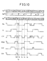
- One embodiment of the chattering stopper 14 is shown in Fig. 9.
- the chattering stopper 14 includes six pulse reforming circuits 20a to 20f for one bit and a NOT circuit 21.
- Each of the pulse reforming circuits 20 to 20f having the same construction and functions includes a NOT circuit 22, four AND circuits 23, 24, 27 and 28, an OR circuit 25 and a flip-flop circuit 26.
- the pulse reforming circuits 20a to 20f reform the PWM pattern data e0 to e5, respectively, using the uppermost bit S of the counted value ⁇ L *′ of the modulation counter 10 to output reformed data PS0 to PS5, respectively, to the distributor 12.
- the operation of one of the pulse reforming circuits 20a to 20f will be described in detail in connection with Fig. 10.
- one PWM pattern data e0 including irregular pulses, output from the ROM 2 will be reformed to the data PS0 by using the uppermost bit S of the counted value ⁇ L *′ of the modulation counter 10, as follows. That is, the two signals e0 and S are logically synthesized by the two NOT circuits 21 and 22, the two AND circuits 23 and 24 and one OR circuit 25 to obtain a signal CP, as shown in Fig. 10, which is fed as a clock signal to the flip-flop circuit 26. Logical products of the signals S and S and output signals Q and Q ( PS0 and PS0) of the flip-flop circuit 26 are input as signals DJ and DK to input terminals J and K of the flip-flop circuit 26 through the AND circuits 27 and 28.
- the flip-flop circuit 26 is in the restrained state and is not changed by the clock signal CP. Even when the clock signal CP is changed to "0" or “1” at the time t2 or t3, the output signal PS0 is not changed to be “0”. Then, when the signal S becomes "1" at the time t4, the input signal DJ of the flip-flop circuit 26 is changed to "1", and the output signal PS0 of the flip-flop circuit 26 may be changed to "1” by the clock signal CP. Hence, when the clock signal CP is changed from “0" to "1” at the time t5, the output signal PS0 of the flip-flop circuit 26 is changed from "0" to "1".
- the irregular pulses included in the signal e0 output from the ROM 2 is removed in the pulse reforming circuit 20a, and the signal PS0 including only one pulse per one cycle of the modulation counter 10 is output from the pulse reforming circuit 20a, and the modulation frequency becomes constant. Further, the duty factor of the output signal PS0 of the pulse reforming circuit 20a becomes an intermediate value between those of the output signals of the ROM 2 when the counted values ⁇ M * of the second phase counter 5 are n and n+1.
- the output signal PS0 is allowed once to change from “1” to “0” in the former half of one cycle of the modulation counter 10, and is also allowed once to change from “0" to "1” in the latter half of the one cycle of the modulation counter 10, thereby removing the irregular pulses, because of the PWM pattern data stored in the ROM 2 changes "1" ⁇ 0 ⁇ "1" in one cycle of the synchronous control, as shown in Fig. 2b.
- the output signal PS0 may be allowed once to change from “0" to "1” in the former half of one cycle of the modulation counter 10 and also be allowed once change from “1” to "0” in the latter half of the one cycle of the modulation counter 10 in the pulse reforming circuits 20a to 20f.
- the limited conditions of the PWM pattern data in the second embodiment shown in Fig. 6 are unnecessary, and, even when the difference between the leading and training addresses of th PWM pattern data in the adjacent two counted values ⁇ M * of the second phase counter 5 is more than one, the irregular pulses may be removed as described above. Accordingly, in addition to the three-phase sine wave PWM pattern data, the present invention may be applied to two-phase sine wave PWM pattern data (one phase is fixed to a certain positive or negative voltage and only the other two phases are controlled to control the voltages among the three phases to approximate sine waves).
- chattering stopper 14 is positioned between the ROM 2 and the distributor 12 in the third embodiment, the chattering stopper 14 may be placed in the output side of the distributor 12 to output the PWM control pattern data, and, in this case, it requires only three pulse reforming circuits, which is economical and simple in construction.
- the first phase counter 4 is cleared by the carry CRY of the modulation counter 10 in the synchronous PWM control in order to prevent the overcurrent since a pulse having a wider width than that in the normal operation when the synchronous PWM control is changed to the asynchronous PWM control.
- the modulation counter 10 may be cleared by the carry CRY of the first phase counter 4 in the synchronous PWM control.
- the pulse having a wide width is produced, but its influence is very small.
- there is no phase jump when the change between the synchronous and asynchronous PWM controls is carried out.
- both in the synchronous PWM pattern data and the synchronous/asynchronous common use PWM pattern data may be stored in the ROM 2, and one of them may be selected by the synchronous/asynchronous change signal MS.
- the modulation frequency of the PWM pattern data varies depending on the output frequency of the inverter.
- the modulation frequency does not vary in the asynchronous PWM control, and it may be advantageous to select the asynchronous PWM control in a certain voltage depending on noisy or other operational conditions. In these cases, the synchronous/asynchronous changes can be carried out regardless of the reference voltage V * .
- the PWM pattern data read out of the memory becomes the pattern addressed by the intermediate and lower bits (electrical angles ⁇ M * + ⁇ L *) of the first and second phase counters, and this pattern data is distributed by the higher bit value ⁇ H * of the third phase counter, thereby operating in the synchronous PWM control which is capable of outputting the optimum pattern data stored in the memory.
- the frequency of the counted value ⁇ L *′ of the modulation counter becomes different from that of the lower bit value ⁇ L * of the first phase counter.
- the modulation counter is repeatedly counted in some cycles to repeatedly output the same value ⁇ L *′ during the time of the constant value ⁇ M * to be fed to the memory.
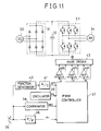
- a three-phase commercial power source 30 is connected to a rectifier 31 for rectifying an alternating voltage into a direct voltage, and a capacitor 32 is coupled to the rectifier 31 in parallel therewith.
- An inverter 33 for converting a direct voltage into an alternating voltage is connected to the rectifier 31 and the capacitor 32 in parallel therewith, and a three-phase induction motor 34 is connected to the inverter 33.
- a frequency settler 35 for setting up the fundamental frequency of the alternating voltage output by the inverter 33 is connected to a voltage-frequency (V/F) converter 36, a comparator 38 and a function generator 40.
- the V/F converter 36 outputs the synchronous pulses P1 in proportion to the output voltage of the frequency settler 35 to the PWM controller 37 according to the present invention.
- the comparator 38 When the output voltage of the frequency settler 35 is more than or at most a predetermined voltage, the comparator 38 outputs a logical value "1" or "0" as the synchronous/asynchronous change signal MS to the PWM controller 37, and an oscillator 39 generates a clock pulse having a certain frequency as the asynchronous pulse P2 to the PWM controller 37.
- the function generator 40 outputs the reference voltage V * to the PWM controller 37 through an analog-digital (A/D) converter 41.
- the PWM controller 37 outputs the three-phase PWM control signals P out for the U-, V- and W-phases to a base driver 43 directly or via three NOT circuits 42a, 42b and 42c for the U-, V- and W-phases.
- the three-phase PWM control signals P out are amplified in the base driver 43, and the amplified PWM control signals are fed to the inverter 33 for driving the corresponding switching elements therein.
- the PWM pattern data such as a synchronous/asynchronous common use pattern data for use in a low voltage region and a synchronous exclusive use pattern data of a low-dimensional harmonic elimination PWM control system for use in a high voltage region is stored in the ROM 2 within the PWM controller 37.
- the change signal MS selects the asynchronous pulses P2
- the PWM controller 37 reads out the synchronous/asynchronous common use pattern data according to the asynchronous pulses P2 output by the oscillator 39 to operate the inverter 33 in the asynchronous PWM control where the modulation frequency is constant.
- the change signal MS selects the synchronous pulses P1
- PWM controller 37 reads out the synchronous/asynchronous common use pattern data according to the synchronous pulses P1 output by the V/F converter 36 to operate the inverter 33 in the synchronous PWM control, in which the modulation frequency is proportional to the operating frequency.
- the ROM 2 outputs the synchronous pattern data of the low-dimensional harmonic elimination PWM control system to operate the inverter 33 in the synchronous PWM control of the low-dimensional harmonic elimination PWM control system.
- the inverter may be operated in the asynchronous PWM control corresponding to the triangular wave comparison in the low speed region, in the synchronous PWM control corresponding to the triangular wave comparison in the intermediate speed region or in the synchronous PWM control of the low-dimensional harmonic elimination control system in the high speed region.
- the inverter 33 can be operated in the optimum PWM control system depending on the frequency from the low speed region to the high speed region, and the low current ripple and the high efficient PWM control can be performed in the wide operational frequency range.
- asynchronous PWM control by a PWM controller including a memory in which PWM pattern data is stored. Since a synchronous/asynchronous common use pattern data is prepared for the PWM pattern data corresponding to a triangular wave comparison, it is possible to conduct three PWM controls such as the asynchronous PWM control corresponding to the triangular wave comparison, the synchronous PWM control corresponding to the triangular wave comparison and the PWM control using the pattern data calculated in various conventional off-lines. Further, it is possible to carry out various PWM controls depending on the operational frequency and the output voltage, and the extension of the operational frequency range and the highly effective operation can be performed. Furthermore, the asynchronous PWM control can be conducted using the memory without providing a particular asynchronous PWM controller, the economical and widely used PWM controller can be provided.
Landscapes
- Engineering & Computer Science (AREA)
- Power Engineering (AREA)
- Inverter Devices (AREA)
Claims (8)
- Eine PWM Steuereinrichtung (37) für einen Energiewandler, umfassend:
Ein Phasenzähler-Mittel (4,5,6), um synchrone Pulse zu zählen;
Ein Speicher-Mittel (2);
Ein Verteiler-Mittel (12), das obere Bit des Phasensignals verwendend;
Ein Modulations-Mittel (10), um einen Wert an das Speicher-Mittel (2) auszugeben, wobei der Wert des Modulations-Mittels (10) anstatt des niedrigeren Bits des Phasensignals verwendet wird, dadurch gekennzeichnet, daß
besagte synchrone Pulse eine proportionale Frequenz zu der eines Inverters (33) haben, der gesteuert werden soll, um ein Phasensignal auszugeben;
besagtes Speicher-Mittel (2) mindestens zwei PWM Muster-Daten mit Adressen speichert, wobei die PWM Muster-Daten ausgelesen werden durch Adressierung unter Verwendung eines Muster-Wahlsignals und des Phasensignals;
besagtes Verteiler-Mittel (12) die aus dem Speicher-Mittel (2) ausgelesenen PWM Muster-Daten verteilt; das obere Bit verwendend, um PWM Siganle auszugeben, um den Inverter (33) zu steuern; und
besagtes Modulations-Mittel (10) ein Modulationszähler-Mittel (10) ist, um einen der synchronen Pulse und asynchronen Pulse mit einer bestimmten Frequenz zu zählen, wobei der eine der synchronen und asynchronen Pulse gemäß eines Modus-Signals ausgewält wird, wobei der von dem Modulations-Mittel (10) gezählte Wert verwendet wird, um selektiv die PWM Signale einer der synchronen und asynchronen Steuerungen auszugeben. - Die Steuereinrichtung (37) von Patentanspruch 1, worin die PWM Muster-Daten einen Puls in einem Zyklus des niedrigeren Bits des Phasenzähler-Mittels (4,5,6) einschließen und das PWM Signal mindestens einen Puls in einem Zyklus des niedrigeren Bits des Phasenzähler-Mittels (4,5,6) einschließt.
- Die Steuereinrichtung (37) von Patentanspruch 1, worin, wenn das Modus-Signal die synchronen Pulse auswählt, eine Übertrag-Signalausgabe von einem der Modulationszähler (10) und der Phasenzähler (4,5,6) die Zählwerte der anderen Modulationszähler (10) und Phasenzähler (4,5,6) löschen.
- Die Steuereinrichtung (37) von Patentanspruch 1, worin das Phasenzähler-Mittel (4,5,6) einen ersten (4), zweiten (5) und dritten (6) Phasenzähler enthält, um die niedrigeren, zwischenliegenden und höheren Bits des Phasensignals zu zählen.
- Die Steuereinrichtung (37) von Patentanspruch 1, worin einer der synchronen und asynchronen Pulse gemäß dem Modus-Signal in einer Wähleinrichtung (7) ausgewählt wird.
- Die Steuereinrichtung (37) von Patentanspruch 1, worin ein AND Schaltkreis selektiv das Übertrag-Signal weiterleitet.
- Die Steuereinrichtung (37) von Patentanspruch 1, ebenso beinhaltend ein Verriegelungs-Mittel (13), um eines der aus dem Speicher-Mittel (2) ausgelesenen PWM Muster-Daten, und der vom Verteiler-Mittel (12) ausgegebenen PWM Signale bei jedem Puls, der an den Modulationszähler (10) zugeführt werden soll, zu verriegeln, um eine Erzeugung von mindestens einem irregulären Puls in der asynchronen PWM Steuerung zu verhindern.
- Die Steuereinrichtung (37) von Patentanspruch 1, ebenfalls beinhaltend ein Prell-Unterdrückungsglied-Mittel (14) für einmaliges Verriegeln einer der aus dem Speicher-Mittel (2) ausgelesenen führenden und nachgezogenen PWM Muster-Daten und der von dem Verteiler-Mittel in einem ersten oder zweiten Halbzyklus des Modulations-Mittels (10) ausgegebenen PWM Signale, um eine Erzeugung von mindestens einem irregulärem Puls in der asynchronen PWM Steuerung zu verhindern.
Applications Claiming Priority (2)
| Application Number | Priority Date | Filing Date | Title |
|---|---|---|---|
| JP62284217A JPH0681513B2 (ja) | 1987-11-12 | 1987-11-12 | Pwm制御装置 |
| JP284217/87 | 1987-11-12 |
Publications (3)
| Publication Number | Publication Date |
|---|---|
| EP0316006A2 EP0316006A2 (de) | 1989-05-17 |
| EP0316006A3 EP0316006A3 (en) | 1989-12-06 |
| EP0316006B1 true EP0316006B1 (de) | 1993-05-19 |
Family
ID=17675683
Family Applications (1)
| Application Number | Title | Priority Date | Filing Date |
|---|---|---|---|
| EP88118835A Expired - Lifetime EP0316006B1 (de) | 1987-11-12 | 1988-11-11 | Pulsbreitenmodulierte Steuereinrichtung |
Country Status (6)
| Country | Link |
|---|---|
| US (1) | US4860186A (de) |
| EP (1) | EP0316006B1 (de) |
| JP (1) | JPH0681513B2 (de) |
| KR (1) | KR920004905B1 (de) |
| CN (1) | CN1010362B (de) |
| DE (1) | DE3881161T2 (de) |
Families Citing this family (23)
| Publication number | Priority date | Publication date | Assignee | Title |
|---|---|---|---|---|
| EP0760578B1 (de) * | 1989-10-02 | 2003-04-02 | Canon Kabushiki Kaisha | Bilderzeugungsgerät und Modulationsverfahren |
| AT401450B (de) * | 1989-10-09 | 1996-09-25 | Fronius Schweissmasch | Steuerverfahren für dreiphasige bidirektionale pulsumrichter hoher taktzahl |
| US5418932A (en) * | 1990-02-01 | 1995-05-23 | Hitachi, Ltd. | Generation of width modulated pulses by relatively adjusting rising and falling edges upon comparison of counter with programmably stored values |
| US4994950A (en) * | 1990-07-31 | 1991-02-19 | Eaton Corporation | Waveform generator for inverter control |
| US5506487A (en) * | 1991-03-28 | 1996-04-09 | General Electric Company | Systems and methods for driving a compressor with a motor |
| US5400237A (en) * | 1992-05-11 | 1995-03-21 | Simmonds Precision Products, Inc. | PWM inverter controller with waveform memory |
| US5615099A (en) * | 1994-08-24 | 1997-03-25 | Kabushiki Kaisha Toshiba | Control system for single-phase PWM converter |
| DE19541832A1 (de) * | 1995-11-10 | 1997-05-15 | Thomson Brandt Gmbh | Motorsteuerung für elektronisch kommutierende Gleichstrommotoren zur Kompensation von Drehmomenteinbrüchen |
| US5835363A (en) * | 1997-11-13 | 1998-11-10 | Acer Peripherals, Inc. | Power supply device featuring synchronous mode and asynchronous mode operation |
| US7049771B2 (en) * | 2004-01-27 | 2006-05-23 | Nippon Yusoki Co., Ltd. | Multi-phase carrier signal generator and multi-phase carrier signal generation method |
| US7049778B2 (en) * | 2004-02-09 | 2006-05-23 | Nippon Yusoki Co., Ltd. | Inverter control apparatus and inverter control method |
| FI118875B (fi) * | 2006-09-26 | 2008-04-15 | Vacon Oyj | Invertterien rinnankytkentä |
| WO2009040884A1 (ja) * | 2007-09-25 | 2009-04-02 | Mitsubishi Electric Corporation | 電動機の制御装置 |
| JP5253828B2 (ja) * | 2008-01-25 | 2013-07-31 | ルネサスエレクトロニクス株式会社 | モータ駆動装置および半導体集積回路装置 |
| US8890457B2 (en) * | 2008-09-19 | 2014-11-18 | Hewlett-Packard Development Company, L.P. | Systems and methods for controlling motors |
| JP4858597B2 (ja) | 2008-11-28 | 2012-01-18 | 株式会社デンソー | 回転機の制御装置及びその製造方法 |
| US8345451B2 (en) * | 2009-11-08 | 2013-01-01 | Wernlund James V | DC to AC converter that generates the sine wave from the pulse width modulated signal |
| DE102010003527A1 (de) * | 2010-03-31 | 2011-10-06 | Robert Bosch Gmbh | Verfahren zum Ansteuern eines Elektromotors |
| US9768755B2 (en) * | 2013-04-09 | 2017-09-19 | Hamilton Sundstrand Corporation | Lookup table assisted pulse width modulation |
| AT515243A1 (de) * | 2013-12-19 | 2015-07-15 | Schneider Electric Power Drives Gmbh | Verfahren zur Ansteuerung parallel geschalteter Inverter |
| JP7096679B2 (ja) * | 2018-03-16 | 2022-07-06 | 日立Astemo株式会社 | モータ制御装置 |
| TWI775482B (zh) * | 2021-06-10 | 2022-08-21 | 茂達電子股份有限公司 | 馬達驅動控制系統 |
| CN119318090A (zh) * | 2022-03-24 | 2025-01-14 | 阿尔法能源技术公司 | 用于能量存储系统的通信系统和同步技术 |
Family Cites Families (9)
| Publication number | Priority date | Publication date | Assignee | Title |
|---|---|---|---|---|
| US4099109A (en) * | 1976-10-01 | 1978-07-04 | Westinghouse Electric Corp. | Digital apparatus for synthesizing pulse width modulated waveforms and digital pulse width modulated control system |
| JPS573582A (en) * | 1980-06-05 | 1982-01-09 | Toshiba Corp | Controller for inverter |
| JPS6014693A (ja) * | 1983-07-05 | 1985-01-25 | 松下電工株式会社 | 波付可撓管用継手 |
| JPH07108095B2 (ja) * | 1984-01-20 | 1995-11-15 | 株式会社日立製作所 | インバータ装置及びその制御方法 |
| JPH065989B2 (ja) * | 1984-01-23 | 1994-01-19 | 富士電機株式会社 | インバ−タのpwm信号発生装置 |
| JPS60174088A (ja) * | 1984-02-17 | 1985-09-07 | Fanuc Ltd | 交流電動機のデジタル制御方式 |
| JPS62118774A (ja) * | 1985-11-18 | 1987-05-30 | Toshiba Corp | インバ−タのパルス幅変調信号発生方式 |
| JPH07112360B2 (ja) * | 1986-07-25 | 1995-11-29 | 株式会社日立製作所 | Pwmインバ−タの制御方法および装置 |
| JPH0779551B2 (ja) * | 1987-03-20 | 1995-08-23 | 株式会社日立製作所 | インバ−タ制御装置 |
-
1987
- 1987-11-12 JP JP62284217A patent/JPH0681513B2/ja not_active Expired - Lifetime
-
1988
- 1988-11-08 US US07/268,567 patent/US4860186A/en not_active Expired - Fee Related
- 1988-11-11 EP EP88118835A patent/EP0316006B1/de not_active Expired - Lifetime
- 1988-11-11 DE DE88118835T patent/DE3881161T2/de not_active Expired - Fee Related
- 1988-11-12 KR KR1019880014880A patent/KR920004905B1/ko not_active Expired
- 1988-11-12 CN CN88107833A patent/CN1010362B/zh not_active Expired
Also Published As
| Publication number | Publication date |
|---|---|
| JPH0681513B2 (ja) | 1994-10-12 |
| DE3881161D1 (de) | 1993-06-24 |
| EP0316006A3 (en) | 1989-12-06 |
| US4860186A (en) | 1989-08-22 |
| KR920004905B1 (ko) | 1992-06-22 |
| CN1010362B (zh) | 1990-11-07 |
| CN1033134A (zh) | 1989-05-24 |
| KR890009064A (ko) | 1989-07-15 |
| DE3881161T2 (de) | 1993-10-21 |
| JPH01129774A (ja) | 1989-05-23 |
| EP0316006A2 (de) | 1989-05-17 |
Similar Documents
| Publication | Publication Date | Title |
|---|---|---|
| EP0316006B1 (de) | Pulsbreitenmodulierte Steuereinrichtung | |
| EP0593738B1 (de) | Programmierter pbm-umrichterregler | |
| EP0086650B1 (de) | Gerät zur Erzeugung einer gesteuerten, leistungsbehafteten Wellenform | |
| US4599685A (en) | Control circuit for power converter apparatus | |
| EP1172926B1 (de) | Stromversorgungsvorrichtung | |
| EP0371442A1 (de) | Steuerverfahren für Wechselrichter mit Pulsbreitenmodulation und Wechselrichtersystem mit Pulsbreitenmodulation | |
| EP0077836B1 (de) | Steuerung für elektromotoren | |
| US4352154A (en) | Varying two phase voltages in dc to three phase converter | |
| EP0467694B1 (de) | Vorrichtung zur Erzeugung eines dreiphasigen PWM-Signals für Wechselrichter | |
| US4924168A (en) | Control apparatus for PWM-controlled, variable voltage/variable frequency inverters | |
| US20080291698A1 (en) | Control Method and Controller for Pwm Cyclo-Converter | |
| JPH09182452A (ja) | 3レベルインバータ装置 | |
| GB2125239A (en) | A three phase supply synthesis arrangement | |
| GB2171266A (en) | PWM inverter | |
| US4688163A (en) | Method for controlling the phase angle of the output current or the output voltage of a frequency converter and apparatus for carrying out the method | |
| JPH0447553B2 (de) | ||
| JPS6159062B2 (de) | ||
| KR940007971B1 (ko) | 룸에어콘의 인버터 제어 방법 | |
| JPH06178593A (ja) | 電動機の可変速駆動装置 | |
| JPH0767287B2 (ja) | インバータ制御装置 | |
| JPS61177174A (ja) | インバ−タの制御装置 | |
| JPS6285678A (ja) | インバ−タ制御回路 | |
| JPH0348753B2 (de) | ||
| JPS59127577A (ja) | 電圧形pwmインバ−タの制御方法 | |
| JPH08214555A (ja) | 3相電圧形インバータのためのpwm方法及び装置 |
Legal Events
| Date | Code | Title | Description |
|---|---|---|---|
| PUAI | Public reference made under article 153(3) epc to a published international application that has entered the european phase |
Free format text: ORIGINAL CODE: 0009012 |
|
| 17P | Request for examination filed |
Effective date: 19881111 |
|
| AK | Designated contracting states |
Kind code of ref document: A2 Designated state(s): DE FR GB |
|
| PUAL | Search report despatched |
Free format text: ORIGINAL CODE: 0009013 |
|
| AK | Designated contracting states |
Kind code of ref document: A3 Designated state(s): DE FR GB |
|
| RHK1 | Main classification (correction) |
Ipc: H02M 7/5387 |
|
| 17Q | First examination report despatched |
Effective date: 19920115 |
|
| GRAA | (expected) grant |
Free format text: ORIGINAL CODE: 0009210 |
|
| AK | Designated contracting states |
Kind code of ref document: B1 Designated state(s): DE FR GB |
|
| REF | Corresponds to: |
Ref document number: 3881161 Country of ref document: DE Date of ref document: 19930624 |
|
| ET | Fr: translation filed | ||
| PLBE | No opposition filed within time limit |
Free format text: ORIGINAL CODE: 0009261 |
|
| STAA | Information on the status of an ep patent application or granted ep patent |
Free format text: STATUS: NO OPPOSITION FILED WITHIN TIME LIMIT |
|
| 26N | No opposition filed | ||
| PGFP | Annual fee paid to national office [announced via postgrant information from national office to epo] |
Ref country code: GB Payment date: 19941101 Year of fee payment: 7 |
|
| PGFP | Annual fee paid to national office [announced via postgrant information from national office to epo] |
Ref country code: FR Payment date: 19951109 Year of fee payment: 8 |
|
| PG25 | Lapsed in a contracting state [announced via postgrant information from national office to epo] |
Ref country code: GB Effective date: 19951111 |
|
| PGFP | Annual fee paid to national office [announced via postgrant information from national office to epo] |
Ref country code: DE Payment date: 19951113 Year of fee payment: 8 |
|
| GBPC | Gb: european patent ceased through non-payment of renewal fee |
Effective date: 19951111 |
|
| PG25 | Lapsed in a contracting state [announced via postgrant information from national office to epo] |
Ref country code: FR Effective date: 19970731 |
|
| PG25 | Lapsed in a contracting state [announced via postgrant information from national office to epo] |
Ref country code: DE Effective date: 19970801 |
|
| REG | Reference to a national code |
Ref country code: FR Ref legal event code: ST |