EP0314366A2 - Strahlungsabsorber und Verfahren zu seiner Herstellung - Google Patents
Strahlungsabsorber und Verfahren zu seiner Herstellung Download PDFInfo
- Publication number
- EP0314366A2 EP0314366A2 EP88309752A EP88309752A EP0314366A2 EP 0314366 A2 EP0314366 A2 EP 0314366A2 EP 88309752 A EP88309752 A EP 88309752A EP 88309752 A EP88309752 A EP 88309752A EP 0314366 A2 EP0314366 A2 EP 0314366A2
- Authority
- EP
- European Patent Office
- Prior art keywords
- radiation
- absorber
- mould
- electrically insulating
- inert
- Prior art date
- Legal status (The legal status is an assumption and is not a legal conclusion. Google has not performed a legal analysis and makes no representation as to the accuracy of the status listed.)
- Withdrawn
Links
Images
Classifications
-
- H—ELECTRICITY
- H01—ELECTRIC ELEMENTS
- H01Q—ANTENNAS, i.e. RADIO AERIALS
- H01Q17/00—Devices for absorbing waves radiated from an antenna; Combinations of such devices with active antenna elements or systems
- H01Q17/008—Devices for absorbing waves radiated from an antenna; Combinations of such devices with active antenna elements or systems with a particular shape
-
- H—ELECTRICITY
- H01—ELECTRIC ELEMENTS
- H01Q—ANTENNAS, i.e. RADIO AERIALS
- H01Q17/00—Devices for absorbing waves radiated from an antenna; Combinations of such devices with active antenna elements or systems
- H01Q17/004—Devices for absorbing waves radiated from an antenna; Combinations of such devices with active antenna elements or systems using non-directional dissipative particles, e.g. ferrite powders
Definitions
- This invention relates to radiation absorbers and in particular to radiation absorbers suitable for use with radiation having a frequency of the order of 1THz (1012Hz, 0.3mm wavelength).
- Radiation absorbers are used for mode control in microwave cavities and tubes and in waveguides. They are also used for protecting radio equipment from interference and vehicles from detection.
- the conventional microwave absorbers increase in reflectivity as the radiation frequency is increased.
- One known method of reducing the reflectivity of an absorbent material is to profile the irradiated surface (e.g. to form an array of pyramids) thus producing multiple reflections and enhancing the absorption of the incident radiation.
- the conventional microwave absorbers are not, in general, suitable for absorbing radiation having a frequency above 300 GHz (wavelength less than 1mm).
- One object of the present invention is to provide a radiation absorber having a high reflection loss when irradiated at a frequency in the range 0.5 - 2.5THz.
- Another object of the present invention is to provide a radiation absorbent material suitable for absorbing irradiation in the frequency range 0.5 - 2.5 THz, the material having a sufficiently low viscosity to facilitate moulding to provide the required profile.
- a radiation absorber for absorbing radiation in the frequency range 0.5 - 2.5THz comprising: a body of cured, electrically insulating, silcone-based elastomer containing an inert, electrically insulating, powdered siliceous filler, the surface exposed to the radiation being profiled to enhance the absorption of said radiation by said absorber and to reduce the reflectivity in the said frequency range.
- the silicone-based elastomer with an inert siliceous filler comprises "Silcoset 100", which is cured by mixing with "Curing Agent A”, both materials being manufactured by Imperial Chemical Industries, p.l.c.
- the profiled surface of the elastomer conveniently comprises either two or three mutually inclined sets of parallel V-grooves arranged to provide an array of sharp-pointed pyramids having bases shaped as either parallelograms (preferably square) or triangles (preferably equilateral). It is desirable that flat regions between the pyramids and at their apeces should be completely eliminated.
- a mould suitable for manufacturing a sheet of profiled radiation absorbent material comprises a mould with an appropriately profiled base, the mould being made of cured silicone based elastomer filled with an inert siliceous filler, and the inner surface of the mould being treated to prevent damage to the profiled sheet during the extraction from the mould.
- a silicone-based elastomer containing an inert siliceous filler after curing, provides an excellent absorber of radiation in the frequency range 0.5 - 2.5THz, and that this material has a sufficiently low viscosity before curing to enable it to be moulded to give the required profile.
- a flat surface of cured Silcoset 100 has a reflection loss of 15dB for a radiation frequency of 1.0THz, which compares favourably with the 11dB reflection loss of the best material, described by Hemmati et al and discussed hereinbefore.
- a preferred profile geometry for high reflection loss at a frequency between 0.5 and 2.5THz comprises an array of square based pyramids of height beteen 1.0 and 3.0mm with the four triangular faces each inclined at 25° - 30° to the pyramid axis. At a frequency of 1.5THz the pyramids are preferably 2.0mm high with the triangular faces each inclined at 25° to the pyramid axis. Measurements on cured Silcoset 100 with this profile are given in the table.
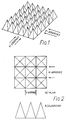
- Figure 1 shows a general view and Figures 2(a) and 2(b) plan and elevation views of an array of square based pyramids formed by two orthogonal sets of parallel V-grooves, which are indicated by the arrows.
- a readily machined material such as perspex is profiled to the shape shown in Figure 1 by machining two perpendicular sets of parallel V-grooves arranged to provide sharp pointed pyramids 2.0mm high with the side faces of the pyramids inclined at 25° to the pyramid axis.
- This model is used for forming a mould of Silcoset 100 cured with Curing Agent A.
- the inside of the mould is coated with a metal layer such as vacuum evaporated aluminium to prevent sticking and damage.
- Sheets of the profiled radiation absorbent material can be repeatedly produced by pouring Silcoset 100 mixed with the Curing Agent A into the mould, allowing the Silcoset 100 to be cured and then removing it from the mould.
- two parallel sets of V-grooves can be arranged to provide pyramids having bases in the shape of any parallelogram.
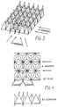
- three sets of parallel V-grooves are used to form sharp-pointed triangular based pyramids. Plan and elevation views of this arrangement are shown in Figures 4(a) and 4(b) respectively.
- An example of the arrangement in Figure 3 is illustrated by considering the four pyramids PABD, QDEB, RBCE and SDEF, as shown also in Figures 4(a) and 4(b).
- the apeces are P, Q, R, S and the triangular bases are ABD, DBE, BCE, DEF respectively.
- the pyramid QDBE has common edges BD with pyramid PABD, BE with pyramid RBCE and DE with pyramid SDEF.
- the pyramids should preferably be 2.0mm high and the pyramid side faces should be inclined at 25° to the pyramid axis.
- a radiation absorber according to the invention is highly effective for radiation of frequencies between 0.5 and 2.5THz. It is easily manufactured from readily available materials by cold setting in a mould. It is easily cut to any required shape and is sufficiently flexible to be attached to non-flat surfaces.
Landscapes
- Shielding Devices Or Components To Electric Or Magnetic Fields (AREA)
- Aerials With Secondary Devices (AREA)
- Compositions Of Macromolecular Compounds (AREA)
- Inorganic Insulating Materials (AREA)
Applications Claiming Priority (2)
| Application Number | Priority Date | Filing Date | Title |
|---|---|---|---|
| GB878725110A GB8725110D0 (en) | 1987-10-27 | 1987-10-27 | Radiation absorber & method of making it |
| GB8725110 | 1987-10-27 |
Publications (2)
| Publication Number | Publication Date |
|---|---|
| EP0314366A2 true EP0314366A2 (de) | 1989-05-03 |
| EP0314366A3 EP0314366A3 (de) | 1990-03-28 |
Family
ID=10625941
Family Applications (1)
| Application Number | Title | Priority Date | Filing Date |
|---|---|---|---|
| EP88309752A Withdrawn EP0314366A3 (de) | 1987-10-27 | 1988-10-18 | Strahlungsabsorber und Verfahren zu seiner Herstellung |
Country Status (3)
| Country | Link |
|---|---|
| US (1) | US4942402A (de) |
| EP (1) | EP0314366A3 (de) |
| GB (1) | GB8725110D0 (de) |
Cited By (3)
| Publication number | Priority date | Publication date | Assignee | Title |
|---|---|---|---|---|
| EP0402970A1 (de) * | 1989-06-15 | 1990-12-19 | Siemens Telecomunicazioni S.P.A. | Verfahren zur Ausbildung von Absorbern für elektromagnetische Felder |
| DE102006011964A1 (de) * | 2006-03-15 | 2007-09-20 | Fraunhofer-Gesellschaft zur Förderung der angewandten Forschung e.V. | Verfahren zur Bearbeitung eines optischen Elements, zur Herstellung eines Prägewerkzeugs, Verwendung einer Bearbeitungsmaschine sowie optisches Element zur Verwendung im Terahertz-Wellengebiet |
| RU2589501C1 (ru) * | 2014-12-29 | 2016-07-10 | Российская Федерация, От Имени Которой Выступает Министерство Промышленности И Торговли Российской Федерации | Устройство с пониженным коэффициентом отражения радиоволн в широком диапазоне частот |
Families Citing this family (9)
| Publication number | Priority date | Publication date | Assignee | Title |
|---|---|---|---|---|
| US5208599A (en) * | 1991-08-28 | 1993-05-04 | Ohio State University | Serrated electromagnetic absorber |
| US5260513A (en) * | 1992-05-06 | 1993-11-09 | University Of Massachusetts Lowell | Method for absorbing radiation |
| US5844518A (en) * | 1997-02-13 | 1998-12-01 | Mcdonnell Douglas Helicopter Corp. | Thermoplastic syntactic foam waffle absorber |
| JP2003229691A (ja) * | 2002-01-31 | 2003-08-15 | Riken Corp | 電波吸収体 |
| US7250920B1 (en) | 2004-09-29 | 2007-07-31 | The United States Of America As Represented By The Secrtary Of The Navy | Multi-purpose electromagnetic radiation interface system and method |
| US20060243667A1 (en) * | 2005-05-02 | 2006-11-02 | Andrew Stone | Filtrate composition with a radiation absorber |
| EP1955084A1 (de) * | 2005-11-30 | 2008-08-13 | Astrium GmbH | Hochfrequenzmesshalle zur vermessung von grossen messobjekten |
| CN104774472A (zh) * | 2015-04-10 | 2015-07-15 | 大连东信微波技术有限公司 | 一种超宽频带太赫兹吸波材料 |
| US9691509B1 (en) | 2016-07-27 | 2017-06-27 | Archit Lens Technology Inc. | Terahertz-gigahertz system housing capable of minimizing interference and noise |
Family Cites Families (16)
| Publication number | Priority date | Publication date | Assignee | Title |
|---|---|---|---|---|
| US2923689A (en) * | 1953-08-31 | 1960-02-02 | Alvin R Saltzman | Electromagnetic wave energy absorbing material |
| US3836967A (en) * | 1958-03-10 | 1974-09-17 | R Wright | Broadband microwave energy absorptive structure |
| US4023174A (en) * | 1958-03-10 | 1977-05-10 | The United States Of America As Represented By The Secretary Of The Navy | Magnetic ceramic absorber |
| GB829614A (en) * | 1958-07-08 | 1960-03-02 | Edward Bellamy Mcmillan | Microwave-radiation absorbers |
| US3887920A (en) * | 1961-03-16 | 1975-06-03 | Us Navy | Thin, lightweight electromagnetic wave absorber |
| US4024318A (en) * | 1966-02-17 | 1977-05-17 | Exxon Research And Engineering Company | Metal-filled plastic material |
| US3680107A (en) * | 1967-04-11 | 1972-07-25 | Hans H Meinke | Wide band interference absorber and technique for electromagnetic radiation |
| US4173018A (en) * | 1967-07-27 | 1979-10-30 | Whittaker Corporation | Anti-radar means and techniques |
| US4006479A (en) * | 1969-02-04 | 1977-02-01 | The United States Of America As Represented By The Secretary Of The Air Force | Method for dispersing metallic particles in a dielectric binder |
| DE1955834C3 (de) * | 1969-11-06 | 1974-01-24 | Vorwerk & Sohn, 5600 Wuppertalbarmen | Erhöhung der Absorption elektromagnetischer Wellen bei der Wärmebehandlung gefüllter oder ungefüllter Massen |
| DE2156939A1 (de) * | 1971-11-16 | 1973-05-24 | Spinner Gmbh Elektrotech | Masseabsorber fuer hochfrequenz |
| US3894169A (en) * | 1972-02-18 | 1975-07-08 | Rockwell International Corp | Acoustical damping structure and method of preparation |
| US4164718A (en) * | 1976-07-09 | 1979-08-14 | California Institute Of Technology | Electromagnetic power absorber |
| US4353069A (en) * | 1980-09-10 | 1982-10-05 | Handel Peter H | Absorptive coating for the reduction of the reflective cross section of metallic surfaces and control capabilities therefor |
| US4496950A (en) * | 1982-07-16 | 1985-01-29 | Hemming Leland H | Enhanced wide angle performance microwave absorber |
| US4539433A (en) * | 1982-11-24 | 1985-09-03 | Tdk Corporation | Electromagnetic shield |
-
1987
- 1987-10-27 GB GB878725110A patent/GB8725110D0/en active Pending
-
1988
- 1988-10-18 EP EP88309752A patent/EP0314366A3/de not_active Withdrawn
- 1988-10-26 US US07/262,798 patent/US4942402A/en not_active Expired - Fee Related
Cited By (3)
| Publication number | Priority date | Publication date | Assignee | Title |
|---|---|---|---|---|
| EP0402970A1 (de) * | 1989-06-15 | 1990-12-19 | Siemens Telecomunicazioni S.P.A. | Verfahren zur Ausbildung von Absorbern für elektromagnetische Felder |
| DE102006011964A1 (de) * | 2006-03-15 | 2007-09-20 | Fraunhofer-Gesellschaft zur Förderung der angewandten Forschung e.V. | Verfahren zur Bearbeitung eines optischen Elements, zur Herstellung eines Prägewerkzeugs, Verwendung einer Bearbeitungsmaschine sowie optisches Element zur Verwendung im Terahertz-Wellengebiet |
| RU2589501C1 (ru) * | 2014-12-29 | 2016-07-10 | Российская Федерация, От Имени Которой Выступает Министерство Промышленности И Торговли Российской Федерации | Устройство с пониженным коэффициентом отражения радиоволн в широком диапазоне частот |
Also Published As
| Publication number | Publication date |
|---|---|
| US4942402A (en) | 1990-07-17 |
| GB8725110D0 (en) | 1988-04-27 |
| EP0314366A3 (de) | 1990-03-28 |
Similar Documents
| Publication | Publication Date | Title |
|---|---|---|
| EP0314366A2 (de) | Strahlungsabsorber und Verfahren zu seiner Herstellung | |
| US5260513A (en) | Method for absorbing radiation | |
| US2464006A (en) | Radio wave absorption device | |
| US3836967A (en) | Broadband microwave energy absorptive structure | |
| US6870497B2 (en) | Radio wave absorber and production method thereof | |
| EP0530038A1 (de) | Gezähnter Absorber für elektromagnetische Wellen | |
| US5148172A (en) | Absorbing coating, its process of manufacture and covering obtained with the aid of this coating | |
| GB2592501A (en) | Method for the manufacture of a spatially varying dielectric material, articles made by the method, and uses thereof | |
| KR950702895A (ko) | 연마테이프 및 그 제조방법(grinding tape and method of manufacturing the same) | |
| DE2610506C2 (de) | Reflektor- bzw. Linsenantenne | |
| WO2007136964A2 (en) | Refractive compact range | |
| CN111546719B (zh) | 一种磁性宽频带电磁吸波超材料 | |
| US3917773A (en) | Method for fabricating a shaped dielectric antenna lens | |
| CN108183341A (zh) | 一种多层支架结构的可调谐超宽带吸波器 | |
| US3441933A (en) | Radio frequency absorber | |
| DE2934289A1 (de) | Dielektrische linse | |
| US5178722A (en) | Method of producing a flexible metal and resin film laminate with holes | |
| EP0189520A1 (de) | Verfahren zur Herstellung einer Array-Ultraschall-Antenne | |
| DE3632128C2 (de) | ||
| JPS57189439A (en) | Outer light antireflection screen and its manufacturing method | |
| DE3801301A1 (de) | Fresnel'sche zonenplatte als reflektor fuer eine mikrowellen-sende/empfangsantenne | |
| US4841305A (en) | Method of sectioning an antennae reflector | |
| EP4375697A1 (de) | Abschirmung gegen elektromagnetische wellen | |
| Koller et al. | Design and fabrication of quartz vacuum windows with matching layers for millimeter-wave receivers | |
| CN116053807A (zh) | 一种柔性宽带吸收超材料薄膜的制备方法 |
Legal Events
| Date | Code | Title | Description |
|---|---|---|---|
| PUAI | Public reference made under article 153(3) epc to a published international application that has entered the european phase |
Free format text: ORIGINAL CODE: 0009012 |
|
| AK | Designated contracting states |
Kind code of ref document: A2 Designated state(s): FR GB NL |
|
| PUAL | Search report despatched |
Free format text: ORIGINAL CODE: 0009013 |
|
| AK | Designated contracting states |
Kind code of ref document: A3 Designated state(s): FR GB NL |
|
| 17P | Request for examination filed |
Effective date: 19900727 |
|
| 17Q | First examination report despatched |
Effective date: 19920820 |
|
| STAA | Information on the status of an ep patent application or granted ep patent |
Free format text: STATUS: THE APPLICATION HAS BEEN WITHDRAWN |
|
| 18W | Application withdrawn |
Withdrawal date: 19931231 |