EP0308576A2 - A printed wiring board - Google Patents
A printed wiring board Download PDFInfo
- Publication number
- EP0308576A2 EP0308576A2 EP88105342A EP88105342A EP0308576A2 EP 0308576 A2 EP0308576 A2 EP 0308576A2 EP 88105342 A EP88105342 A EP 88105342A EP 88105342 A EP88105342 A EP 88105342A EP 0308576 A2 EP0308576 A2 EP 0308576A2
- Authority
- EP
- European Patent Office
- Prior art keywords
- wiring board
- printed wiring
- circuit conductors
- film
- board according
- Prior art date
- Legal status (The legal status is an assumption and is not a legal conclusion. Google has not performed a legal analysis and makes no representation as to the accuracy of the status listed.)
- Granted
Links
Images

Classifications
-
- H—ELECTRICITY
- H05—ELECTRIC TECHNIQUES NOT OTHERWISE PROVIDED FOR
- H05K—PRINTED CIRCUITS; CASINGS OR CONSTRUCTIONAL DETAILS OF ELECTRIC APPARATUS; MANUFACTURE OF ASSEMBLAGES OF ELECTRICAL COMPONENTS
- H05K1/00—Printed circuits
- H05K1/02—Details
- H05K1/0201—Thermal arrangements, e.g. for cooling, heating or preventing overheating
- H05K1/0203—Cooling of mounted components
- H05K1/0209—External configuration of printed circuit board adapted for heat dissipation, e.g. lay-out of conductors, coatings
-
- H—ELECTRICITY
- H05—ELECTRIC TECHNIQUES NOT OTHERWISE PROVIDED FOR
- H05K—PRINTED CIRCUITS; CASINGS OR CONSTRUCTIONAL DETAILS OF ELECTRIC APPARATUS; MANUFACTURE OF ASSEMBLAGES OF ELECTRICAL COMPONENTS
- H05K2201/00—Indexing scheme relating to printed circuits covered by H05K1/00
- H05K2201/02—Fillers; Particles; Fibers; Reinforcement materials
- H05K2201/0203—Fillers and particles
- H05K2201/0206—Materials
- H05K2201/0209—Inorganic, non-metallic particles
-
- H—ELECTRICITY
- H05—ELECTRIC TECHNIQUES NOT OTHERWISE PROVIDED FOR
- H05K—PRINTED CIRCUITS; CASINGS OR CONSTRUCTIONAL DETAILS OF ELECTRIC APPARATUS; MANUFACTURE OF ASSEMBLAGES OF ELECTRICAL COMPONENTS
- H05K2201/00—Indexing scheme relating to printed circuits covered by H05K1/00
- H05K2201/03—Conductive materials
- H05K2201/0332—Structure of the conductor
- H05K2201/0335—Layered conductors or foils
- H05K2201/035—Paste overlayer, i.e. conductive paste or solder paste over conductive layer
-
- H—ELECTRICITY
- H05—ELECTRIC TECHNIQUES NOT OTHERWISE PROVIDED FOR
- H05K—PRINTED CIRCUITS; CASINGS OR CONSTRUCTIONAL DETAILS OF ELECTRIC APPARATUS; MANUFACTURE OF ASSEMBLAGES OF ELECTRICAL COMPONENTS
- H05K2201/00—Indexing scheme relating to printed circuits covered by H05K1/00
- H05K2201/09—Shape and layout
- H05K2201/09818—Shape or layout details not covered by a single group of H05K2201/09009 - H05K2201/09809
- H05K2201/0989—Coating free areas, e.g. areas other than pads or lands free of solder resist
-
- H—ELECTRICITY
- H05—ELECTRIC TECHNIQUES NOT OTHERWISE PROVIDED FOR
- H05K—PRINTED CIRCUITS; CASINGS OR CONSTRUCTIONAL DETAILS OF ELECTRIC APPARATUS; MANUFACTURE OF ASSEMBLAGES OF ELECTRICAL COMPONENTS
- H05K3/00—Apparatus or processes for manufacturing printed circuits
- H05K3/22—Secondary treatment of printed circuits
- H05K3/24—Reinforcing of the conductive pattern
- H05K3/245—Reinforcing conductive patterns made by printing techniques or by other techniques for applying conductive pastes, inks or powders; Reinforcing other conductive patterns by such techniques
-
- H—ELECTRICITY
- H05—ELECTRIC TECHNIQUES NOT OTHERWISE PROVIDED FOR
- H05K—PRINTED CIRCUITS; CASINGS OR CONSTRUCTIONAL DETAILS OF ELECTRIC APPARATUS; MANUFACTURE OF ASSEMBLAGES OF ELECTRICAL COMPONENTS
- H05K3/00—Apparatus or processes for manufacturing printed circuits
- H05K3/22—Secondary treatment of printed circuits
- H05K3/28—Applying non-metallic protective coatings
Definitions
- the present invention relates to a printed wiring board.
- Conventional printed wiring boards are produced by etching a copper film on a copper clad laminated plate, so as to form desired circuit conductors on the upper surface of a base plate.
- Such conventional printed wiring board of the above described construction includes disadvantage such that heat produced during operation of the circuit conductor cannot sufficiently dissipate owing to the insulating film which acts as effective electrical and thermal insulation to the circuit conductor. Consequently, the circuit conductor may be overheated to cause erroneous operation or short service life.
- the object of the present invention is to eliminate or at least mitigate the above mentioned disadvantage and to provide an improved printed wiring board which effectively prevents the circuit conductor from overheating.
- a radiating film covers at least a portion of the outer surface of the circuit conductor.
- the radiating film is formed by attaching heat radiating paste on the surface of the circuit conductor.
- the radiating film covers at least a portion of width of the circuit conductor.
- the radiating film is formed on the surface of the circuit conductor by painting heat radiating paste formed by metal as copper or nickel or by non-organic material as ceramics of aluminium oxide by painting means as silk screen printing process and hardened.
- the printed wiring board performs positive heat dissipating effect by the radiating film formed on at least a portion of the surface of the circuit conductor so that heat produced in the circuit conductor while operation of the printed wiring board can be dissipated effectively. Further, by forming heat dissipating window through the insulating film covering the circuit conductor, heat dissipating effect is more effectively performed to prevent overheat or erroneous operation.
- Fig. 7 shows a conventional printed wiring board 5 which is produced by etching a copper film 2 on a copper clad laminated plate 1 so as to form desired circuit conductors 3 on the upper surface of a base plate 4. On the circuit conductor 3 of the printed wiring board 5 an overcoat by an insulating film 6 is formed.
- the disadvantages of this structure have been disclosed above.
- a base 10 and a circuit conductor 11 formed on one surface of the base plate 10 are shown.
- a heat radiation film 12 is attached on the surface of the circuit conductor 11 .
- the radiation film 12 is formed by painting radiation paste by means e.g. silk screen printing process while producing the printed wiring board, and the paste is hardened.
- the radiation paste is composed mainly of metal e.g. copper or nickel, or non-organic material e.g. ceramics such as aluminium oxide.
- a printed wiring board forming circuit conductor 11 on one surface of the base plate 10 is shown.
- the radiation film 12 can be applied to other circuit conductors formed on both surfaces of the baseplate or formed as multi-layers conductors.
- the illustrated radiation film 12 is narrower than the width of the circuit conductor 11. However, the radiation film 12 may have the same width as the circuit conductor 11. The radiation film 12 may extend to full length of necessary circuit conductor, or may extend on one or more portions of the circuit conductors as necessary.
- the printed wiring board 13 shown in Figs. 1 and 2 positively dissipates heat produced in the circuit conductor 11 owing to the radiation film 12 formed on the circuit conductor 11 so that erroneous operation by overheat is eliminated, and also, heat resistance property of the circuit conductor 11 is improved by the radiation film 12.
- a second embodiment of a printed wiring board is shown in Figs. 3 and 4.
- the radiation film 12 is formed on the conductor 11.
- the circuit conductor 11 may be formed on one or both surfaces of the base plate 10.
- the radiation film 12 may be smaller than or have the same width as the circuit conductor 11.
- an insulating film 14 is formed on the circuit conductor 11 as usual, and a heat dissipating window 15 formed as a slot along a necessary portion or necessary portions of the radiation film 12 is formed through the insulating film 14.
- the above described printed wiring board 17 according to the second embodiment of the present invention positively dissipates heat produced in the circuit conductor 11 by the radiation film 12 applied on the conductor 11, and further, as the radiation film 12 is exposed outside by the heat dissipating window 15, heat dissipating property of the radiation film 12 is substantially increased. Consequently, erroneous operation of the printed wiring board 17 owing to overheat of the circuit conductor 11 by the heat produced in the conductor during operation is effectively eliminated. Further, heat resistance property of the circuit conductor 11 is improved by the radiation film 12.
- a third embodiment of a printed wiring board is shown in Figs. 5 and 6.
- the circuit conductor 11 is formed and the radiation film 12 is formed on the conductor 11.
- the circuit conductor 11 may be formed on one or both surfaces of the base plate 10.
- the radiation film 12 may be narrow or have the same width as the circuit conductor 11.
- an insulating film 14 is formed on the circuit conductor 11 as usual, and a plurality of heat dissipating windows 16 having a generally circular or oval circumference and being arranged in a relatively spaced relation along a necessary portion or necessary portions of the radiation film 12, are formed through the insulating film 14.
- the number, size and relative space of the heat dissipating windows 16 can be selected as desired considering the heat produced in the circuit conductor 12 at specific portions.
- the above described printed wiring board 18 positively dissipates heat produced in the circuit conductor 11 by the radiation film 12 applied on the conductor 11, and further, as the radiation film 12 is exposed to heat dissipating windows 16, heat dissipating property of the radiation film 12 is substantially increased. Therefore, erroneous operation of the printed wiring board 18 owing to overheat of the circuit conductor 11 by the heat produced in the conductor during operation is effectively eliminated. Further, heat resistance property of the circuit conductor 11 is improved by the radiation film 12.
- the printed wiring board effectively improves heat dissipating property of the circuit conductor during operation so that erroneous operation owing to overheat of the circuit conductor by the heat produced in the conductor is decreased and heat resistivity of the circuit conductor is improved so that accuracy and service life of the printed wiring board are improved.
Landscapes
- Engineering & Computer Science (AREA)
- Microelectronics & Electronic Packaging (AREA)
- Structure Of Printed Boards (AREA)
Abstract
Description
- The present invention relates to a printed wiring board.
- Conventional printed wiring boards are produced by etching a copper film on a copper clad laminated plate, so as to form desired circuit conductors on the upper surface of a base plate.
- On the circuit conductor of the printed wiring board an overcoat by an insulating film is formed.
- Such conventional printed wiring board of the above described construction includes disadvantage such that heat produced during operation of the circuit conductor cannot sufficiently dissipate owing to the insulating film which acts as effective electrical and thermal insulation to the circuit conductor. Consequently, the circuit conductor may be overheated to cause erroneous operation or short service life.
- The object of the present invention is to eliminate or at least mitigate the above mentioned disadvantage and to provide an improved printed wiring board which effectively prevents the circuit conductor from overheating.
- A radiating film covers at least a portion of the outer surface of the circuit conductor.
- Preferably, the radiating film is formed by attaching heat radiating paste on the surface of the circuit conductor.
- Preferably, the radiating film covers at least a portion of width of the circuit conductor.
- Preferably, the radiating film is formed on the surface of the circuit conductor by painting heat radiating paste formed by metal as copper or nickel or by non-organic material as ceramics of aluminium oxide by painting means as silk screen printing process and hardened.
- The printed wiring board, according to the present invention, performs positive heat dissipating effect by the radiating film formed on at least a portion of the surface of the circuit conductor so that heat produced in the circuit conductor while operation of the printed wiring board can be dissipated effectively. Further, by forming heat dissipating window through the insulating film covering the circuit conductor, heat dissipating effect is more effectively performed to prevent overheat or erroneous operation.
-
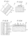
- Figure 1 is an enlarged plan view of a portion of a printed wiring board according to a first embodiment of the present invention.
- Figure 2 is an enlarged sectional view of a portion of a printed wiring board according to a first embodiment of the present invention.
- Figure 3 is an enlarged plan view of a portion of a printed wiring board according to a second embodiment.
- Figure 4 is an enlarged sectional view of a portion of a printed wiring board according to a second embodiment.
- Figure 5 is an enlarged plan view of a portion of a printed wiring board according to a third embodiment of the present invention.
- Figure 6 is an enlarged sectional view of a portion of a printed wiring board according to a third embodiment of the present invention.
- Figure 7 is an enlarged sectional view of a portion of a conventional printed wiring board.
- Fig. 7 shows a conventional printed wiring board 5 which is produced by etching a
copper film 2 on a copper clad laminated plate 1 so as to form desiredcircuit conductors 3 on the upper surface of a base plate 4. On thecircuit conductor 3 of the printed wiring board 5 an overcoat by aninsulating film 6 is formed. The disadvantages of this structure have been disclosed above. - Now, some preferred embodiments of the printed wiring board according to the present invention will be described referring to the drawings. In the drawings, the same reference numeral shows the same or a similar part of a portion thereof for sake of clarity.
- Referring to Figs. 1 and 2 which show a first embodiment of the present invention, a
base 10 and acircuit conductor 11 formed on one surface of thebase plate 10 are shown. On the surface of the circuit conductor 11 aheat radiation film 12 is attached. Theradiation film 12 is formed by painting radiation paste by means e.g. silk screen printing process while producing the printed wiring board, and the paste is hardened. The radiation paste is composed mainly of metal e.g. copper or nickel, or non-organic material e.g. ceramics such as aluminium oxide. - In the illustrated embodiment, a printed wiring board forming
circuit conductor 11 on one surface of thebase plate 10 is shown. However, theradiation film 12 can be applied to other circuit conductors formed on both surfaces of the baseplate or formed as multi-layers conductors. - The illustrated
radiation film 12 is narrower than the width of thecircuit conductor 11. However, theradiation film 12 may have the same width as thecircuit conductor 11. Theradiation film 12 may extend to full length of necessary circuit conductor, or may extend on one or more portions of the circuit conductors as necessary. - In the illustrated embodiment, other construction of the printed wiring board, e.g.
insulating film 6 shown in Fig. 7 is not shown. However, such construction may be added when necessary. - If an insulating film is formed on the
circuit conductor 11, the printedwiring board 13 shown in Figs. 1 and 2 positively dissipates heat produced in thecircuit conductor 11 owing to theradiation film 12 formed on thecircuit conductor 11 so that erroneous operation by overheat is eliminated, and also, heat resistance property of thecircuit conductor 11 is improved by theradiation film 12. - A second embodiment of a printed wiring board is shown in Figs. 3 and 4. As before, on the
base plate 10, theradiation film 12 is formed on theconductor 11. Thecircuit conductor 11 may be formed on one or both surfaces of thebase plate 10. Theradiation film 12 may be smaller than or have the same width as thecircuit conductor 11. - Further, an
insulating film 14 is formed on thecircuit conductor 11 as usual, and aheat dissipating window 15 formed as a slot along a necessary portion or necessary portions of theradiation film 12 is formed through theinsulating film 14. - The above described printed
wiring board 17 according to the second embodiment of the present invention positively dissipates heat produced in thecircuit conductor 11 by theradiation film 12 applied on theconductor 11, and further, as theradiation film 12 is exposed outside by theheat dissipating window 15, heat dissipating property of theradiation film 12 is substantially increased. Consequently, erroneous operation of the printedwiring board 17 owing to overheat of thecircuit conductor 11 by the heat produced in the conductor during operation is effectively eliminated. Further, heat resistance property of thecircuit conductor 11 is improved by theradiation film 12. - A third embodiment of a printed wiring board is shown in Figs. 5 and 6. As before, on the
base plate 10 thecircuit conductor 11 is formed and theradiation film 12 is formed on theconductor 11. Thecircuit conductor 11 may be formed on one or both surfaces of thebase plate 10. Theradiation film 12 may be narrow or have the same width as thecircuit conductor 11. - Further, an
insulating film 14 is formed on thecircuit conductor 11 as usual, and a plurality ofheat dissipating windows 16 having a generally circular or oval circumference and being arranged in a relatively spaced relation along a necessary portion or necessary portions of theradiation film 12, are formed through theinsulating film 14. The number, size and relative space of theheat dissipating windows 16 can be selected as desired considering the heat produced in thecircuit conductor 12 at specific portions. - According to the third embodiment of the present invention the above described printed
wiring board 18 positively dissipates heat produced in thecircuit conductor 11 by theradiation film 12 applied on theconductor 11, and further, as theradiation film 12 is exposed toheat dissipating windows 16, heat dissipating property of theradiation film 12 is substantially increased. Therefore, erroneous operation of the printedwiring board 18 owing to overheat of thecircuit conductor 11 by the heat produced in the conductor during operation is effectively eliminated. Further, heat resistance property of thecircuit conductor 11 is improved by theradiation film 12. - As the
heat dissipating windows 16 do not impair lateral and longitudinal continuity of theinsulation film 14, adhering strength and durability of theinsulation film 14 are not decreased as compared with the slot likewindow 15 shown in Figs. 3 and 4. - As described, according to the present invention, the printed wiring board effectively improves heat dissipating property of the circuit conductor during operation so that erroneous operation owing to overheat of the circuit conductor by the heat produced in the conductor is decreased and heat resistivity of the circuit conductor is improved so that accuracy and service life of the printed wiring board are improved.
Claims (9)
Applications Claiming Priority (6)
| Application Number | Priority Date | Filing Date | Title |
|---|---|---|---|
| JP62235762A JPH0671128B2 (en) | 1987-09-19 | 1987-09-19 | Printed wiring board |
| JP23576387A JPS6477987A (en) | 1987-09-19 | 1987-09-19 | Printed wiring board |
| JP235764/87 | 1987-09-19 | ||
| JP235762/87 | 1987-09-19 | ||
| JP235763/87 | 1987-09-19 | ||
| JP23576487A JPS6480095A (en) | 1987-09-19 | 1987-09-19 | Printed wiring board |
Publications (3)
| Publication Number | Publication Date |
|---|---|
| EP0308576A2 true EP0308576A2 (en) | 1989-03-29 |
| EP0308576A3 EP0308576A3 (en) | 1989-10-18 |
| EP0308576B1 EP0308576B1 (en) | 1994-07-13 |
Family
ID=27332303
Family Applications (1)
| Application Number | Title | Priority Date | Filing Date |
|---|---|---|---|
| EP88105342A Expired - Lifetime EP0308576B1 (en) | 1987-09-19 | 1988-04-02 | A printed wiring board |
Country Status (3)
| Country | Link |
|---|---|
| US (1) | US4859805A (en) |
| EP (1) | EP0308576B1 (en) |
| DE (1) | DE3850626D1 (en) |
Cited By (6)
| Publication number | Priority date | Publication date | Assignee | Title |
|---|---|---|---|---|
| EP0804053A1 (en) * | 1996-04-23 | 1997-10-29 | Robert Bosch Gmbh | Assembly support having at least one heat generating component |
| DE10041829A1 (en) * | 2000-08-25 | 2002-03-21 | Nft Nanofiltertechnik Gmbh | Cooling device used in microprocessors comprises a substrate having a thermal conducting surface that forms a thermal contact with the object to be cooled and a thermal dissipating surface |
| DE10233736B3 (en) * | 2002-07-24 | 2004-04-15 | N F T Nanofiltertechnik Gmbh | heat exchanger device |
| US7044212B1 (en) | 2000-08-25 | 2006-05-16 | Net Nanofiltertechnik Gmbh | Refrigeration device and a method for producing the same |
| US7654308B2 (en) | 2003-10-22 | 2010-02-02 | Nft Nanofiltertechnik Gmbh | Heat exchanger |
| WO2024179957A1 (en) * | 2023-03-02 | 2024-09-06 | Signify Holding B.V. | Means to improve the thermal performance of a printed electronics led light source |
Families Citing this family (6)
| Publication number | Priority date | Publication date | Assignee | Title |
|---|---|---|---|---|
| JP3185682B2 (en) * | 1996-09-19 | 2001-07-11 | 株式会社村田製作所 | Dielectric substrate with heat sink |
| US7804599B2 (en) * | 2008-07-24 | 2010-09-28 | MGM Instruments, Inc. | Fluid volume verification system |
| US8113072B1 (en) | 2009-02-27 | 2012-02-14 | The United States Of America As Represented By The Secretary Of The Navy | Electromagnetic physical scale model modularization system |
| US9113583B2 (en) * | 2012-07-31 | 2015-08-18 | General Electric Company | Electronic circuit board, assembly and a related method thereof |
| US9764313B2 (en) | 2014-06-18 | 2017-09-19 | Basf Corporation | Molecular sieve catalyst compositions, catalyst composites, systems, and methods |
| WO2016157552A1 (en) * | 2015-03-31 | 2016-10-06 | 株式会社棚澤八光社 | Printed board and method for manufacturing same |
Family Cites Families (10)
| Publication number | Priority date | Publication date | Assignee | Title |
|---|---|---|---|---|
| US3530229A (en) * | 1968-09-03 | 1970-09-22 | Ibm | Transmission line cable or the like and terminal connection therefor |
| US3841905A (en) * | 1970-11-19 | 1974-10-15 | Rbp Chem Corp | Method of preparing printed circuit boards with terminal tabs |
| JPS5212463A (en) * | 1975-07-17 | 1977-01-31 | Matsushita Electric Industrial Co Ltd | Printed circuit board |
| DE2904921A1 (en) * | 1979-02-09 | 1980-08-14 | Blaupunkt Werke Gmbh | PRINTED CIRCUIT BOARD |
| FR2480488A1 (en) * | 1980-04-15 | 1981-10-16 | Eaton Manford | Heat conducting and electrically insulating binder - comprising e.g. metal oxide particles in adhesive matrix e.g. silicone used for heat transfer |
| US4385202A (en) * | 1980-09-25 | 1983-05-24 | Texas Instruments Incorporated | Electronic circuit interconnection system |
| US4472762A (en) * | 1980-09-25 | 1984-09-18 | Texas Instruments Incorporated | Electronic circuit interconnection system |
| US4339303A (en) * | 1981-01-12 | 1982-07-13 | Kollmorgen Technologies Corporation | Radiation stress relieving of sulfone polymer articles |
| US4481261A (en) * | 1982-12-01 | 1984-11-06 | Electro Materials Corp. Of America | Blister-resistant dielectric |
| JPS59167096A (en) * | 1983-03-11 | 1984-09-20 | 日本電気株式会社 | Circuit board |
-
1988
- 1988-03-29 US US07/194,841 patent/US4859805A/en not_active Expired - Lifetime
- 1988-04-02 EP EP88105342A patent/EP0308576B1/en not_active Expired - Lifetime
- 1988-04-02 DE DE3850626T patent/DE3850626D1/en not_active Expired - Lifetime
Cited By (8)
| Publication number | Priority date | Publication date | Assignee | Title |
|---|---|---|---|---|
| EP0804053A1 (en) * | 1996-04-23 | 1997-10-29 | Robert Bosch Gmbh | Assembly support having at least one heat generating component |
| DE10041829A1 (en) * | 2000-08-25 | 2002-03-21 | Nft Nanofiltertechnik Gmbh | Cooling device used in microprocessors comprises a substrate having a thermal conducting surface that forms a thermal contact with the object to be cooled and a thermal dissipating surface |
| DE10041829B4 (en) * | 2000-08-25 | 2004-11-04 | N F T Nanofiltertechnik Gmbh | cooler |
| US7044212B1 (en) | 2000-08-25 | 2006-05-16 | Net Nanofiltertechnik Gmbh | Refrigeration device and a method for producing the same |
| DE10233736B3 (en) * | 2002-07-24 | 2004-04-15 | N F T Nanofiltertechnik Gmbh | heat exchanger device |
| US7458416B2 (en) | 2002-07-24 | 2008-12-02 | Nft Nanofiltertechnik Gmbh | Heat-exchanging device |
| US7654308B2 (en) | 2003-10-22 | 2010-02-02 | Nft Nanofiltertechnik Gmbh | Heat exchanger |
| WO2024179957A1 (en) * | 2023-03-02 | 2024-09-06 | Signify Holding B.V. | Means to improve the thermal performance of a printed electronics led light source |
Also Published As
| Publication number | Publication date |
|---|---|
| EP0308576A3 (en) | 1989-10-18 |
| DE3850626D1 (en) | 1994-08-18 |
| US4859805A (en) | 1989-08-22 |
| EP0308576B1 (en) | 1994-07-13 |
Similar Documents
| Publication | Publication Date | Title |
|---|---|---|
| EP0379686B1 (en) | Printed circuit board | |
| EP0308576B1 (en) | A printed wiring board | |
| KR100510383B1 (en) | Controller | |
| EP0324890A1 (en) | Printed wiring board | |
| EP0312682A2 (en) | Printed circuit board | |
| US4925522A (en) | Printed circuit assembly with contact dot | |
| US5739743A (en) | Asymmetric resistor terminal | |
| JP3956516B2 (en) | PCB mounting structure | |
| JPH10178243A (en) | Printed-circuit board provided with heat sink and its manufacture | |
| JP2547861B2 (en) | Method of manufacturing thermal head | |
| JPH10189803A (en) | Mounting structure of insulating substrate for heat dissipating plate | |
| JPS61156754A (en) | High thermal conductive metal base printed substrate | |
| JP3774327B2 (en) | Wiring board | |
| JPH10135589A (en) | Printed substrate and its manufacturing method as well as soldering method of inserted electronic part onto the printed substrate | |
| JPH0691303B2 (en) | Printed wiring board equipment with electronic components | |
| JP3068804B2 (en) | Metal-based multilayer circuit board | |
| US20050206013A1 (en) | Chip module | |
| JPH10150065A (en) | Chip size package | |
| EP0936849A1 (en) | Printed circuit assembly and method of making the same | |
| JP2686829B2 (en) | Hybrid integrated circuit | |
| JPH0671128B2 (en) | Printed wiring board | |
| JP3476927B2 (en) | Thermal head | |
| JP3111227B2 (en) | Printed wiring board for IC card | |
| JPS6039883A (en) | flexible wiring board | |
| JP2684424B2 (en) | Hybrid integrated circuit |
Legal Events
| Date | Code | Title | Description |
|---|---|---|---|
| PUAI | Public reference made under article 153(3) epc to a published international application that has entered the european phase |
Free format text: ORIGINAL CODE: 0009012 |
|
| AK | Designated contracting states |
Kind code of ref document: A2 Designated state(s): BE DE ES FR GB IT NL |
|
| PUAL | Search report despatched |
Free format text: ORIGINAL CODE: 0009013 |
|
| AK | Designated contracting states |
Kind code of ref document: A3 Designated state(s): BE DE ES FR GB IT NL |
|
| 17P | Request for examination filed |
Effective date: 19890927 |
|
| 17Q | First examination report despatched |
Effective date: 19901029 |
|
| GRAA | (expected) grant |
Free format text: ORIGINAL CODE: 0009210 |
|
| AK | Designated contracting states |
Kind code of ref document: B1 Designated state(s): BE DE ES FR GB IT NL |
|
| PG25 | Lapsed in a contracting state [announced via postgrant information from national office to epo] |
Ref country code: IT Free format text: LAPSE BECAUSE OF FAILURE TO SUBMIT A TRANSLATION OF THE DESCRIPTION OR TO PAY THE FEE WITHIN THE PRE;WARNING: LAPSES OF ITALIAN PATENTS WITH EFFECTIVE DATE BEFORE 2007 MAY HAVE OCCURRED AT ANY TIME BEFORE 2007. THE CORRECT EFFECTIVE DATE MAY BE DIFFERENT FROM THE ONE RECORDED.SCRIBED TIME-LIMIT Effective date: 19940713 Ref country code: BE Effective date: 19940713 Ref country code: ES Free format text: THE PATENT HAS BEEN ANNULLED BY A DECISION OF A NATIONAL AUTHORITY Effective date: 19940713 Ref country code: NL Effective date: 19940713 Ref country code: FR Effective date: 19940713 |
|
| REF | Corresponds to: |
Ref document number: 3850626 Country of ref document: DE Date of ref document: 19940818 |
|
| PG25 | Lapsed in a contracting state [announced via postgrant information from national office to epo] |
Ref country code: DE Effective date: 19941014 |
|
| EN | Fr: translation not filed | ||
| NLV1 | Nl: lapsed or annulled due to failure to fulfill the requirements of art. 29p and 29m of the patents act | ||
| PG25 | Lapsed in a contracting state [announced via postgrant information from national office to epo] |
Ref country code: GB Effective date: 19950402 |
|
| PLBE | No opposition filed within time limit |
Free format text: ORIGINAL CODE: 0009261 |
|
| STAA | Information on the status of an ep patent application or granted ep patent |
Free format text: STATUS: NO OPPOSITION FILED WITHIN TIME LIMIT |
|
| 26N | No opposition filed | ||
| GBPC | Gb: european patent ceased through non-payment of renewal fee |
Effective date: 19950402 |
|
| APAH | Appeal reference modified |
Free format text: ORIGINAL CODE: EPIDOSCREFNO |