EP0307210A2 - Appareil enregistreur de mémoire - Google Patents
Appareil enregistreur de mémoire Download PDFInfo
- Publication number
- EP0307210A2 EP0307210A2 EP88308324A EP88308324A EP0307210A2 EP 0307210 A2 EP0307210 A2 EP 0307210A2 EP 88308324 A EP88308324 A EP 88308324A EP 88308324 A EP88308324 A EP 88308324A EP 0307210 A2 EP0307210 A2 EP 0307210A2
- Authority
- EP
- European Patent Office
- Prior art keywords
- memory
- needle
- writing apparatus
- tip portion
- needles
- Prior art date
- Legal status (The legal status is an assumption and is not a legal conclusion. Google has not performed a legal analysis and makes no representation as to the accuracy of the status listed.)
- Withdrawn
Links
Images


Classifications
-
- B—PERFORMING OPERATIONS; TRANSPORTING
- B82—NANOTECHNOLOGY
- B82Y—SPECIFIC USES OR APPLICATIONS OF NANOSTRUCTURES; MEASUREMENT OR ANALYSIS OF NANOSTRUCTURES; MANUFACTURE OR TREATMENT OF NANOSTRUCTURES
- B82Y10/00—Nanotechnology for information processing, storage or transmission, e.g. quantum computing or single electron logic
-
- G—PHYSICS
- G11—INFORMATION STORAGE
- G11B—INFORMATION STORAGE BASED ON RELATIVE MOVEMENT BETWEEN RECORD CARRIER AND TRANSDUCER
- G11B9/00—Recording or reproducing using a method not covered by one of the main groups G11B3/00 - G11B7/00; Record carriers therefor
- G11B9/12—Recording or reproducing using a method not covered by one of the main groups G11B3/00 - G11B7/00; Record carriers therefor using near-field interactions; Record carriers therefor
- G11B9/14—Recording or reproducing using a method not covered by one of the main groups G11B3/00 - G11B7/00; Record carriers therefor using near-field interactions; Record carriers therefor using microscopic probe means, i.e. recording or reproducing by means directly associated with the tip of a microscopic electrical probe as used in Scanning Tunneling Microscopy [STM] or Atomic Force Microscopy [AFM] for inducing physical or electrical perturbations in a recording medium; Record carriers or media specially adapted for such transducing of information
-
- G—PHYSICS
- G11—INFORMATION STORAGE
- G11B—INFORMATION STORAGE BASED ON RELATIVE MOVEMENT BETWEEN RECORD CARRIER AND TRANSDUCER
- G11B21/00—Head arrangements not specific to the method of recording or reproducing
- G11B21/16—Supporting the heads; Supporting the sockets for plug-in heads
- G11B21/20—Supporting the heads; Supporting the sockets for plug-in heads while the head is in operative position but stationary or permitting minor movements to follow irregularities in surface of record carrier
- G11B21/21—Supporting the heads; Supporting the sockets for plug-in heads while the head is in operative position but stationary or permitting minor movements to follow irregularities in surface of record carrier with provision for maintaining desired spacing of head from record carrier, e.g. fluid-dynamic spacing, slider
-
- G—PHYSICS
- G11—INFORMATION STORAGE
- G11B—INFORMATION STORAGE BASED ON RELATIVE MOVEMENT BETWEEN RECORD CARRIER AND TRANSDUCER
- G11B9/00—Recording or reproducing using a method not covered by one of the main groups G11B3/00 - G11B7/00; Record carriers therefor
- G11B9/12—Recording or reproducing using a method not covered by one of the main groups G11B3/00 - G11B7/00; Record carriers therefor using near-field interactions; Record carriers therefor
- G11B9/14—Recording or reproducing using a method not covered by one of the main groups G11B3/00 - G11B7/00; Record carriers therefor using near-field interactions; Record carriers therefor using microscopic probe means, i.e. recording or reproducing by means directly associated with the tip of a microscopic electrical probe as used in Scanning Tunneling Microscopy [STM] or Atomic Force Microscopy [AFM] for inducing physical or electrical perturbations in a recording medium; Record carriers or media specially adapted for such transducing of information
- G11B9/1463—Record carriers for recording or reproduction involving the use of microscopic probe means
- G11B9/149—Record carriers for recording or reproduction involving the use of microscopic probe means characterised by the memorising material or structure
Applications Claiming Priority (8)
| Application Number | Priority Date | Filing Date | Title |
|---|---|---|---|
| JP22736687A JPS6470943A (en) | 1987-09-10 | 1987-09-10 | Memory input device |
| JP227366/87 | 1987-09-10 | ||
| JP24533587A JPS6488938A (en) | 1987-09-29 | 1987-09-29 | Memory input device |
| JP245335/87 | 1987-09-29 | ||
| JP245334/87 | 1987-09-29 | ||
| JP24533487A JPS6488937A (en) | 1987-09-29 | 1987-09-29 | Memory input device |
| JP253157/87 | 1987-10-07 | ||
| JP62253157A JP2673352B2 (ja) | 1987-10-07 | 1987-10-07 | メモリー入力装置 |
Publications (2)
| Publication Number | Publication Date |
|---|---|
| EP0307210A2 true EP0307210A2 (fr) | 1989-03-15 |
| EP0307210A3 EP0307210A3 (fr) | 1991-05-15 |
Family
ID=27477261
Family Applications (1)
| Application Number | Title | Priority Date | Filing Date |
|---|---|---|---|
| EP19880308324 Withdrawn EP0307210A3 (fr) | 1987-09-10 | 1988-09-09 | Appareil enregistreur de mémoire |
Country Status (2)
| Country | Link |
|---|---|
| US (1) | US4945515A (fr) |
| EP (1) | EP0307210A3 (fr) |
Cited By (16)
| Publication number | Priority date | Publication date | Assignee | Title |
|---|---|---|---|---|
| EP0394995A2 (fr) * | 1989-04-25 | 1990-10-31 | Canon Kabushiki Kaisha | Appareil d'enregistrement et de reproduction d'information et milieu d'enregistrement d'information |
| EP0457168A2 (fr) * | 1990-05-16 | 1991-11-21 | BASF Aktiengesellschaft | Procédé pour le marquage d'atomes individuels ou de groupes d'atomes de façon temporellement stable ainsi que l'utilisation de ce procédé pour le stockage d'unités d'information dans le domaine atomique |
| EP0481499A2 (fr) * | 1990-10-19 | 1992-04-22 | Canon Kabushiki Kaisha | Appareil pour l'enregistrement/reproduction par exemple, appareil de mémoire |
| WO1994002939A1 (fr) * | 1992-07-17 | 1994-02-03 | The Penn State Research Foundation | Lecture et ecriture par voie electrochimique d'informations stockees |
| US5434842A (en) * | 1992-07-17 | 1995-07-18 | Biotechnology Research And Development Corporation | Reading and writing stored information by means of electrochemistry |
| WO1997005610A1 (fr) * | 1995-07-28 | 1997-02-13 | International Business Machines Corporation | Applications, dans le stockage de grande capacite, de matrices de sondes locales |
| US5623476A (en) * | 1986-12-24 | 1997-04-22 | Canon Kabushiki Kaisha | Recording device and reproduction device |
| US5835477A (en) * | 1996-07-10 | 1998-11-10 | International Business Machines Corporation | Mass-storage applications of local probe arrays |
| US6208553B1 (en) | 1999-07-01 | 2001-03-27 | The Regents Of The University Of California | High density non-volatile memory device incorporating thiol-derivatized porphyrins |
| US6212093B1 (en) | 2000-01-14 | 2001-04-03 | North Carolina State University | High-density non-volatile memory devices incorporating sandwich coordination compounds |
| US6272038B1 (en) | 2000-01-14 | 2001-08-07 | North Carolina State University | High-density non-volatile memory devices incorporating thiol-derivatized porphyrin trimers |
| US6381169B1 (en) | 1999-07-01 | 2002-04-30 | The Regents Of The University Of California | High density non-volatile memory device |
| US6728129B2 (en) | 2002-02-19 | 2004-04-27 | The Regents Of The University Of California | Multistate triple-decker dyads in three distinct architectures for information storage applications |
| US6777516B2 (en) | 2000-01-14 | 2004-08-17 | North Carolina State University | Substrates carrying polymers of linked sandwich coordination compounds and methods of use thereof |
| US6921475B2 (en) | 2001-03-23 | 2005-07-26 | The Regents Of The University Of California | Open circuit potential amperometry and voltammetry |
| US7042755B1 (en) | 1999-07-01 | 2006-05-09 | The Regents Of The University Of California | High density non-volatile memory device |
Families Citing this family (32)
| Publication number | Priority date | Publication date | Assignee | Title |
|---|---|---|---|---|
| JP2756254B2 (ja) * | 1988-03-25 | 1998-05-25 | キヤノン株式会社 | 記録装置及び再生装置 |
| EP0363147B1 (fr) * | 1988-10-04 | 1996-06-05 | Canon Kabushiki Kaisha | Appareil et procédé d'enregistrement et de reproduction et milieu d'enregistrement pour le procédé d'enregistrement et de reproduction |
| JPH02206043A (ja) * | 1989-02-03 | 1990-08-15 | Olympus Optical Co Ltd | 記憶装置 |
| US5289408A (en) * | 1989-02-09 | 1994-02-22 | Olympus Optical Co., Ltd. | Memory apparatus using tunnel current techniques |
| US5144581A (en) * | 1989-02-09 | 1992-09-01 | Olympus Optical Co., Ltd. | Apparatus including atomic probes utilizing tunnel current to read, write and erase data |
| JP2859715B2 (ja) * | 1989-08-10 | 1999-02-24 | キヤノン株式会社 | 記録媒体用基板及びその製造方法、記録媒体、記録方法、記録再生方法、記録装置、記録再生装置 |
| CA2021582A1 (fr) * | 1989-08-30 | 1991-03-01 | Harris A. Goldberg | Microscope a effet tunnel pour la lecture optique d'un support fluorescent |
| US5144148A (en) * | 1989-11-07 | 1992-09-01 | International Business Machines Corporation | Process for repositioning atoms on a surface using a scanning tunneling microscope |
| DE69127381T2 (de) * | 1990-01-19 | 1998-01-22 | Canon Kk | Informationsverarbeitungssystem und Informationsverarbeitungsmethode |
| JP2945090B2 (ja) * | 1990-07-09 | 1999-09-06 | キヤノン株式会社 | エンコーダ |
| JP2744338B2 (ja) * | 1990-08-01 | 1998-04-28 | キヤノン株式会社 | 情報読取り及び/又は入力を行なう装置及び方法 |
| US5216631A (en) * | 1990-11-02 | 1993-06-01 | Sliwa Jr John W | Microvibratory memory device |
| JP3040887B2 (ja) * | 1992-10-14 | 2000-05-15 | パイオニア株式会社 | 情報記録装置 |
| US5418771A (en) * | 1993-02-25 | 1995-05-23 | Canon Kabushiki Kaisha | Information processing apparatus provided with surface aligning mechanism between probe head substrate and recording medium substrate |
| US5453970A (en) * | 1993-07-13 | 1995-09-26 | Rust; Thomas F. | Molecular memory medium and molecular memory disk drive for storing information using a tunnelling probe |
| US5521774A (en) * | 1994-03-18 | 1996-05-28 | Cartesian Data, Inc. | Memory storage module for storing and accessing |
| US5886922A (en) * | 1997-05-07 | 1999-03-23 | Hewlett-Packard Company | Probe device for memory device having multiple cantilever probes |
| KR100265692B1 (ko) * | 1997-07-03 | 2000-09-15 | 윤덕용 | 에이에프엠을이용한비휘발성메모리소자와해당메모리소자의운영방법 |
| JP3730782B2 (ja) * | 1998-06-29 | 2006-01-05 | パイオニア株式会社 | 光ディスク原盤記録装置 |
| US7260051B1 (en) | 1998-12-18 | 2007-08-21 | Nanochip, Inc. | Molecular memory medium and molecular memory integrated circuit |
| JP4120268B2 (ja) * | 2002-05-27 | 2008-07-16 | 株式会社日立製作所 | 情報記録媒体および情報記録方法 |
| US7233517B2 (en) * | 2002-10-15 | 2007-06-19 | Nanochip, Inc. | Atomic probes and media for high density data storage |
| US6985377B2 (en) | 2002-10-15 | 2006-01-10 | Nanochip, Inc. | Phase change media for high density data storage |
| US20040150472A1 (en) * | 2002-10-15 | 2004-08-05 | Rust Thomas F. | Fault tolerant micro-electro mechanical actuators |
| US6982898B2 (en) * | 2002-10-15 | 2006-01-03 | Nanochip, Inc. | Molecular memory integrated circuit utilizing non-vibrating cantilevers |
| JP4079068B2 (ja) * | 2003-10-17 | 2008-04-23 | 株式会社日立製作所 | 情報記録媒体および情報記録方法 |
| US7379412B2 (en) | 2004-04-16 | 2008-05-27 | Nanochip, Inc. | Methods for writing and reading highly resolved domains for high density data storage |
| US7301887B2 (en) * | 2004-04-16 | 2007-11-27 | Nanochip, Inc. | Methods for erasing bit cells in a high density data storage device |
| US20050232061A1 (en) * | 2004-04-16 | 2005-10-20 | Rust Thomas F | Systems for writing and reading highly resolved domains for high density data storage |
| US7367119B2 (en) | 2005-06-24 | 2008-05-06 | Nanochip, Inc. | Method for forming a reinforced tip for a probe storage device |
| US7463573B2 (en) | 2005-06-24 | 2008-12-09 | Nanochip, Inc. | Patterned media for a high density data storage device |
| US7309630B2 (en) * | 2005-07-08 | 2007-12-18 | Nanochip, Inc. | Method for forming patterned media for a high density data storage device |
Citations (7)
| Publication number | Priority date | Publication date | Assignee | Title |
|---|---|---|---|---|
| US3683337A (en) * | 1969-11-24 | 1972-08-08 | Texas Instruments Inc | Information storage by changing the valence state of a semi-conductor crystal |
| US4489278A (en) * | 1982-06-03 | 1984-12-18 | Tokyo Shibaura Denki Kabushiki Kaisha | Electrostatic voltage detecting device |
| US4575822A (en) * | 1983-02-15 | 1986-03-11 | The Board Of Trustees Of The Leland Stanford Junior University | Method and means for data storage using tunnel current data readout |
| JPS61211849A (ja) * | 1985-03-15 | 1986-09-19 | Matsushita Electric Ind Co Ltd | 記録素子 |
| US4618767A (en) * | 1985-03-22 | 1986-10-21 | International Business Machines Corporation | Low-energy scanning transmission electron microscope |
| EP0205187A2 (fr) * | 1985-06-14 | 1986-12-17 | Sel Semiconductor Energy Laboratory Co., Ltd. | Mémoire à disque optique à cristaux liquides |
| GB2182480A (en) * | 1985-10-31 | 1987-05-13 | Emi Plc Thorn | Information recovery system |
Family Cites Families (2)
| Publication number | Priority date | Publication date | Assignee | Title |
|---|---|---|---|---|
| US4829507A (en) * | 1984-09-14 | 1989-05-09 | Xerox Corporation | Method of and system for atomic scale readout of recorded information |
| US4826732A (en) * | 1987-03-16 | 1989-05-02 | Xerox Corporation | Recording medium |
-
1988
- 1988-09-09 EP EP19880308324 patent/EP0307210A3/fr not_active Withdrawn
- 1988-09-12 US US07/243,512 patent/US4945515A/en not_active Expired - Lifetime
Patent Citations (7)
| Publication number | Priority date | Publication date | Assignee | Title |
|---|---|---|---|---|
| US3683337A (en) * | 1969-11-24 | 1972-08-08 | Texas Instruments Inc | Information storage by changing the valence state of a semi-conductor crystal |
| US4489278A (en) * | 1982-06-03 | 1984-12-18 | Tokyo Shibaura Denki Kabushiki Kaisha | Electrostatic voltage detecting device |
| US4575822A (en) * | 1983-02-15 | 1986-03-11 | The Board Of Trustees Of The Leland Stanford Junior University | Method and means for data storage using tunnel current data readout |
| JPS61211849A (ja) * | 1985-03-15 | 1986-09-19 | Matsushita Electric Ind Co Ltd | 記録素子 |
| US4618767A (en) * | 1985-03-22 | 1986-10-21 | International Business Machines Corporation | Low-energy scanning transmission electron microscope |
| EP0205187A2 (fr) * | 1985-06-14 | 1986-12-17 | Sel Semiconductor Energy Laboratory Co., Ltd. | Mémoire à disque optique à cristaux liquides |
| GB2182480A (en) * | 1985-10-31 | 1987-05-13 | Emi Plc Thorn | Information recovery system |
Non-Patent Citations (2)
| Title |
|---|
| PATENT ABSTRACTS OF JAPAN vol. 11, no. 42 (P-545)(2489) 06 February 1987, & JP-A-61 211849 (MATSUSHITA ELECTRIC INDUSTRIAL CO.) 19 September 1986, * |
| REVIEW OF SCIENTIFIC INSTRUMENTS. vol. 57, no. 2, February 1986, NEW YORK US pages 221 - 224; C.GERBER ET AL: "Scanning Tunneling microscope combined with a scanning electron microscope" * |
Cited By (26)
| Publication number | Priority date | Publication date | Assignee | Title |
|---|---|---|---|---|
| US5623476A (en) * | 1986-12-24 | 1997-04-22 | Canon Kabushiki Kaisha | Recording device and reproduction device |
| EP0394995A2 (fr) * | 1989-04-25 | 1990-10-31 | Canon Kabushiki Kaisha | Appareil d'enregistrement et de reproduction d'information et milieu d'enregistrement d'information |
| EP0394995A3 (fr) * | 1989-04-25 | 1993-03-31 | Canon Kabushiki Kaisha | Appareil d'enregistrement et de reproduction d'information et milieu d'enregistrement d'information |
| US5581537A (en) * | 1989-04-25 | 1996-12-03 | Canon Kabushiki Kaisha | Information record/reproducing apparatus and information recording medium |
| EP0457168A2 (fr) * | 1990-05-16 | 1991-11-21 | BASF Aktiengesellschaft | Procédé pour le marquage d'atomes individuels ou de groupes d'atomes de façon temporellement stable ainsi que l'utilisation de ce procédé pour le stockage d'unités d'information dans le domaine atomique |
| EP0457168A3 (en) * | 1990-05-16 | 1992-08-12 | Basf Aktiengesellschaft | Method for the temporary stable marking of individual atoms or atom groups as well as utilisation of this method for storing information units in the atomic domain |
| EP0481499A2 (fr) * | 1990-10-19 | 1992-04-22 | Canon Kabushiki Kaisha | Appareil pour l'enregistrement/reproduction par exemple, appareil de mémoire |
| EP0481499A3 (en) * | 1990-10-19 | 1993-03-31 | Canon Kabushiki Kaisha | Recording/reproducing apparatus such as a memory apparatus |
| US5396453A (en) * | 1990-10-19 | 1995-03-07 | Canon Kabushiki Kaisha | Recording/reproducing apparatus such as a memory apparatus |
| WO1994002939A1 (fr) * | 1992-07-17 | 1994-02-03 | The Penn State Research Foundation | Lecture et ecriture par voie electrochimique d'informations stockees |
| US5434842A (en) * | 1992-07-17 | 1995-07-18 | Biotechnology Research And Development Corporation | Reading and writing stored information by means of electrochemistry |
| WO1997005610A1 (fr) * | 1995-07-28 | 1997-02-13 | International Business Machines Corporation | Applications, dans le stockage de grande capacite, de matrices de sondes locales |
| US5835477A (en) * | 1996-07-10 | 1998-11-10 | International Business Machines Corporation | Mass-storage applications of local probe arrays |
| US7042755B1 (en) | 1999-07-01 | 2006-05-09 | The Regents Of The University Of California | High density non-volatile memory device |
| US6381169B1 (en) | 1999-07-01 | 2002-04-30 | The Regents Of The University Of California | High density non-volatile memory device |
| US6657884B2 (en) | 1999-07-01 | 2003-12-02 | The Regents Of The University Of California | High density non-volatile memory device |
| US6208553B1 (en) | 1999-07-01 | 2001-03-27 | The Regents Of The University Of California | High density non-volatile memory device incorporating thiol-derivatized porphyrins |
| US7061791B2 (en) | 1999-07-01 | 2006-06-13 | The Regents Of The University Of California | High density molecular memory device |
| US7518905B2 (en) | 1999-07-01 | 2009-04-14 | The Regents Of The University Of California | High density memory device |
| US6212093B1 (en) | 2000-01-14 | 2001-04-03 | North Carolina State University | High-density non-volatile memory devices incorporating sandwich coordination compounds |
| US6272038B1 (en) | 2000-01-14 | 2001-08-07 | North Carolina State University | High-density non-volatile memory devices incorporating thiol-derivatized porphyrin trimers |
| US6451942B1 (en) | 2000-01-14 | 2002-09-17 | North Carolina State University | Substrates carrying polymers of linked sandwich coordination compounds and methods of use thereof |
| US6777516B2 (en) | 2000-01-14 | 2004-08-17 | North Carolina State University | Substrates carrying polymers of linked sandwich coordination compounds and methods of use thereof |
| US6921475B2 (en) | 2001-03-23 | 2005-07-26 | The Regents Of The University Of California | Open circuit potential amperometry and voltammetry |
| US7826250B2 (en) | 2001-03-23 | 2010-11-02 | North Carolina State Univeristy | Open circuit potential amperometry and voltammetry |
| US6728129B2 (en) | 2002-02-19 | 2004-04-27 | The Regents Of The University Of California | Multistate triple-decker dyads in three distinct architectures for information storage applications |
Also Published As
| Publication number | Publication date |
|---|---|
| US4945515A (en) | 1990-07-31 |
| EP0307210A3 (fr) | 1991-05-15 |
Similar Documents
| Publication | Publication Date | Title |
|---|---|---|
| EP0307210A2 (fr) | Appareil enregistreur de mémoire | |
| EP0307211A2 (fr) | Appareil lecteur de mémoire | |
| EP0381113A2 (fr) | Appareil d'enregistrement par courant tunnel avec bras de leviers séparés | |
| US5107112A (en) | Scanning tunnel-current-detecting device and method for detecting tunnel current and scanning tunnelling microscope and recording/reproducing device using thereof | |
| US5220555A (en) | Scanning tunnel-current-detecting device and method for detecting tunnel current and scanning tunnelling microscope and recording/reproducing device using thereof | |
| EP0474433B1 (fr) | Procédé et appareil pour traiter des informations | |
| EP0437275A2 (fr) | Microsonde, méthode pour sa réalisation et appareil d'entrée et de sortie de données l'utilisant | |
| JPH02123541A (ja) | 間隔制御トンネリング変換器 | |
| US5214342A (en) | Two-dimensional walker assembly for a scanning tunneling microscope | |
| EP0481499A2 (fr) | Appareil pour l'enregistrement/reproduction par exemple, appareil de mémoire | |
| US5371728A (en) | Information recording/reproducing apparatus using probe | |
| KR100407202B1 (ko) | 원자표면또는다른파상표면을주사하는스캐닝터널링현미경의센서또는기타센서의나노미터단위의실시간위치측정방법및장치 | |
| EP0431623B1 (fr) | Méthode et appareil de façonnement d'une sonde | |
| EP0398334A1 (fr) | Appareil pour la détection d'une position | |
| EP0435645B1 (fr) | Milieu d'enregistrement, procédé d'enregistrement et procédé de lecture | |
| US5199021A (en) | Method of access to recording medium, and apparatus and method for processing information | |
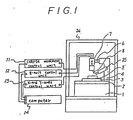
| JP2673352B2 (ja) | メモリー入力装置 | |
| US5255259A (en) | Method of access to recording medium, and apparatus and method for processing information | |
| JP2673351B2 (ja) | メモリー出力装置 | |
| JP2673352C (fr) | ||
| JP3053971B2 (ja) | トンネル電流発生用三次元変位素子、該トンネル電流発生用三次元変位素子を用いたマルチ探針ユニット、および情報処理装置 | |
| JP2789244B2 (ja) | 微小プローブの形成方法 | |
| JPH0540968A (ja) | 記録及び/又は再生装置 | |
| JP2995126B2 (ja) | 情報処理装置 | |
| JP2942011B2 (ja) | 情報記憶装置 |
Legal Events
| Date | Code | Title | Description |
|---|---|---|---|
| PUAI | Public reference made under article 153(3) epc to a published international application that has entered the european phase |
Free format text: ORIGINAL CODE: 0009012 |
|
| AK | Designated contracting states |
Kind code of ref document: A2 Designated state(s): DE FR GB |
|
| PUAL | Search report despatched |
Free format text: ORIGINAL CODE: 0009013 |
|
| AK | Designated contracting states |
Kind code of ref document: A3 Designated state(s): DE FR GB |
|
| STAA | Information on the status of an ep patent application or granted ep patent |
Free format text: STATUS: THE APPLICATION IS DEEMED TO BE WITHDRAWN |
|
| 18D | Application deemed to be withdrawn |
Effective date: 19911118 |