EP0307065A2 - Commande de lampe à décharge - Google Patents
Commande de lampe à décharge Download PDFInfo
- Publication number
- EP0307065A2 EP0307065A2 EP88301911A EP88301911A EP0307065A2 EP 0307065 A2 EP0307065 A2 EP 0307065A2 EP 88301911 A EP88301911 A EP 88301911A EP 88301911 A EP88301911 A EP 88301911A EP 0307065 A2 EP0307065 A2 EP 0307065A2
- Authority
- EP
- European Patent Office
- Prior art keywords
- voltage source
- load
- power
- resonant circuit
- circuit
- Prior art date
- Legal status (The legal status is an assumption and is not a legal conclusion. Google has not performed a legal analysis and makes no representation as to the accuracy of the status listed.)
- Withdrawn
Links
Images
Classifications
-
- H—ELECTRICITY
- H05—ELECTRIC TECHNIQUES NOT OTHERWISE PROVIDED FOR
- H05B—ELECTRIC HEATING; ELECTRIC LIGHT SOURCES NOT OTHERWISE PROVIDED FOR; CIRCUIT ARRANGEMENTS FOR ELECTRIC LIGHT SOURCES, IN GENERAL
- H05B41/00—Circuit arrangements or apparatus for igniting or operating discharge lamps
- H05B41/14—Circuit arrangements
- H05B41/36—Controlling
- H05B41/38—Controlling the intensity of light
- H05B41/39—Controlling the intensity of light continuously
- H05B41/392—Controlling the intensity of light continuously using semiconductor devices, e.g. thyristor
-
- H—ELECTRICITY
- H05—ELECTRIC TECHNIQUES NOT OTHERWISE PROVIDED FOR
- H05B—ELECTRIC HEATING; ELECTRIC LIGHT SOURCES NOT OTHERWISE PROVIDED FOR; CIRCUIT ARRANGEMENTS FOR ELECTRIC LIGHT SOURCES, IN GENERAL
- H05B41/00—Circuit arrangements or apparatus for igniting or operating discharge lamps
- H05B41/14—Circuit arrangements
- H05B41/26—Circuit arrangements in which the lamp is fed by power derived from dc by means of a converter, e.g. by high-voltage dc
- H05B41/28—Circuit arrangements in which the lamp is fed by power derived from dc by means of a converter, e.g. by high-voltage dc using static converters
- H05B41/282—Circuit arrangements in which the lamp is fed by power derived from dc by means of a converter, e.g. by high-voltage dc using static converters with semiconductor devices
- H05B41/285—Arrangements for protecting lamps or circuits against abnormal operating conditions
-
- Y—GENERAL TAGGING OF NEW TECHNOLOGICAL DEVELOPMENTS; GENERAL TAGGING OF CROSS-SECTIONAL TECHNOLOGIES SPANNING OVER SEVERAL SECTIONS OF THE IPC; TECHNICAL SUBJECTS COVERED BY FORMER USPC CROSS-REFERENCE ART COLLECTIONS [XRACs] AND DIGESTS
- Y02—TECHNOLOGIES OR APPLICATIONS FOR MITIGATION OR ADAPTATION AGAINST CLIMATE CHANGE
- Y02B—CLIMATE CHANGE MITIGATION TECHNOLOGIES RELATED TO BUILDINGS, e.g. HOUSING, HOUSE APPLIANCES OR RELATED END-USER APPLICATIONS
- Y02B20/00—Energy efficient lighting technologies, e.g. halogen lamps or gas discharge lamps
Definitions
- This invention relates to a method and apparatus for driving discharge lamps. More particularly, the present invention deals with the problems associated with the driving of discharge lamps such as flourescent, arc and neon lamps, in an efficient and effective manner throughout the complex operating cycle of these devices.
- the shortening of life attributed to the number of starts is explained by the fact that during starting, the higher voltage that the lamp must withstand before effective cathode emission is established, causes some of the emission material on the cathode to be consumed. Once all the emission material is gone the cathode itself begins to deteriorate until eventually the entire cathode is gone and the lamp will fail to ignite.
- Another factor that contributes to lamp deterioration is the frequency of current reversal in the lamp.
- a first object of the present invention is to maximize the luminous efficiency of a discharge lamp and its associated electronic driving apparatus. This is accomplished through the power sourcing characteristic of the driver, by causing the required power to be dissipated while maintaining the power factor in the lamp as near unity as possible with the real components available for the implementation of the apparatus.
- a second object of the present invention is to provide a driving apparatus which is simple and inexpensive to manufacture. This can be accomplished by selecting components that are restricted to mature technology, that are cheap and readily available.
- a third object of the present invention is to increase the life of discharge lamps that are being driven. This accomplished by minimizing the damage to the lamp during start-up and during subsequent operation. Lamp life is extended by allowing the discharge lamps to be started very quickly by simultaneously applying cathode heat and increasingly potential across the lamp.
- the potential across the lamp is not limited by the source of potential of the power supply so the driver is capable of providing within its design limits whatever potential is required to ignite the lamp. In practice, even temperatures below 20°C, start-ups virtually instaneous and flicker free have been demonstrated. In the low temperature test and at ordinary temperatures, no evidence of tube damage such as blackening of cathode areas has been observed.
- the life of discharged lamps can be extended by operating the driver at a much higher frequency than the ordinary control gear.
- the frequency is chosen to be high enough that there is insufficient time for the emission material on the cathodes to cool to the point where a mini restart would be necessary. At these frequencies, the lamp impedance appears as a pure resistance even immediately after current reversal.
- the lamp life is also affected by the crest factor of the current in that it is forced to conduct.
- the apparatus of the present invention causes the current in the lamp to be sinusoidal and symetrical in both directions without any DC offset. This insures that the cathode wear will be minimized and uniformed on both ends.
- a fourth object of the present invention is to provide a driving apparatus which allows safe removal of a discharge lamp when damaged or burnt out. This is achieved by designing the apparatus such that the lamp is made a necessary component for sustained operation, such that if the lamp is removed or damaged, operation will cease, thus avoiding the danger of maintaining excessive voltages on lamp socket while the lamp is being replaced or waiting to be exchanged.
- a provision for signal level enabling and disabling of driver operation has been provided. Ths is useful for providing an alternative means to prevent overheating or to disable the unit for whatever other reason may be deemed necessary.
- a fifth object of the present invention is to provide a driving apparatus adapted to minimize the unwanted side effects created when operating discharge lamps. This has been achieved by providing a driver operated from a DC source thereby creating a driver which is virtually flicker free. Any stroboscopic effect that may be present is at a frequency 30 to 100 times higher than presently common. Further, at these frequencies, even if the effect were humanly perceivable, it would be considerably attenuated by the persistence of even inexpensive phosphors. Acoustic noise, is at a frequency twice the operating frequency of the driver well beyond the ability of people's hearing.
- frequencies of 50,000 to 100,000 cylces per second (which would commonly be the case with the driver) air and construction materials form a very poor medium for efficient transmission, and form an effective means to attenuate what little imperceivable acoustic noise may escape.
- a first aspect of the present invention is to provide an apparatus for driving a discharge lamp having a pair of cathodes and a pair of anodes comprising resonant circuit means connected in series with said discharge lamp, switching means connected between a negative and positive voltage source adapted to alternately connect said resonant circuit means thereto, reactive circuit means connected across said discharge lamp adapted to produce a high voltage across said lamp, synchronising circuit means for driving said switching means, said synchronizing circuit means being connected to said switching means and said discharge lamp, and control circuit means for controlling the amount of energy drawn from said voltage source.
- a method of driving a load to dissipate a predetermined amount of power using a power sourcing apparatus having resonant circuit means incorporating said load, switching means connected between a negative and positive voltage source adapted to alternatively connect said resonant circuit means thereto, synchronizing means for driving said switching means, said synchronizing means being connected to said switching means and said resonant circuit means, and control means for controlling the amount of energy drawn from said voltage source, comprising the steps of: detecting a zero current state at said switching means by means of said synchronizing means; actuating said switching means to drive said resonant circuit means between said negative and positive voltage source when said zero current state is detected; actuating said control means when said resonant circuit means is connected to said positive voltage source to allow a predetermined amount of charge to be absorbed from said negative voltage source; actuating said control means when said resonant circuit means is connected to said negative voltage source to allow a predetermined amount
- the driving method and apparatus that are the subject of this disclosure do not limit the power delivered to the lamp, as is the case with the ballast but rather cause the lamp to dissipate the required power. Therefore, a more appropriate term to describe the operation is “driving" the lamp.
- the discharge lamp driving apparatus will be referred in this disclosure as the “lamp driver” or simply the “driver”.
- the techniques used to cause the lamp to dissipate the required power will be referred to as "drive requirements”.
- the discharge lamp is one illustration of this type of load. Initially the discharge lamp appears as an open circuit and until the voltage applied across it is high enough, it does not conduct. Once conduction is initiated and current begins to flow, the impedance of the device begins to drop, exhibiting a negative impedance characteristic. In order for a discharge lamp to provide the intended light output it must dissipate a required amount of power. But the control gear that is normally in use with this type of load is of the current source type, therefore the actual power consumed depends more on the lamp then on the control gear's ability to supply the power. The actual power consumed by the lamp will then depend on: the manufacturing tolerances, the ambient conditions, and on the drift in bulb parameters as a consequence of aging.
- control gear were used where the power supplied to the lamp were independent of the above-mentioned variables in the lamp, then the lamp would be forced (or driven to dissipate the required power and consequently provide the intended light output.
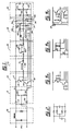
- the driving apparatus is basically comprised of an EMI filtering circuit 10 and AC to DC convertor 11, a switching circuit 12, a resonant circuit 13, a load 14, a synchronizing circuit 15 and an energy control circuit 16.
- the EMI filter circuit 10 is necessary in virtually all high frequency equipment to prevent high frequency interference from being conducted back into the utility supply lines or the local supply which may be shared by sensitive equipment.
- the driver apparatus by its nature produces low energy emissions for a given amount of power then conversion topologies commonly in use. Therefore, the requirements of this circuit are less stringent than otherwise might be the case. However, both AC and DC power sources may require that this circuit be present.
- a low pass filter looking in the direction of the line is depicted. If more filtering is required, a large variety of known filter configurations may be used as well.
- Diodes 30 and 31 and capacitors 32 and 33 of AC to DC convertor circuit 11 form a rectifier and filter which is the DC supply for the driving apparatus.
- the AC to DC convertor circuit 11 is only required if the driver has to be operated on an AC system.
- the basic driver DC therefore other than producing the required DC, the other objective of this circuit is related to the practical considerations in real applications.
- the rms current drawn from the supply and the phase angle are related to the practical considerations in real applications.
- the AC to DC convertor circuit shown in Figure 2 would be more desirable since the crest factor of the current required to charge the filter capacitor is controlled at a lower value, and also the characteristic of the power factor is mainly non-reactive. This is particularly desirable on distribution systems where there is a significant lagging reactive power factor present.
- the effect is, that during the earlier part of the cycle, the circuit configuration will be taking power from the reactive energy being forced into the power line by the inductively reactive equipment during the early part of each cycle. The net effect being that from the point of view of the utility there is a improvement in the power factor of the total load.
- the switching circuit 12 is comprised of the electrical switching elements which will alternately connect the series resonant circuit 13 to the positive and negative rails 17 and 18 as dictated by the synchronizing circuit 15.
- the implementation may be in semi-conductor form such as by the use of bipolar or mos transistors or even mechanical switches. The choice will affect the operating frequency and the design of the synchronizing circuit 15.
- Figures 3a, 3b and 3c depict some of these possibilities.
- Figure 3c shows that the switching circuit can incorporate a transformer 19 if the output voltage required is to be something different than available.
- the circuit shown in Figure 3c is a vertical push-pull using cascade driven bipolar transistors.
- One of the advantages of using this circuit design is that it offers a low end to end capacity in transformers that are bifi liar would since the two windings are in phase, resulting in higher efficiency at high voltage, high frequency operation and low manufacturing cost.
- the resonant circuit 13 is basically comprised of a series LC circuit. This forms a major part of the frequency determining components.
- the inductor 20 is the main inductance in the system whereas a capacitor 21 is one of several but is the dominant one. Capacitor 21 is also responsible for the very high current power sourcing characteristic at low load impedance conditions. Further, the capacitor or some equivalent of it, is always required or else the power control circuitry 16 will not operate properly. If the power sourcing characteristics is to be maintained, no DC path can be allowed through the frequency determining elements.
- the load 14 is comprised of a discharge lamp 22 and a reactive element 23 to produce the very high voltage characteristic of a power source at high load impedance or open circuit conditions.
- the reactances may be either capacitive or inductive depending on whether the frequency of operation during near open circuit conditions need to be raised or lowered. This reactance will also effect the operating frequency of the system and is therefore the other major frequency determining element in the system.
- the reactance is shown in conjunction with the load because the choice of type (inductive or capacitive) and specific value depends very heavily on the type of load to be driven.
- a discharge lamp such as a neon lamp, used as a load
- a parallel reactance so that power will be available to the load when the load voltage is much higher than the available voltage at the switch, both to start and if desired to operate the load.
- the choice may be of either type.
- the ratio to the main resonating capacitor is application dependent. However, the choice will effect the operating frequency and therefore the final operating frequency will be the result of the two reactances chosen.
- the voltage across the main resonating capacitor should be at least 1.4 times the anticipated voltage across the load.
- a parallel reactance will be required that will result in a parallel equivalent impedance which will allow the equivalence series resonant current to be higher than intended load current.
- the criteria being that the product of the load voltage times the load current be equal to the available source voltage at the switch times the equivalent series resonant current.
- the synchronizing circuit 15 also includes a start-up circuit 24.
- the starting circuit may be any impulse generator which will shut off once the circuit is operating.
- the start up circuit shown at 24 is for illustrative purposes only and it is not necessarily limited to that embodiment.
- the synchronizing circuit accomplishes several important functions. First it is responsible for operating the switching circuit 12 as near to zero current as possible. Second, it must drive the switching circuit depending on the type, such that commutation will take place as close to the zero current condition as possible.
- the synchronizing circuit 15 depicts for this function a transformer 25.
- the design of the transformer in this case must take into account the delay time of the switching element 17 and 18 used such that switching coincidence occurs at zero current.
- the synchronizing element must also provide the necessary drive power to the switches. The requirement for driving MOS up is quite different than cascade driving by polar transistors. The design of the circuit will depend on the switching elements chosen.
- the energy control circuit 16 controls the amount of energy that is drawn from the power supply during each half cycle of the discharge lamp. This function is accomplished by metering a certain desired charge into a reactive component and when the desired charge level is reached, recirculation of power is initiated to prevent current from flowing from the power supply, thus preventing any further energy drop. Provided that no DC path exists through the frequency determining components and the major frequency determining capacitor as a voltage across it at least 1.4 times the load voltage, then the energy control mechanism will have virtually negligible effect on the operating frequency.
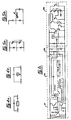
- FIG. 5a and 5b Other embodiments of the control circuit are shown in Figures 5a and 5b. The most complex of these is shown in Figure 6 at reference numeral 26.
- the circuit depicts an integradable divider and driver for an MOS switch.
- the circuit takes a reference value set on the variable resistor 48 and correlates to the supply voltage, such that if the supply voltage doubles, the current drawn is reduced to 1/2, thereby providing a programmable constant power, power source and convertor.
- the point of connection of the variable resistor 48 could also be used for remote programming or for closed loop feedback operation.
- the control circuit 26 may be used because the power control scheme has negligible effect on the operating frequency. In addition, regardless of the activity within the control circuit, the voltage and current through the load remains sinusoidal.
- the schematic diagram illustrated in Figure 6 is a more complex but more efficient discharge lamp driver. It is comprised of the vertical push-pull switching circuit 27 also shown in Figure 3c. Circuit 28 is basically comprised of a dual resonant circuit combined by the means of a t-transformer used as a dual fluorescent driver. A start-up circuit 29 is also used and is similar to start-up circuit 24 shown in Figure 1.
- Resistor 34 and zener diode 35 form a voltage reference at the cathode of zener diode 35.
- Component 37 forms a trigger device called a PUT.
- the anode 28 of trigger device 37 is connected to capacitor 39 which is charged through resistor 40 forming a time constant such that when the voltage to the anode of trigger device is high enough to conduct, it will cause the PUT to fire and thus supply a pulse of energy to turn on the transistor 41.
- the transistor Once the transistor is conducting, current will flow through the series resonant tank circuit comprised of conductor 20, capacitor 21, capacitor 23, transformer 25, and capacitors 42 and 43.
- Discharge lamp 22 is not yet ignited and therefore appears as an open circuit across capacitor 23.
- the cathodes of lamp 22 are in series with both ends of capacitor 23 and thus serve to complete the series circuit.
- transformer 25 would conduct no current, thus preventing transistor 41 from being latched into the on-state. This mechanism then acts to prevent the circuit from starting in the case of an absent or faulty lamp or if during operation the lamp would be removed, operation will also cease. Therefore, the cathode elements of lamp 22 are necessary components for sustained operation.
- the latching of transistor 41 to the on-state constitutes a step function applied to the series resonant circuit.
- the resulting transient will cause the voltage between inductor 20 and capacitor 21 to peak in the positive direction when the current in the series circuit reaches 0.
- current transformer 25 will no longer be able to sustain drive to transistor 41.
- the magnetizing current in current transformer 25 together with the imminent current reversal in the series resonant circuit will cause transistor 44 to be turned on while the emitter of transistor 41 becomes reversed biased and is thus shut off.
- Transistor 33 now becomes latched on by the drive transformer 25, which is designed to provide a drive current sufficient to maintain saturation by providing a base current proportional in this case to the emittor current of transistor 44.
- the power source supply accomplishes the fluorescent light ignition sequence.
- lamp 22 begins to conduct current, its now resistive impedance is in parallel with capacitor 23, effectively changing the equivalent series resonant frequency. Since the driver transistors 41 and 44 are synchronized by transformer 25, the subsequent driving will maintain operation at the maximum Q. As the current in lamp 22 increases due to negative impedance charac teristic, capacitor 23 is more and more bypassed thus further lowering the operating frequency, until when full conduction in the lamp is reached, the dominant frequency determining elements become inductor 20 and capacitor 21 and the resonant frequency is only slightly affected by the parallel combination of lamp 22 and capacitor 23 (which now appears predominantly resistive).
- diodes 46 and 47 limit the energy
- the self-synchronising process always maintains resonance thus the total impedance of the reactive elements in the series circuit is cancelled. Therefore, from the point of view of the lamp, aside from the non-linearities of the components used, there is no series impedance effectively limiting the current or voltage applied to the lamp. Since there is no effective series impedance, ballasting does not take place in the conventional sense, but the lamp is forced to dissipate all of the energy which is drawn from the power supply during each half cycle. Accordingly, the present driving apparatus provides the characteristics of a nearly ideal power source, namely, very high voltage at high impedance and very high current at short circuit.
Applications Claiming Priority (2)
| Application Number | Priority Date | Filing Date | Title |
|---|---|---|---|
| CA546491 | 1987-09-09 | ||
| CA546491 | 1987-09-09 |
Publications (2)
| Publication Number | Publication Date |
|---|---|
| EP0307065A2 true EP0307065A2 (fr) | 1989-03-15 |
| EP0307065A3 EP0307065A3 (fr) | 1989-08-30 |
Family
ID=4136408
Family Applications (1)
| Application Number | Title | Priority Date | Filing Date |
|---|---|---|---|
| EP88301911A Withdrawn EP0307065A3 (fr) | 1987-09-09 | 1988-03-04 | Commande de lampe à décharge |
Country Status (10)
| Country | Link |
|---|---|
| US (1) | US4933606A (fr) |
| EP (1) | EP0307065A3 (fr) |
| JP (1) | JPS6472495A (fr) |
| KR (1) | KR890006110A (fr) |
| CN (1) | CN1035407A (fr) |
| AU (1) | AU600348B2 (fr) |
| BR (1) | BR8804589A (fr) |
| DK (1) | DK498788A (fr) |
| FI (1) | FI884128A (fr) |
| NO (1) | NO884003L (fr) |
Cited By (4)
| Publication number | Priority date | Publication date | Assignee | Title |
|---|---|---|---|---|
| EP0395776A1 (fr) * | 1989-05-02 | 1990-11-07 | Siemens Aktiengesellschaft | Ballast électrique |
| EP0618753A2 (fr) * | 1993-03-29 | 1994-10-05 | Ultra-Lum, Inc. | Ballast électronique pour des appareils d'éclairage par transmission et de réticulation |
| EP1021072A1 (fr) * | 1999-01-16 | 2000-07-19 | Hella KG Hueck & Co. | Ballast pour une lampe à décharge d'un véhicule |
| WO2005046038A1 (fr) | 2003-11-10 | 2005-05-19 | The University Of Hong Kong | Ballast a intensite reglable a entree resistive et faible niveau d'interference electromagnetique |
Families Citing this family (6)
| Publication number | Priority date | Publication date | Assignee | Title |
|---|---|---|---|---|
| GB2264596B (en) * | 1992-02-18 | 1995-06-14 | Standards Inst Singapore | A DC-AC converter for igniting and supplying a gas discharge lamp |
| US5500575A (en) * | 1993-10-27 | 1996-03-19 | Lighting Control, Inc. | Switchmode AC power controller |
| US6034488A (en) * | 1996-06-04 | 2000-03-07 | Lighting Control, Inc. | Electronic ballast for fluorescent lighting system including a voltage monitoring circuit |
| SG68587A1 (en) * | 1996-07-27 | 1999-11-16 | Singapore Productivity And Sta | An electronic ballast circuit |
| US7126450B2 (en) * | 1999-06-21 | 2006-10-24 | Access Business Group International Llc | Inductively powered apparatus |
| US9320115B2 (en) * | 2010-11-30 | 2016-04-19 | The Sloan Company, Inc. | Power control unit |
Citations (5)
| Publication number | Priority date | Publication date | Assignee | Title |
|---|---|---|---|---|
| US4346332A (en) * | 1980-08-14 | 1982-08-24 | General Electric Company | Frequency shift inverter for variable power control |
| EP0075176A2 (fr) * | 1981-09-18 | 1983-03-30 | Oy Helvar | Ballast électronique pour lampes à décharge |
| US4461980A (en) * | 1982-08-25 | 1984-07-24 | Nilssen Ole K | Protection circuit for series resonant electronic ballasts |
| WO1985001400A1 (fr) * | 1983-09-19 | 1985-03-28 | Minitronics Pty. Limited | Reduction a un minimum de la teneur en harmoniques pour des inverseurs a semi-conducteurs fonctionnant sur le secteur et attaquant des tubes a decharge gazeuse |
| EP0205287A2 (fr) * | 1985-06-04 | 1986-12-17 | Thorn Emi Lighting (Nz) Limited | Alimentations de puissance à commutation |
Family Cites Families (4)
| Publication number | Priority date | Publication date | Assignee | Title |
|---|---|---|---|---|
| US4207497A (en) * | 1978-12-05 | 1980-06-10 | Lutron Electronics Co., Inc. | Ballast structure for central high frequency dimming apparatus |
| US4554487A (en) * | 1983-05-17 | 1985-11-19 | Nilssen Ole K | Electronic fluorescent lamp ballast with overload protection |
| JPH0412636Y2 (fr) * | 1985-04-18 | 1992-03-26 | ||
| US4728866A (en) * | 1986-09-08 | 1988-03-01 | Lutron Electronics Co., Inc. | Power control system |
-
1988
- 1988-03-04 EP EP88301911A patent/EP0307065A3/fr not_active Withdrawn
- 1988-03-15 JP JP63059565A patent/JPS6472495A/ja active Pending
- 1988-03-24 AU AU13710/88A patent/AU600348B2/en not_active Ceased
- 1988-09-06 BR BR8804589A patent/BR8804589A/pt unknown
- 1988-09-08 DK DK498788A patent/DK498788A/da not_active Application Discontinuation
- 1988-09-08 FI FI884128A patent/FI884128A/fi not_active IP Right Cessation
- 1988-09-08 NO NO88884003A patent/NO884003L/no unknown
- 1988-09-09 KR KR1019880011689A patent/KR890006110A/ko not_active Application Discontinuation
- 1988-09-09 CN CN88106611A patent/CN1035407A/zh active Pending
-
1989
- 1989-02-15 US US07/310,465 patent/US4933606A/en not_active Expired - Fee Related
Patent Citations (5)
| Publication number | Priority date | Publication date | Assignee | Title |
|---|---|---|---|---|
| US4346332A (en) * | 1980-08-14 | 1982-08-24 | General Electric Company | Frequency shift inverter for variable power control |
| EP0075176A2 (fr) * | 1981-09-18 | 1983-03-30 | Oy Helvar | Ballast électronique pour lampes à décharge |
| US4461980A (en) * | 1982-08-25 | 1984-07-24 | Nilssen Ole K | Protection circuit for series resonant electronic ballasts |
| WO1985001400A1 (fr) * | 1983-09-19 | 1985-03-28 | Minitronics Pty. Limited | Reduction a un minimum de la teneur en harmoniques pour des inverseurs a semi-conducteurs fonctionnant sur le secteur et attaquant des tubes a decharge gazeuse |
| EP0205287A2 (fr) * | 1985-06-04 | 1986-12-17 | Thorn Emi Lighting (Nz) Limited | Alimentations de puissance à commutation |
Cited By (8)
| Publication number | Priority date | Publication date | Assignee | Title |
|---|---|---|---|---|
| EP0395776A1 (fr) * | 1989-05-02 | 1990-11-07 | Siemens Aktiengesellschaft | Ballast électrique |
| EP0618753A2 (fr) * | 1993-03-29 | 1994-10-05 | Ultra-Lum, Inc. | Ballast électronique pour des appareils d'éclairage par transmission et de réticulation |
| EP0618753A3 (en) * | 1993-03-29 | 1995-11-29 | Ultra Lum Inc | Electronic ballast for transilluminators and crosslinkers. |
| EP1021072A1 (fr) * | 1999-01-16 | 2000-07-19 | Hella KG Hueck & Co. | Ballast pour une lampe à décharge d'un véhicule |
| US6300726B1 (en) | 1999-01-16 | 2001-10-09 | Hella Kg Hueck & Co. | Ballast for high-pressure gas discharge lamp |
| WO2005046038A1 (fr) | 2003-11-10 | 2005-05-19 | The University Of Hong Kong | Ballast a intensite reglable a entree resistive et faible niveau d'interference electromagnetique |
| EP1683256A1 (fr) * | 2003-11-10 | 2006-07-26 | The University of Hong Kong | Ballast a intensite reglable a entree resistive et faible niveau d'interference electromagnetique |
| EP1683256A4 (fr) * | 2003-11-10 | 2010-11-24 | Univ Hong Kong | Ballast a intensite reglable a entree resistive et faible niveau d'interference electromagnetique |
Also Published As
| Publication number | Publication date |
|---|---|
| CN1035407A (zh) | 1989-09-06 |
| FI884128A (fi) | 1989-03-10 |
| JPS6472495A (en) | 1989-03-17 |
| EP0307065A3 (fr) | 1989-08-30 |
| KR890006110A (ko) | 1989-05-18 |
| NO884003L (no) | 1989-03-10 |
| FI884128A0 (fi) | 1988-09-08 |
| US4933606A (en) | 1990-06-12 |
| AU600348B2 (en) | 1990-08-09 |
| NO884003D0 (no) | 1988-09-08 |
| AU1371088A (en) | 1989-03-09 |
| DK498788A (da) | 1989-03-10 |
| DK498788D0 (da) | 1988-09-08 |
| BR8804589A (pt) | 1989-04-11 |
Similar Documents
| Publication | Publication Date | Title |
|---|---|---|
| US5612597A (en) | Oscillating driver circuit with power factor correction, electronic lamp ballast employing same and driver method | |
| US6339298B1 (en) | Dimming ballast resonant feedback circuit | |
| US7750580B2 (en) | Dimmable, high power factor ballast for gas discharge lamps | |
| US7061188B1 (en) | Instant start electronic ballast with universal AC input voltage | |
| US6037722A (en) | Dimmable ballast apparatus and method for controlling power delivered to a fluorescent lamp | |
| EP1675442A2 (fr) | Ballast avec circuit de préchauffage des filaments | |
| KR100741253B1 (ko) | 고압 방전 램프 안정기 회로 | |
| EP1286574B1 (fr) | Ballast avec préchauffage efficace des filaments et protection contre les défauts de lampe | |
| US5084653A (en) | Power-line-isolated dimmable electronic ballast | |
| JP4700289B2 (ja) | 負荷の電力消費の調整方法、負荷の電力消費の調整回路およびランプ用の電気点灯装置 | |
| WO1998027791A1 (fr) | Circuit de ballaste a retour magnetique pour lampe fluorescente | |
| CN101960924B (zh) | 可调光瞬时启动镇流器 | |
| US6815908B2 (en) | Dimmable self-oscillating electronic ballast for fluorescent lamp | |
| EP1050196B1 (fr) | Circuit de convertisseur auto-oscillant | |
| Tao et al. | Self-oscillating electronic ballast with dimming control | |
| US4933606A (en) | Discharge lamp driving method and electronic operators for implementation of the same | |
| Orletti et al. | HID lamp electronic ballast with reduced component number | |
| US20030230990A1 (en) | Electronic ballast using cut & save technology | |
| US7122972B2 (en) | Dimmable ballast with resistive input and low electromagnetic interference | |
| KR0169164B1 (ko) | 순간점등형 형광램프 점등회로 | |
| US8288956B1 (en) | Lamp preheat circuit for a program start ballast with filament voltage cut-back in steady state | |
| US8354795B1 (en) | Program start ballast with true parallel lamp operation | |
| US20070164685A1 (en) | Discharge lamp lighting apparatus | |
| JP3315385B2 (ja) | 蛍光ランプ点灯装置 | |
| JP2002015884A (ja) | 高圧放電灯用電子式安定器 |
Legal Events
| Date | Code | Title | Description |
|---|---|---|---|
| PUAI | Public reference made under article 153(3) epc to a published international application that has entered the european phase |
Free format text: ORIGINAL CODE: 0009012 |
|
| AK | Designated contracting states |
Kind code of ref document: A2 Designated state(s): AT BE CH DE ES FR GB GR IT LI LU NL SE |
|
| PUAL | Search report despatched |
Free format text: ORIGINAL CODE: 0009013 |
|
| AK | Designated contracting states |
Kind code of ref document: A3 Designated state(s): AT BE CH DE ES FR GB GR IT LI LU NL SE |
|
| 17P | Request for examination filed |
Effective date: 19900123 |
|
| STAA | Information on the status of an ep patent application or granted ep patent |
Free format text: STATUS: THE APPLICATION IS DEEMED TO BE WITHDRAWN |
|
| 18D | Application deemed to be withdrawn |
Effective date: 19911003 |