EP0304591B1 - Semiconductor memory with signal change detector circuit - Google Patents
Semiconductor memory with signal change detector circuit Download PDFInfo
- Publication number
- EP0304591B1 EP0304591B1 EP88110880A EP88110880A EP0304591B1 EP 0304591 B1 EP0304591 B1 EP 0304591B1 EP 88110880 A EP88110880 A EP 88110880A EP 88110880 A EP88110880 A EP 88110880A EP 0304591 B1 EP0304591 B1 EP 0304591B1
- Authority
- EP
- European Patent Office
- Prior art keywords
- circuit
- gate
- output
- field
- semiconductor memory
- Prior art date
- Legal status (The legal status is an assumption and is not a legal conclusion. Google has not performed a legal analysis and makes no representation as to the accuracy of the status listed.)
- Expired - Lifetime
Links
- 230000008859 change Effects 0.000 title claims abstract description 26
- 239000004065 semiconductor Substances 0.000 title claims abstract description 22
- 230000003213 activating effect Effects 0.000 claims abstract description 4
- 230000015654 memory Effects 0.000 claims description 46
- 230000005669 field effect Effects 0.000 claims description 29
- 101100136063 Mycobacterium tuberculosis (strain ATCC 25618 / H37Rv) PE11 gene Proteins 0.000 claims description 5
- 101100136064 Mycobacterium tuberculosis (strain ATCC 25618 / H37Rv) PE13 gene Proteins 0.000 claims description 4
- 101150087801 PE23 gene Proteins 0.000 claims description 4
- 238000011144 upstream manufacturing Methods 0.000 claims description 3
- 238000001514 detection method Methods 0.000 description 8
- 238000010586 diagram Methods 0.000 description 4
- 238000000034 method Methods 0.000 description 4
- 230000008569 process Effects 0.000 description 4
- 230000008901 benefit Effects 0.000 description 2
- 230000000903 blocking effect Effects 0.000 description 2
- 239000003795 chemical substances by application Substances 0.000 description 2
- 230000000295 complement effect Effects 0.000 description 2
- 238000005516 engineering process Methods 0.000 description 2
- 230000004913 activation Effects 0.000 description 1
- 238000010276 construction Methods 0.000 description 1
- 238000006880 cross-coupling reaction Methods 0.000 description 1
- 230000009849 deactivation Effects 0.000 description 1
- 230000001934 delay Effects 0.000 description 1
- 230000003111 delayed effect Effects 0.000 description 1
- 238000011161 development Methods 0.000 description 1
- 230000018109 developmental process Effects 0.000 description 1
- 230000000694 effects Effects 0.000 description 1
- 238000004519 manufacturing process Methods 0.000 description 1
- 230000007420 reactivation Effects 0.000 description 1
- 230000009467 reduction Effects 0.000 description 1
- 230000004044 response Effects 0.000 description 1
- 230000000630 rising effect Effects 0.000 description 1
- 230000003068 static effect Effects 0.000 description 1
- 230000007704 transition Effects 0.000 description 1
Images
Classifications
-
- G—PHYSICS
- G11—INFORMATION STORAGE
- G11C—STATIC STORES
- G11C7/00—Arrangements for writing information into, or reading information out from, a digital store
-
- G—PHYSICS
- G11—INFORMATION STORAGE
- G11C—STATIC STORES
- G11C7/00—Arrangements for writing information into, or reading information out from, a digital store
- G11C7/22—Read-write [R-W] timing or clocking circuits; Read-write [R-W] control signal generators or management
-
- G—PHYSICS
- G11—INFORMATION STORAGE
- G11C—STATIC STORES
- G11C11/00—Digital stores characterised by the use of particular electric or magnetic storage elements; Storage elements therefor
- G11C11/21—Digital stores characterised by the use of particular electric or magnetic storage elements; Storage elements therefor using electric elements
- G11C11/34—Digital stores characterised by the use of particular electric or magnetic storage elements; Storage elements therefor using electric elements using semiconductor devices
- G11C11/40—Digital stores characterised by the use of particular electric or magnetic storage elements; Storage elements therefor using electric elements using semiconductor devices using transistors
- G11C11/41—Digital stores characterised by the use of particular electric or magnetic storage elements; Storage elements therefor using electric elements using semiconductor devices using transistors forming static cells with positive feedback, i.e. cells not needing refreshing or charge regeneration, e.g. bistable multivibrator or Schmitt trigger
- G11C11/413—Auxiliary circuits, e.g. for addressing, decoding, driving, writing, sensing, timing or power reduction
- G11C11/417—Auxiliary circuits, e.g. for addressing, decoding, driving, writing, sensing, timing or power reduction for memory cells of the field-effect type
- G11C11/419—Read-write [R-W] circuits
-
- G—PHYSICS
- G11—INFORMATION STORAGE
- G11C—STATIC STORES
- G11C7/00—Arrangements for writing information into, or reading information out from, a digital store
- G11C7/12—Bit line control circuits, e.g. drivers, boosters, pull-up circuits, pull-down circuits, precharging circuits, equalising circuits, for bit lines
Definitions
- the invention relates to a semiconductor memory with a signal change detection circuit according to the preamble of claim 1.
- a semiconductor memory of this type is known from EP-A-0 107 415.
- an output signal is derived in the signal change detection circuit from each address signal change, which is first fed to a first control input of the precharge circuit, at which it causes the same to be deactivated.
- the output signal is fed via a delay unit to a second control input of the precharge circuit, at which it causes the same to be reactivated.
- the delay unit delays the output signal by a fixed period of time, which must be provided for the most time-consuming memory access.
- the invention has for its object to provide a semiconductor memory of the type mentioned, in which a timing of the precharge circuit derived from signal changes can be matched to the actual duration of the individual memory accesses much better than is the case with the known semiconductor memory mentioned above. This is achieved according to the invention by training according to the characterizing part of patent claim 1.
- the advantage that can be achieved with the invention is, in particular, that the precharge circuit can be reactivated as soon as possible after the end of each individual memory access, so that the memory is available for a new access in the shortest possible time.
- Another advantage is that the extremely fast reactivation of the precharge circuit independent of the number of memory cells in the memory field and thus independent of the resulting different duration of memory access.
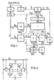
- FIG. 1 denotes a memory field which is constructed from a multiplicity of static memory cells, for example according to FIG. 2, in complementary circuit technology.
- each of these memory cells has two cross-coupled inverters, the first of which consists of the series connection of two field effect transistors T1 and T2, the second of the series connection of two field effect transistors T3 and T4.
- the source connections of the p-channel transistors T1 and T3 are connected to a connection 2 which is connected to a supply voltage V DD of, for example, 5 V.
- the source connections the n-channel transistors T2 and T4 are connected to a terminal 3 which is connected to the reference potential V SS .
- the drain connections of T1 and T2 are connected to one another in a node 4, the drain connections of the transistors T3 and T4 in a node 5.
- the interconnected gate connections of T1 and T2 are connected to the node 5 and the interconnected gate connections of T3 and T4 with node 4.
- Nodes 4 and 5 are each connected to data lines L and via the source-drain paths of n-channel selection transistors T5 and T6 L connected.
- the gates of T5 and T6 are controlled via a word line WL.
- the memory cells are combined in rows and columns in the memory array 1, in such a way that all the memory cells of a row are located on a common word line WL, while all of the memory cells of a column have a common data line pair L, L exhibit.
- the word lines of all lines of the memory array 1 are designated WL i in FIG. 1, the data line pairs L, L all columns with L i , L i .
- the data line pairs L i , L i are connected on the one hand to the inputs of a sense amplifier 6 and on the other hand to the outputs of a write-in circuit 7. Furthermore, they are connected to the outputs 8 of a precharge circuit 9, through which they can be supplied with a predetermined potential.
- the precharge circuit 9 contains, for example, n-channel transistors, the source connections of which represent the outputs 8, their drain connections being connected to the supply voltage V DD .
- the control connections of the n-channel transistors are connected to a control input 10.
- the outputs 11a, 11b of the sense amplifier 6 are connected to a data output DA via a buffer 12 and a buffer amplifier 13, while a data input DE is connected to an input 15 of the write-in circuit 7 via a buffer amplifier 14.
- a block 16 represents the row decoding, a block 17 the column decoding and the write / read control of the semiconductor memory.
- n-digit that is to say n-bit, address signal A
- n-bit that is to say n-bit, address signal A
- n inputs 16a of the row decoding 16 over n lines 18 and n buffer amplifier 19 connected to n inputs 20, and n inputs 17a of 17 via n lines 21 and the buffer amplifier 19 also to the inputs 20.
- the outputs of the row decoding 16 are connected to the word lines WL i , the outputs of the column decoding and writing / Read controller 17 via output lines 22 and 23 to the circuit units 6, 7, 12, 13 and 14.
- a further line 21 connects a further input 20, to which a read / write signal RW is present, to a further input 17a of FIG Finally, an input 20 is also provided, to which a chip select signal CS is fed and which is connected to additional inputs 16a and 17a via additional lines 18 and 21.
- a total of n + 2 inputs 20 are therefore provided, which are connected to the inputs of n + 2 identically constructed signal change detection circuits 24, the common output 25 of which is connected to a first input of a clock voltage generator 26.
- a second input 27 of the clock voltage generator 26 is connected to the output 28a of a control circuit 28, the inputs of which are at the outputs 11a and 11b of the sense amplifier 6.
- a first output 29 of 26 is connected to the control input 10 of the precharge circuit 9, while a second output 30 of 26 is connected via a line 31 to an input of the column decoding and read / write control 17 and additionally via a line 32 to an input 16b of the row decoding 16 can be connected.
- the output line 22 of FIG. 17 is also connected to another input of the control circuit 28.
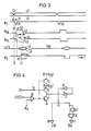
- the inputs 20 are supplied with a corresponding address signal A which differs from the previously applied address signal, so that an address signal change takes place.
- This is represented in FIG. 3 by the intersection 33 of two voltage profiles plotted over time t.
- the one voltage curve U1 can represent a bit of a first address signal which, at time t1, changes from an upper voltage value, for example a "1", to a lower voltage value, eg a "0" changes while the other voltage curve U2 illustrates a bit of a second address signal which changes from "0" to "1" at time t1.
- At least one of the signal change detection circuits 24 derives a pulse-shaped output signal 34 from the address signal change at time t1, the falling edge of which (transition from “1 to” 0 ") is delayed by a time period D1 compared to t1.
- the clock voltage generator specifies at its output 29 from the time t1 a first clock voltage ⁇ VL , which is fed to the control input 10 of the precharge circuit, ⁇ VL has a voltage level "1" which activates the precharge circuit 9, so that the data lines L i , L i are preloaded to a predetermined potential.
- the falling edge of the output signal 34 causes, after a delay time of D2, the first clock voltage ⁇ VL to be switched to a voltage level "0" and thus a deactivation of the precharge circuit 9, that is to say the disconnection of the data lines from a voltage source causing the precharge.
- a second clock voltage ⁇ DK which occurs at the output 30, is switched from a voltage level "0" to a voltage level "1", which activates the column decoding and read / write circuit 17 and, if an internal clocking of the row decoding is provided leads to an activation of 16.
- the desired memory cell is thus addressed and the memory can be accessed.
- the sense amplifier 6 and the circuit units 12 and 13 are activated, which is done by means of the read / write signal R / W, which is switched to a first voltage level, while the write circuit 7 and the buffer amplifier 14 remain deactivated.
- the row decoding 16 then does not need to be activated or deactivated by means of the clock voltage ⁇ DK if the individual memory cells are dimensioned such that the data lines connected to the voltage source used for precharging together with a selected word line do not falsify the stored signals in the can lead to memory cells located on the selected word line.
- the control circuit 28 evaluates the read signal LA occurring at the outputs 11a and 11b of the sense amplifier 6, LA out. It recognizes whether a certain signal amplitude is exceeded. If this is the case, the output signal ⁇ R of the control circuit 28 goes from “1" to "0". 3, this occurs at time t2.
- the clock voltage generator 26 is controlled via its input 27 such that the clock voltage ⁇ DK is first switched from “1" to "0” after a delay time D3 and the clock voltage ⁇ VL after a delay time D4 exceeding D3 is switched back from "0" to "1".
- the output signal LA, LA reaches the buffer 12 via the outputs 11a, 11b and is transferred via the output and the buffer amplifier 13 to the data output DA. At this it is then available until a new signal occurs at the outputs 11a, 11b, which in turn is transferred to the buffer memory 12.
- the supply of the address signal assigned to this memory cell causes an address signal change which again results in an output signal 34 and at a time interval from D2 from its falling edge for deactivating the precharge circuit by means of ⁇ VL and for activating the Blocks 16 and 17 by means of ⁇ DK leads.
- This memory cell is thus addressed.
- the signal R / W is switched to a second voltage level, which characterizes a write-in process, so that an output signal 34 of the circuit 24 is generated even when the address signals A are not changed.
- Blocks 6, 7 and 14 are activated by the second voltage level of R / W, while 12 and 13 remain deactivated.
- the signal to be written now arrives via 14, 15 and 7 on the selected data line pair L, L and to the inputs of the sense amplifier 6, which leads to the output of an output signal LA, LA leads to the outputs 11a and 11b.
- the control circuit 28 evaluates this output signal again in that ⁇ R goes from “1” to “0".
- the falling edge 60 controls the clock voltage generator 26 such that ⁇ DK is switched back from “1” to “0” and ⁇ VL from "0" to "1".
- ⁇ R is switched from "0" to "1"
- the clock voltage generator 26 can again recognize a new signal 34 'of the circuit 24.
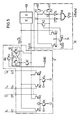
- the output signal 34 of the signal change detection circuit is here fed to the gate of a p-channel transistor P1, the source of which is connected to the supply voltage V DD via a connection 35 and the drain of which is connected to an internal node K1.
- the output signal ⁇ R of the control circuit 28 is applied to a first input of a NAND gate 36, the output of which is connected to the gate of an n-channel transistor N1.
- the source and drain of N1 are connected to the reference potential V SS and to the internal node K1.
- a second entrance 37 of gate 36 is expediently assigned a signal CS, which is referred to as a "chip select" signal.
- a holding circuit consisting of inverters I1 and I2 is connected to node K1.
- K1 is connected via a buffer amplifier 38 to the output 30, at which the clock voltage ⁇ DK is available.
- K1 is connected directly to the first input of a NOR gate 39 and via a delay circuit 40, for example an inverter chain, to a second input of 39.
- the output of 39 is led via a buffer amplifier 41 to the output 29, at which the clock voltage ⁇ VL is tapped.
- the circuit parts 39 and 40 provide a delay of the rising edge 42 of ⁇ VL compared to the falling edge 43 of ⁇ DK , which is necessary to ensure that the decoding of the memory is switched off before the precharge circuit 9 is switched on.
- the state of the node K1 can be set to "0" or "1” via the transistors N1 and P1.
- the falling edge of output signal 34 sets node K1 to "1” by switching P1 on. This state is then no longer changed by further output signals 34.
- ⁇ VL is set to "0” and ⁇ DK to "1”
- N1 has a substantially smaller resistance between its source and its drain connection than the transistor P1 in the conductive state.
- N1 and P1 must be dimensioned so that they deliver significantly more current than the inverter I2.
- connection 35 is expediently connected via a p-channel transistor P2 to a connection 35 'which is connected to the supply voltage V DD instead of 35.
- the gate of P2 is then connected to the output of NAND gate 36.
- P2 serves as a switching transistor which switches off the supply voltage V DD from the terminal 35 when the transistor N1 is switched on. This prevents the occurrence of a cross flow.
- Fig. 5 shows a preferred embodiment of the control circuit 28 and an appropriate circuit design of the sense amplifier 6.
- the sense amplifier 6 has 2n data line inputs, of which the first two designated E1 and E1 'and with the data lines L1 and L 1 the first column of the memory field 1 are connected.
- the drain of N21 is connected to the output 11a, the drain of N11 to the output 11b.
- the gate of N11 is connected to the input E1, the gate of N21 with the input E1 '.
- the node 42a is connected to the drain connection of the base transistor N31, the source of which is connected to reference potential via a connection 43a.
- the gate of N3 1 is connected via a connection 44 to a first output of the column decoding 17, to which a "1" is present when the data line pair L 1, L 1 is selected.
- the further data line inputs of the sense amplifier 6 are assigned in an analog manner to n-channel transistors which are connected in a corresponding manner to 11a and 11b, the gate connections of the base transistors being in each case at the other outputs of the column decoding 17.
- the inputs E n and E n 'assigned n-channel transistors are designated N1 n , N2 n and N3 n .
- the gate connection of the base transistor N3 n has the reference numeral 45, while 46 denotes the source terminal of N3 n , which is at reference potential.
- the output 11b is connected to the drain connection of a p-channel transistor PL1, the source connection of which lies at a node 47.
- the output 11a is connected to the drain connection of a p-channel transistor PL2, the source connection of which is connected to the node 47.
- the gate connection of PL1 is connected to the drain connection of PL2, the gate connection PL2 is connected to the drain connection of PL1.
- the node 47 is led via the source-drain path of a further p-channel transistor PS1 to a connection 48 which is connected to the supply voltage V DD .
- the outputs 11a and 11b are connected to one another via the source-drain path of an n-channel field-effect transistor N2, the gates of PS1 and N2 being connected to a connection 49.
- the transistors PL1 and PL2 represent a p-channel load part 50 of the sense amplifier 6.
- a buffer 12 and a buffer amplifier 13 are connected to the outputs 11a and 11b, the output of which represents the data output DA.
- the embodiment of the control circuit 28 shown in FIG. 5 contains three n-channel transistors NE1, NE2 and NE3, the first two of which are connected with their source connections to a node 51, the drain connection of NE1 at a node 52 and the drain connection of NE2 lie at a node 53.
- the gate of NE1 is connected to output 11a, the gate of NE2 is connected to output 11b.
- the node 51 is connected via the source-drain path of NE3 to a connection 54 which is at reference potential V SS .
- the gate connection of NE3 is designated 55.
- the node 52 is connected via the source-drain path of a p-channel transistor PE1 to a terminal 56 which is connected to the supply voltage V DD .
- the node 53 is connected via the source-drain path of a p-channel transistor PE2 to a connection 57, to which the supply voltage is likewise fed.
- the gate of PE1 is connected to the drain connection of PE2 and the gate of PE2 is connected to the drain connection of PE1.
- Nodes 52 and 53 are across the source-drain path a p-channel transistor PE3 connected to one another, the gate of which is connected to the terminal 55.
- the nodes 52 and 53 are led via inverters I3 and I4 to the inputs of a NOR gate 58, the output of which is connected to the output 28a via a buffer amplifier 59.
- the base transistor that belongs to the selected column is turned on.
- the signal present at connection 49 is switched from “1" to "0".
- the outputs 11a and 11b are decoupled from one another, the supply voltage V DD being applied to the node 47 through the switching on of PS1.
- the signal present at the gate terminal 55 which is inverted to the signal present at 49, is switched from "0" to "1”.
- the transistor NE3 is thus turned on, while the transistor PE3 blocks. Since the potentials on the selected data lines change in opposite directions depending on the signal to be read out, this is also the case at the outputs 11a and 11b of the sense amplifier 6 representing a differential amplifier. The opposing potential changes occurring there are shown in FIG.
- LA and LA designated.
- LA or LA changes in the direction of the reference potential and a corresponding potential change also occurs at node 52 or 53, the This means that the response threshold of one of the inverters I3 or I4 is not reached.
- the relevant inverter thus recognizes an input signal “0” and applies a "1" to the downstream input of the NOR gate 58.
- the signal ⁇ R occurring at the output 28a is switched from “1” to "0".
- This changeover which is indicated in FIG. 3 by the falling edge 60 of ⁇ R , has the effect that after the delay time D3 has elapsed, the transistor N1 is turned on, so that the node K1 (FIG.
- the load part 50 of the sense amplifier 6 can also be designed such that the gates of PL1 and PL2 are connected to one another and connected to the drain connection of PL1.
- the gates of PL1 and PL2 can also be connected to one another and led to a reference voltage connection. In this case, however, is that in the previous paragraph Simplification of the control circuit 28 described is not permitted.
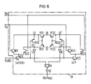
- FIG. 6 shows a further embodiment of the control circuit 28, in which a bistable circuit design, as is given by the cross-coupled transistors PE1 and PE2 in FIG. 5, is avoided.
- a first differential amplifier circuit which largely corresponds in structure to that shown in FIG. 5, is shown in the left part of FIG. 6.
- the n-channel transistors NE11 to NE13 and the p-channel transistors PE11 to PE13 correspond to the circuit parts NE1 to NE3 and PE1 to PE3 in FIG. 5, the difference being that the gate connections of PE11 and PE12 correspond to the Drain connection of PE11 are connected.
- node 53 is connected to an inverter input, but node 52 is no longer tapped via an inverter input.
- a second differential amplifier circuit which corresponds completely to the first in construction, forms the right part of the circuit according to FIG. 6. It contains n-channel transistors NE21 to NE23 and p-channel transistors PE21 to PE23 in a part on the left part of FIG. 6 corresponding circuit configuration.
- the gate connection of NE21 is connected to the output 11a, the gate connection of NE22 to the output 11b.
- the source connection of NE23 lying at reference potential V SS is designated 54 '.
- the drain connections of PE21 and PE22 are labeled 52 'and 53'. Again, only node 53 'is connected to an inverter input, node 52' is not.
- inverters I5 and I6 which correspond to inverters I3 and I4 of FIG. 5, are connected to nodes 53 and 53 'according to FIG. 6.
- the outputs of I5 and I6 are at the inputs of a NOR gate 61, the output of which is connected to the output 28a via a buffer amplifier 62.
- the nodes 52 and 53 and 52 'and 53' are precharged to a potential V DD -V t , where V t again means the threshold voltage of the transistors PE11 or PE12 or PE21 or PE22.
- V t again means the threshold voltage of the transistors PE11 or PE12 or PE21 or PE22.
- disturbances or production-related asymmetries between the transistors NE1 and NE2 or PE1 and PE2 can lead to the circuit adopting one of its two stable states without a signal swing occurring at the circuit points 11a and 11b.
- this danger only exists if the transistor PE3 is blocked for a long time before a signal swing occurs at 11a and 11b. 6, this danger is completely eliminated.
- a signal change detection circuit 24 is, for example, from IEEE journals. of Solid-State Circuits, Vol. SC-19, Oct. 1984, pp. 545-551.
- an output signal 34 circuits 24 constructed simultaneously connect each of the n + 2 inputs 20.
- the inputs E i , E i ' can also be connected to the outputs of an upstream amplifier stage instead of the data lines L i , ⁇ L i , which in turn are connected to the data lines mentioned is connected.
- the sense amplifier 6 shown in Fig. 5 can be simplified insofar as only one n-channel transistor circuit, for example that provided with the transistors N11 to N31, provided that the selection of the desired data line pair before the input, for example E1 and E1 ', The remaining single-stage sense amplifier is made, for example, in the upstream amplifier stages.
- the switching thresholds of the inverters I3 to I6 can be set in a manner known per se by the ratio of the channel widths of the p- and n-channel transistors contained in them to a relatively low value of, for example, 1.5 V when the supply voltage V DD is approximately Is 5 V. This ensures that the precharge potential at nodes 52, 53 and 53 ', which is lower than V DD by the threshold voltage V t, is still reliably recognized by the inverters as an input signal "1".
- a gate circuit 19a can be provided, which is controlled by means of ⁇ DK in such a way that it blocks during a memory access. This prevents further address signals from reaching decoders 16 and 17 during memory access.
- the word width of the memory is greater than 1 bit.
- m memory fields 1, precharge circuits 9, sense amplifiers 6, write circuits 7, intermediate memories 12, buffer amplifiers 13, 14 and data outputs and inputs DA, DE are provided.
- the outputs of blocks 16 and 17 are then each with m corresponding word and data lines or sense amplifiers, write circuits, intermediate memories and Buffer amplifiers connected.
- the control circuit 28 is expediently only connected to the outputs 11a and 11b of one of the m sense amplifiers.
Landscapes
- Engineering & Computer Science (AREA)
- Microelectronics & Electronic Packaging (AREA)
- Computer Hardware Design (AREA)
- Static Random-Access Memory (AREA)
- Read Only Memory (AREA)
- Oscillators With Electromechanical Resonators (AREA)
Abstract
Description
Die Erfindung bezieht sich auf einen Halbleiterspeicher mit einer Signalwechsel-Erkennungsschaltung nach dem Oberbegriff des Patentanspruchs 1.The invention relates to a semiconductor memory with a signal change detection circuit according to the preamble of
Ein Halbleiterspeicher dieser Art ist aus der EP-A-0 107 415 bekannt. Dort wird in der Signalwechsel-Erkennungsschaltung aus jedem Adreßsignalwechsel ein Ausgangssignal abgeleitet, das zunächst einem ersten Steuereingang der Vorladeschaltung zugeführt wird, an dem es eine Deaktivierung derselben veranlaßt. Andererseits wird das Ausgangssignal über eine Verzögerungseinheit einem zweiten Steuereingang der Vorladeschaltung zugeführt, an dem es eine Reaktivierung derselben bewirkt. Die Verzögerungseinheit verzögert das Ausgangssignal dabei um eine feste Zeitspanne, die für den zeitaufwendigsten Speicherzugriff vorgesehen werden muß.A semiconductor memory of this type is known from EP-A-0 107 415. There, an output signal is derived in the signal change detection circuit from each address signal change, which is first fed to a first control input of the precharge circuit, at which it causes the same to be deactivated. On the other hand, the output signal is fed via a delay unit to a second control input of the precharge circuit, at which it causes the same to be reactivated. The delay unit delays the output signal by a fixed period of time, which must be provided for the most time-consuming memory access.
Der Erfindung liegt die Aufgabe zugrunde, einen Halbleiterspeicher der eingangs genannten Art anzugeben, bei dem eine aus Signalwechseln abgeleitete Taktung der Vorladeschaltung wesentlich besser auf die tatsächliche Dauer der einzelnen Speicherzugriffe abgestimmt werden kann, als das bei dem vorstehend erwähnten, bekannten Halbleiterspeicher der Fall ist. Das wird erfindungsgemäß durch eine Ausbildung nach dem Kennzeichen des Patentanspruchs 1 erreicht.The invention has for its object to provide a semiconductor memory of the type mentioned, in which a timing of the precharge circuit derived from signal changes can be matched to the actual duration of the individual memory accesses much better than is the case with the known semiconductor memory mentioned above. This is achieved according to the invention by training according to the characterizing part of
Der mit der Erfindung erzielbare Vorteil liegt insbesondere darin, daß die Reaktivierung der Vorladeschaltung baldmöglichst nach der Beendigung jedes einzelnen Speicherzugriffs erfolgen kann, so daß der Speicher in jeweils kürzester Zeit für einen neuen Zugriff wieder zur Verfügung steht. Ein weiterer Vorteil besteht darin, daß die extrem schnelle Reaktivierung der Vorladeschaltung auch unabhängig von der Anzahl der Speicherzellen im Speicherfeld und damit unabhängig von der hierdurch bedingten unterschiedlichen Dauer der Speicherzugriffe gewährleistet ist.The advantage that can be achieved with the invention is, in particular, that the precharge circuit can be reactivated as soon as possible after the end of each individual memory access, so that the memory is available for a new access in the shortest possible time. Another advantage is that the extremely fast reactivation of the precharge circuit independent of the number of memory cells in the memory field and thus independent of the resulting different duration of memory access.
Bevorzugte Ausgestaltungen und Weiterbildungen der Erfindung sind in den Patentansprüchen 2 bis 13 angegeben.Preferred refinements and developments of the invention are specified in claims 2 to 13.
Die Erfindung wird nachfolgend anhand der in der Zeichnung dargestellten, bevorzugten Ausführungsbeispiele näher erläutert. Dabei zeigt:
- Fig. 1
- das Blockschaltbild eines erfindungsgemäßen Halbleiterspeichers,
- Fig. 2
- die Prinzipschaltung einer Speicherzelle des Speichers nach Fig. 1,
- Fig. 3
- Spannungs-Zeit-Diagramme zur Erläuterung der Wirkungsweise des Speichers nach Fig. 1,
- Fig. 4
- das Prinzipschaltbild einer Teilschaltung von Fig. 1,
- Fig. 5
- das Prinzipschaltbild einer anderen Teilschaltung von Fig. 1 und
- Fig. 6
- eine alternative Ausbildung der Teilschaltung nach Fig. 5.
- Fig. 1
- the block diagram of a semiconductor memory according to the invention,
- Fig. 2
- the basic circuit of a memory cell of the memory of FIG. 1,
- Fig. 3
- Voltage-time diagrams to explain the mode of operation of the memory according to FIG. 1,
- Fig. 4
- the basic circuit diagram of a partial circuit of Fig. 1,
- Fig. 5
- the schematic diagram of another subcircuit of Fig. 1 and
- Fig. 6
- an alternative embodiment of the subcircuit according to FIG. 5.
In Fig. 1 bezeichnet 1 ein Speicherfeld, das aus einer Vielzahl von z.B. nach Fig. 2 ausgebildeten, statischen Speicherzellen in komplementärer Schaltungstechnik aufgebaut ist. Jede dieser Speicherzellen weist gemäß Fig. 2 zwei kreuzgekoppelte Inverter auf, von denen der erste aus der Serienschaltung zweier Feldeffekttransistoren T1 und T2 besteht, der zweite aus der Serienschaltung zweier Feldeffekttransistoren T3 und T4. Die Sourceanschlüsse der p-Kanal-Transistoren T1 und T3 sind mit einem Anschluß 2 verbunden, der mit einer Versorgungsspannung VDD von z.B. 5 V beschaltet ist. Die Sourceanschlüsse der n-Kanal-Transistoren T2 und T4 liegen an einem Anschluß 3, der mit dem Bezugspotential VSS beschaltet ist. Die Drainanschlüsse von T1 und T2 sind in einem Knoten 4 miteinander verbunden, die Drainanschlüsse der Transistoren T3 und T4 in einem Knoten 5. Zur Realisierung der Kreuzkopplung sind die miteinander verbundenen Gateanschlüsse von T1 und T2 mit dem Knoten 5 verbunden und die miteinander verbundenen Gateanschlüsse von T3 und T4 mit dem Knoten 4. Die Knoten 4 und 5 sind jeweils über die Source-Drain-Strecken von n-Kanal-Auswahltransistoren T5 und T6 mit Datenleitungen L und
Die Speicherzellen sind im Speicherfeld 1 zeilen- und spaltenweise zusammengefaßt, und zwar derart, daß sämtliche Speicherzellen einer Zeile an einer gemeinsamen Wortleitung WL liegen, während sämtliche Speicherzellen einer Spalte ein gemeinsames Datenleitungspaar L,
Bei einem n-stelligen, das heißt n Bit umfassenden Adreßsignal A sind n Eingänge 16a der Zeilendecodierung 16 über n Leitungen 18 und n Pufferverstärker 19 mit n Eingängen 20 verbunden, sowie n Eingänge 17a von 17 über n Leitungen 21 und die Pufferverstärker 19 ebenfalls mit den Eingängen 20. Die Ausgänge der Zeilendecodierung 16 sind mit den Wortleitungen WLi beschaltet, die Ausgänge der Spaltendecodierung und Schreib/ Lese-Steuerung 17 über Ausgangsleitungen 22 und 23 mit den Schaltungseinheiten 6, 7, 12, 13 und 14. Eine weitere Leitung 21 verbindet einen weiteren Eingang 20, an dem ein Schreib-/Lesesignal RW anliegt, mit einem weiteren Eingang 17a von 17. Schließlich ist noch ein Eingang 20 vorgesehen, dem ein Chip-Select-Signal CS zugeführt wird und der über zusätzliche Leitungen 18 und 21 mit zusätzlichen Eingängen 16a und 17a verbunden ist.In the case of an n-digit, that is to say n-bit, address signal A, there are n
Insgesamt sind also n + 2 Eingänge 20 vorgesehen, die mit den Eingängen von n + 2 gleichartig aufgebauten Signalwechsel-Erkennungsschaltungen 24 verbunden sind, deren gemeinsamer Ausgang 25 mit einem ersten Eingang eines Taktspannungsgenerators 26 beschaltet ist. Ein zweiter Eingang 27 des Taktspannungsgenerators 26 ist mit dem Ausgang 28a einer Steuerschaltung 28 verbunden, deren Eingänge an den Ausgängen 11a und 11b des Leseverstärkers 6 liegen. Ein erster Ausgang 29 von 26 ist mit dem Steuereingang 10 der Vorladeschaltung 9 beschaltet, während ein zweiter Ausgang 30 von 26 über eine Leitung 31 mit einem Eingang der Spaltendecodierung und Schreib/Lese-Steuerung 17 verbunden ist und zusätzlich über eine Leitung 32 mit einem Eingang 16b der Zeilendecodierung 16 verbunden sein kann. Die Ausgangsleitung 22 von 17 ist auch mit einem weiteren Eingang der Steuerschaltung 28 verbunden.A total of n + 2 inputs 20 are therefore provided, which are connected to the inputs of n + 2 identically constructed signal
Beim Adressieren einer Speicherzelle, z.B. T1 bis T6, zum Zweck des Auslesens eines in dieser gespeicherten Signals über DA, wird den Eingängen 20 ein entsprechendes Adreßsignal A zugeführt, das sich von dem vorher anliegenden Adreßsignal unterscheidet, so daß ein Adreßsignalwechsel erfolgt. Dieser wird in Fig. 3 durch den Schnittpunkt 33 zweier über der Zeit t aufgetragener Spannungsverläufe dargestellt. Der eine Spannungsverlauf U1 kann dabei ein Bit eines ersten Adreßsignals darstellen, das zum Zeitpunkt t1 von einem oberen Spannungswert, zum Beispiel einer "1", auf einen unteren Spannungswert, Z.B. eine "0", übergeht, während der andere Spannungsverlauf U2 ein Bit eines zweiten Adreßsignals veranschaulicht, das zum Zeitpunkt t1 von "0" auf "1" geht.When addressing a memory cell, for example T1 to T6, for the purpose of reading out a signal stored in it via DA, the inputs 20 are supplied with a corresponding address signal A which differs from the previously applied address signal, so that an address signal change takes place. This is represented in FIG. 3 by the
Wenigstens eine der Signalwechsel-Erkennungsschaltungen 24 leitet aus dem Adreßsignalwechsel zum Zeitpunkt t1 ein impulsförmiges Ausgangssignal 34 ab, dessen fallende Flanke (Übergang von "1 auf "0") um eine Zeitspanne D1 gegenüber t1 verzögert ist. Der Taktspannungsgenerator gibt an seinem Ausgang 29 vor dem Zeitpunkt t1 eine erste Taktspannung ØVL ab, die dem Steuereingang 10 der Vorladeschaltung zugeführt wird. ØVL weist dabei einen Spannungspegel "1" auf, der die Vorladeschaltung 9 aktiviert, so daß die Datenleitungen Li,
Die Steuerschaltung 28 wertet das an den Ausgängen 11a und 11b des Leseverstärkers 6 auftretende, gelesene Signal LA,
Unter der Annahme, daß in der adressierten Speicherzelle T1 bis T6 vor dem Zeitpunkt t1 eine "1" gespeichert war, wobei der Knoten 4 zum Beispiel mit der Versorgungsspannung VDD belegt ist und der Knoten 5 auf Bezugspotential liegt, und unter der weiteren Annahme, daß die Datenleitungen L und
Das Ausgangssignal LA,
Soll in eine Speicherzelle ein Signal eingeschrieben werden, so bewirkt die Zuführung des dieser Speicherzelle zugeordneten Adreßsignals einen Adreßsignalwechsel, der wieder zu einem Ausgangssignal 34 und im zeitlichen Abstand von D2 von dessen fallender Flanke zu einer Deaktivierung der Vorladeschaltung mittels ØVL sowie zu einer Aktivierung der Blöcke 16 und 17 mittels ØDK führt. Damit ist diese Speicherzelle adressiert. Weiterhin wird das Signal R/W auf einen zweiten Spannungspegel umgeschaltet, der einen Einschreibvorgang kennzeichnet, so daß auch bei nicht geänderten Adreßsignalen A ein Ausgangssignal 34 der Schaltung 24 erzeugt wird. Durch den zweiten Spannungspegel von R/W werden die Blöcke 6, 7 und 14 aktiviert, während 12 und 13 deaktiviert bleiben. Das einzuschreibende Signal gelangt nun über 14, 15 und 7 auf das selektierte Datenleitungspaar L,
Fig. 4 zeigt ein Beispiel eines Taktspannungsgenerators 26 in komplementärer Schaltungstechnik. Das Ausgangssignal 34 der Signalwechsel-Erkennungsschaltung wird hier auf das Gate eines p-Kanal-Transistors P1 geführt, dessen Source über einen Anschluß 35 mit der Versorgungsspannung VDD belegt ist und dessen Drain mit einem internen Knoten K1 verbunden ist. Das Ausgangssignal ØR der Steuerschaltung 28 ist auf einen ersten Eingang eines NAND-Gatters 36 gelegt, dessen Ausgang mit dem Gate eines n-Kanal-Transistors N1 verbunden ist. Source und Drain von N1 sind an das Bezugspotential VSS bzw. an den internen Knoten K1 angeschlossen. Ein zweiter Eingang 37 des Gates 36 ist zweckmäßigerweise mit einem Signal CS belegt, das als "Chip select"-Signal bezeichnet wird. Nimmt CS den Wert "1" an, so ist der Halbleiterspeicher als solcher aktiviert, während ein Wert "0" die Unwirksamschaltung des Speichers bedeutet. Eine aus den Invertern I1 und I2 bestehende Halteschaltung ist mit dem Knoten K1 verbunden. K1 ist über einen Pufferverstärker 38 mit dem Ausgang 30 beschaltet, an dem die Taktspannung ØDK zur Verfügung steht. Weiterhin ist K1 direkt mit dem ersten Eingang eines NOR-Gatters 39 und über eine Verzögerungsschaltung 40, z.B. eine Inverterkette, mit einem zweiten Eingang von 39 verbunden. Der Ausgang von 39 ist über einen Pufferverstärker 41 an den Ausgang 29 geführt, an dem die Taktspannung ØVL abgegriffen wird. Durch die Schaltungsteile 39 und 40 erhält man eine Verzögerung der ansteigenden Flanke 42 von ØVL gegenüber der abfallende Flanke 43 von ØDK, die erforderlich ist, um sicherzustellen, daß die Decodierung des Speichers abgeschaltet ist, bevor die Vorladeschaltung 9 eingeschaltet wird.4 shows an example of a
Der Zustand des Knotens K1 läßt sich über die Transistoren N1 und P1 auf "0" oder "1" setzen. Dabei setzt die fallende Flanke des Ausgangssignals 34 durch Leitendschaltung von P1 den Knoten K1 auf "1". Durch weitere Ausgangssignale 34 wird dieser Zustand dann nicht mehr geändert. Mit dem auf "1" gesetzten Knoten K1 werden ØVL auf "0" und ØDK auf "1" gesetzt, so daß die Vorladeschaltung 9 deaktiviert und die Decodierungen 16, 17 aktiviert werden. Andererseits bewirken die Zustände ØR = 0 (Steuerschaltung erkennt ein Ausgangssignal LA,
Mit CS = "0" oder ØR = "0" muß K1 auch bei gleichzeitig eingeschaltetem Transistor T1 sicher in den logischen Zustand "0" gebracht werden. Dies setzt voraus, daß N1 im leitenden Zustand einen wesentlichen kleineren Widerstand zwischen seinem Source- und seinem Drainanschluß aufweist, als der Transistor P1. Weiterhin sind N1 und P1 so zu dimensionieren, daß sie deutlich mehr Strom liefern als der Inverter I2.With CS = "0" or Ø R = "0", K1 must be safely brought into the logic state "0" even when transistor T1 is switched on at the same time. This presupposes that N1 has a substantially smaller resistance between its source and its drain connection than the transistor P1 in the conductive state. Furthermore, N1 and P1 must be dimensioned so that they deliver significantly more current than the inverter I2.
In der Schaltung nach Figur 4 tritt bei gleichzeitig leitenden Transistoren P1 und N1 ein Querstrom und damit eine unverwünschte Verlustleistung auf. Um das zu vermeiden, wird zweckmäßigerweise der Anschluß 35 über einen p-Kanal-Transistor P2 mit einem Anschluß 35′ verbunden, der anstelle von 35 mit der Versorgungsspannung VDD beschaltet ist. Das Gate von P2 ist dann mit dem Ausgang des NAND-Gatters 36 verbunden. P2 dient als Schalttransistor, der bei leitend geschaltetem Transistor N1 die Versorgungsspannung VDD vom Anschluß 35 abschaltet. Damit wird das Auftreten eines Querstromes verhindert.In the circuit according to FIG. 4, with transistors P1 and N1 conducting at the same time, a cross current occurs and thus an undesired power loss. To avoid this, the
Fig. 5 zeigt eine bevorzugte Ausführungsform der Steuerschaltung 28 und eine zweckmäßige schaltungstechnische Durchbildung des Leseverstärkers 6. Der Leseverstärker 6 weist dabei 2n Datenleitungseingänge auf, von denen die ersten beiden mit E1 und E1′ bezeichnet und mit den Datenleitungen L₁ und
Der Ausgang 11b ist mit dem Drainanschluß eines p-Kanal-Transistors PL1 verbunden, dessen Sourceanschluß an einem Knoten 47 liegt. Analog hierzu ist der Ausgang 11a mit dem Drainanschluß eines p-Kanal-Transistors PL2 beschaltet, dessen Sourceanschluß mit dem Knoten 47 verbunden ist. Der Gateanschluß von PL1 ist mit dem Drainanschluß von PL2 beschaltet, der Gateanschluß PL2 von mit dem Drainanschluß von PL1. Der Knoten 47 ist über die Source-Drain-Strecke eines weiteren p-Kanal-Transistors PS1 an einen Anschluß 48 geführt, der mit der Versorgungsspannung VDD beschaltet ist. Weiterhin sind die Ausgänge 11a und 11b über die Source-Drain-Strecke eines n-Kanal-Feldeffekttransistors N2 miteinander verbunden, wobei die Gates von PS1 und N2 an einen Anschluß 49 gelegt sind. Die Transistoren PL1 und PL2 stellen einen p-Kanal-Lastteil 50 des Leseverstärkers 6 dar. An den Ausgängen 11a und 11b sind gemäß Figur 1 ein Zwischenspeicher 12 und ein Pufferverstärker 13 angeschlossen, dessen Ausgang den Datenausgang DA darstellt.The
Die in Fig. 5 gezeigte Ausführungsform der Steuerschaltung 28 enthält drei n-Kanal-Transistoren NE1, NE2 und NE3, von denen die beiden ersten mit ihren Sourceanschlüssen an einen Knoten 51 gelegt sind, wobei der Drainanschluß von NE1 an einem Knoten 52 und der Drainanschluß von NE2 an einem Knoten 53 liegen. Der Gateanschluß von NE1 ist mit dem Ausgang 11a verbunden, der Gateanschluß von NE2 mit dem Ausgang 11b. Der Knoten 51 ist über die Source-Drain-Strecke von NE3 mit einem Anschluß 54 verbunden, der auf Bezugspotential VSS liegt. Der Gateanschluß von NE3 ist mit 55 bezeichnet. Der Knoten 52 ist über die Source-Drain-Strecke eines p-Kanal-Transistors PE1 mit einem Anschluß 56 verbunden, der mit der Versorgungsspannung VDD beschaltet ist. Analog hierzu ist der Knoten 53 über die Source-Drain-Strecke eines p-Kanal-Transistors PE2 mit einem Anschluß 57 verbunden, dem ebenfalls die Versorgungsspannung zugeführt wird. Dabei sind das Gate von von PE1 mit dem Drainanschluß von PE2 verbunden und das Gate von PE2 mit dem Drainanschluß von PE1. Die Knoten 52 und 53 sind über die Source-Drain-Strecke eines p-Kanal-Transistors PE3 miteinander verbunden, dessen Gate an den Anschluß 55 gelegt ist. Weiterhin sind die Knoten 52 und 53 über Inverter I3 bzw. I4 an die Eingänge eines NOR-Gatters 58 geführt, dessen Ausgang über einen Pufferverstärker 59 mit dem Ausgang 28a in Verbindung steht.The embodiment of the
In der Vorladephase, d.h. mit ØVL = "1" und ØDK = "0", sind alle Fußpunkttransistoren N3₁ bis N3n des Leseverstärkers 6 gesperrt. Der Anschluß 49 ist mit einer "1" belegt, so daß die Ausgänge 11a und 11b über den Transistor N2 kurzgeschlossen sind und die Versorgungsspannung VDD über den gesperrten Transistor PS1 abgeschaltet ist. Der Gateanschluß 55 von NE3 ist mit einer "0" belegt, so daß NE3 sperrt und PE3 leitet. Damit liegen die Knoten 52 und 53 jeweils auf dem Potential VDD-Vt, wobei Vt die Einsatzspannung von PE1 bzw. PE2 bedeutet. Die Inverter I3 und I4 bewerten das Potential an 52 bzw. 53 jeweils als "1", so daß das an 28a abgreifbare Ausgangssignal ØR ebenfalls "1" ist.In the precharge phase, ie with Ø VL = "1" and Ø DK = "0", all
Beim Adressieren einer Speicherzelle wird derjenige Fußpunkttransistor, der zu der selektierten Spalte gehört, leitend geschaltet. Dabei wird das am Anschluß 49 anliegende Signal von "1" auf "0" umgeschaltet. Hierdurch werden die Ausgänge 11a und 11b voneinander entkoppelt, wobei durch die Leitendschaltung von PS1 die Versorgungsspannung VDD an den Knoten 47 angelegt wird. Weiterhin wird das am Gateanschluß 55 anliegende Signal, das zu dem bei 49 anliegenden Signal invertiert ist, von "0" auf "1" umgeschaltet. Damit wird der Transistor NE3 leitend geschaltet, während der Transistor PE3 sperrt. Da sich die Potentiale auf den selektierten Datenleitungen in Abhängigkeit von dem auszulesenden Signal in jeweils entgegengesetzter Richtung ändern, ist das auch an den Ausgängen 11a und 11b des einen Differenzverstärker darstellenden Leseverstärkers 6 der Fall. Die dort auftretenden gegenläufigen Potentialänderungen sind in Fig. 3 als LA und
Der Lasttteil 50 des Leseverstärkers 6 kann in Abweichung von Fig. 5 auch so ausgebildet sein, daß die Gates von PL1 und PL2 miteinander verbunden und an den Drainanschluß von PL1 gelegt sind. Andererseits können die Gates von PL1 und PL2 auch miteinander verbunden und an einen Referenzspannungsanschluß geführt sein. In diesem Fall ist jedoch die im vorstehenden Absatz beschriebene Vereinfachung der Steuerschaltung 28 nicht zulässig.5, the load part 50 of the
Fig. 6 zeigt eine weitere Ausführung der Steuerschaltung 28, bei der eine bistabile Schaltungsauslegung, wie sie durch die kreuzgekoppelten Transistoren PE1 und PE2 in Fig. 5 gegeben ist, vermieden wird. Eine erste Differenzverstärkerschaltung, die im Aufbau der in Fig. 5 dargestellten weitgehend entspricht, ist im linken Teil von Fig. 6 dargestellt. Dabei entsprechen die n-Kanal-Transistoren NE11 bis NE13 und die p-Kanal-Transistoren PE11 bis PE13 den Schaltungsteilen NE1 bis NE3 und PE1 bis PE3 in Fig. 5, wobei der Unterschied vorhanden ist, daß die Gateanschlüsse von PE11 und PE12 mit dem Drainanschluß von PE11 verbunden sind. Ein weiterer Unterschied besteht darin, daß der Knoten 53 mit einem Invertereingang verbunden ist, der Knoten 52 jedoch nicht mehr über einen Invertereingang abgegriffen wird. Eine zweite Differenzverstärkerschaltung, die der ersten im Aufbau vollständig entspricht, bildet den rechten Teil der Schaltung nach Fig. 6. Sie enthält n-Kanal-Transistoren NE21 bis NE23 und p-Kanal-Transistoren PE21 bis PE23 in einer dem linken Teil von Fig. 6 entsprechenden Schaltungskonfiguration. Der Gateanschluß von NE21 ist mit dem Ausgang 11a verbunden, der Gateanschluß von NE22 mit dem Ausgang 11b. Weiterhin ist der auf Bezugspotential VSS liegende Sourceanschluß von NE23 mit 54′ bezeichnet. Die Drainanschlüsse von PE21 und PE22 sind mit 52′ und 53′ bezeichnet. Auch hier ist nur der Knoten 53′ mit einem Invertereingang beschaltet, der Knoten 52′ dagegen nicht. Die Eingänge zweier Inverter I5 und I6, die den Invertern I3 und I4 von Fig. 5 entsprechen, sind nach Fig. 6 mit den Knoten 53 und 53′ verbunden. Die Ausgänge von I5 und I6 liegen an den Eingängen eines NOR-Gatters 61, dessen Ausgang über einen Pufferverstärker 62 an den Ausgang 28a gelegt ist.FIG. 6 shows a further embodiment of the
Nach Fig. 6 erfolgt eine Vorladung der Knoten 52 und 53 sowie 52′ und 53′ auf ein Potential VDD-Vt, wobei Vt wieder die Einsatzsspannung der Transistoren PE11 oder PE12 bzw. PE21 oder PE22 bedeutet. Beim Auslesen einer Speicherzelle sinkt das Potential in Abhängigkeit von dem gespeicherten Signal entweder am Ausgang 11a oder 11b des Leseverstärkers und dementsprechend auch am Knoten 53 oder 53′, wobei entweder I5 oder I6 die Potentialverringerung als ein Eingangssignal "0" erkennt und dem nachgeordneten Eingang des NOR-Gatters 61 eine "1" zuführt, was zur Umschaltung des Signals ØR am Ausgang 28 von "1" auf "0" führt. Beim Anlegen einer "1" an den Anschluß 55 werden die Potentiale an den Knoten 53 und 53′ über die leitenden Transistoren PE13 und PE23 wieder auf den Vorladewert VDD-Vt gebracht, so daß ØR auf den Wert "1" umgeschaltet wird.6, the
Die Anschlüsse 49 und 55 des Leseverstärkers 6 bzw. der Steuerschaltung 28 in Fig. 5 und Fig. 6 sind mit Signalen AG bzw.
Bei einer Ausführungsform der Steuerschaltung nach Figur 5 können Störungen oder fertigungsbedingte Unsymmetrien zwischen den Transistoren NE1 und NE2 oder PE1 und PE2 dazu führen, daß die Schaltung einen ihrer beiden stabilen Zustände einnimmt, ohne daß ein Signalhub an den Schaltungspunkten 11a und 11b auftritt. Diese Gefahr besteht allerdings nur dann, wenn der Transistor PE3 bereits längere Zeit vor dem Auftreten eines Signalhubs an 11a und 11b gesperrt wird. Bei der Schaltung nach Fig. 6 ist diese Gefahr vollständig ausgeschaltet.In one embodiment of the control circuit according to FIG. 5, disturbances or production-related asymmetries between the transistors NE1 and NE2 or PE1 and PE2 can lead to the circuit adopting one of its two stable states without a signal swing occurring at the circuit points 11a and 11b. However, this danger only exists if the transistor PE3 is blocked for a long time before a signal swing occurs at 11a and 11b. 6, this danger is completely eliminated.
Der Aufbau einer Signalwechsel-Erkennungsschaltung 24 ist beispielsweise aus IEEE Journ. of Solid-State Circuits, Vol. SC-19, Okt. 1984, S. 545-551, bekannt. Um nicht nur einen Adreßsignalwechsel, sondern auch einen Wechsel des dem Speicher zugeführten Schreib/Lese-Signals R/W oder des CS-Signals, wenn das letztere von "0" auf "1" umgeschaltet wird, zur Ableitung eines Ausgangssignal 34 heranzuziehen, sind gleichzeitig aufgebaute Schaltungen 24 jedem der n + 2 Eingänge 20 nachgeschaltet.The structure of a signal
In Abweichung von den bisher anhand von Fig. 5 beschriebenen Ausführungsformen des Leseverstärkers 6 können die Eingänge Ei, Ei′ statt mit den Datenleitungen Li,‾Li auch mit den Ausgängen einer vorgeschalteten Verstärkerstufe beschaltet sein, die ihrerseits mit den genannten Datenleitungen beschaltet ist. Andererseits kann der in Fig. 5 dargestellte Leseverstärker 6 insofern vereinfacht werden, als nur eine n-Kanal-Transistorschaltung, z.B. die mit den Transistoren N1₁ bis N3₁, vorgesehen ist, sofern die Selektion des gewünschten Datenleitungspaares schon vor dem Eingang, z.B. E1 und E1′, des verbleibenden einstufigen Leseverstärkers vorgenommen wird, z.B. in den vorgeschalteten Verstärkerstufen.In a departure from the embodiments of the
Die Schaltschwellen der Inverter I3 bis I6 können in an sich bekannter Weise durch das Verhältnis der Kanalweiten der in ihnen enthaltenen p- und n-Kanal-Transistoren auf einen relativ niedrigen Wert von z.B. 1,5 V eingestellt werden, wenn die Versorgungsspannung VDD etwa 5 V beträgt. Hierdurch wird erreicht, daß das Vorladungspotential an den Knoten 52, 53 und 53′, das um die Einsatzspannung Vt niedriger ist als VDD, von den Invertern noch sicher als ein Eingangssignal "1" erkannt wird.The switching thresholds of the inverters I3 to I6 can be set in a manner known per se by the ratio of the channel widths of the p- and n-channel transistors contained in them to a relatively low value of, for example, 1.5 V when the supply voltage V DD is approximately Is 5 V. This ensures that the precharge potential at
Vorzugsweise kann zwischen dem Ausgang des Pufferverstärkers 19 und den Eingängen 16a und 17a der Zeilendecodierung 16 und der Spaltendecodierung 17 eine Torschaltung 19a vorgesehen sein, die mittels ØDK derart angesteuert wird, daß sie während eines Speicherzugriffs sperrt. Hierdurch wird verhindert, daß während des Speicherzugriffs weitere Adreßsignale zu den Decodierern 16 und 17 gelangen.Preferably, between the output of the
Neben den oben beschriebenen Ausführungsformen der Erfindung sind noch weitere von Bedeutung, bei denen die Wortbreite des Speichers größer ist als 1 Bit. Hierbei sind bei einer Wortbreite von m Bit jeweils m Speicherfelder 1, Vorladeschaltungen 9, Leseverstärker 6, Schreibschaltungen 7, Zwischenspeicher 12, Pufferverstärker 13, 14 und Datenaus- bzw. -eingänge DA, DE vorgesehen. Die Ausgänge der Blöcke 16 und 17 sind dann jeweils mit m einander entsprechenden Wort- und Datenleitungen bzw. Leseverstärkern, Schreibschaltungen, Zwischenspeichern und Pufferverstärkern verbunden. Dabei wird jedoch die Steuerschaltung 28 zweckmäßigerweise nur an die Ausgänge 11a und 11b eines der m Leseverstärker angeschlossen.In addition to the above-described embodiments of the invention, further ones are of importance, in which the word width of the memory is greater than 1 bit. In this case, with a word width of m bits, m memory fields 1,
Claims (13)
- Semiconductor memory having a plurality of memory cells which can be connected via data lines (Li,
Li ) either to a write circuit (7) or to a read amplifier (6), and via the latter to a data input (DE) or data output (DA), in which an activatable precharging circuit (9) is provided which in the activated state charges the data lines to a predetermined potential, in which a signal change detector circuit (24) is present which deactivates the precharging circuit (9) when a signal change occurs, and in which the precharging circuit (9) is reactivated with a time delay after the signal change occurs, characterised in that a clock voltage generator (26) is provided which generates a first clock voltage which drives the precharging circuit and which is influenced by the signal change detector circuit (24) in such a way that when a signal change occurs it switches over the first clock voltage to a first voltage level which deactivates the precharging circuit (9), and in that the read amplifier (6) is connected to a control circuit (28) which influences the clock voltage generator (26) depending on the occurrence of an output signal at the read amplifier (6) in such a way that the first clock voltage is switched over to a second voltage level which activates the precharging circuit (9). - Semiconductor memory according to Claim 1, characterised in that the control circuit (28) sensitises the clock voltage generator (26) for driving by the signal change detector circuit (24) when the output signal of the read amplifier (6) is disconnected.
- Semiconductor memory according to Claim 1 or 2, characterised in that the clock voltage generator (26) generates a second clock voltage for activating a column decoding means (17) which is switched over to a second voltage level, which activates the column decoding means (17), simultaneously with the switchover of the first clock voltage to the first voltage level, and in that the second clock voltage is switched over to a first voltage level, which deactivates the column decoding means (17), before the switchover of the first clock voltage to the second voltage level.
- Semiconductor memory according to Claim 3, characterised in that the second clock voltage additionally serves to activate a row decoding means (16) with its second voltage level.
- Semiconductor memory according to one of the preceding claims, characterised in that a read/write controller (17) is provided, which activates the read amplifier (6) and an intermediate memory (12) connected downstream thereof for a read operation, and activates the read amplifier (6) together with the write circuit (7), but without the intermediate memory (12), for a write operation.
- Semiconductor memory according to Claim 4, characterised in that connected upstream of the inputs of the row decoding means (16) and column decoding means (17) which receive the address signals is a gate circuit (19a) which is driven by means of the second clock voltage in such a way that it inhibits said inputs during the occurrence of the second voltage level.
- Semiconductor memory according to one of Claims 1 to 6, characterised in that the clock voltage generator (26) contains two field-effect transistors (P1, N1) of different channel types, the drain terminals of which are connected to a first node (K1), the source terminal of the first field-effect transistor (P1) being connected to the supply voltage (VDD) and the source terminal of the second (N1) being connected to reference potential (VSS), in that the gate terminal of the first field-effect transistor (P1) represents an input of the clock voltage generator (26) that is connected to the signal change detector circuit, in that the gate terminal of the second field-effect transistor (N1) represents an input (27) of the clock voltage generator that is connected to the control circuit (28), in that the first node (K1) is connected directly to the first input of a NOR gate (39) and to the second input thereof via a delay circuit (40), and in that the first output (29) of the clock voltage generator is connected to the output of the NOR gate (39) and the second output (30) of the clock voltage generator is connected to the first node (K1).
- Semiconductor memory according to Claim 7, characterised in that the gate terminal of the second field-effect transistor (N1) is connected to the output of a NAND gate (36), the first input of which represents the input (27) of the clock voltage generator that is connected to the control circuit (28), and the second input (37) of which receives a chip select signal.
- Semiconductor memory according to one of Claims 7 or 8, characterised in that the gate terminal of the second field-effect transistor (N1) is connected to the gate terminal of a third field-effect transistor (P2), which is of the same channel type as the first and is inserted with its source-drain path between the source terminal of the first field-effect transistor (P1) and a terminal (35') that receives the supply voltage.
- Semiconductor memory according to one of Claims 7 to 9, characterised in that the first node (K1) is connected to a hold circuit comprising two cross-coupled inverters (I1, I2).
- Semiconductor memory according to one of the preceding claims, characterised in that the control circuit (28) contains three field-effect transistors of a first channel type (NE1 to NE3), two of which are connected via their gate terminals to two outputs (11a, 11b) of the read amplifier (6), in that said two field-effect transistors (NE1, NE2) are connected via their drain terminals to two circuit nodes (52, 53) and via their source terminals to the drain terminal of the third field-effect transistor (NE3), which is connected with its source terminal to reference potential and is connected with its gate terminal to a control input (55), in that the two circuit nodes (52, 53) are connected via the source-drain paths of in each case one further field-effect transistor (PE1, PE2) of the second channel type to terminals (56, 57) which are connected to the supply voltage, the gate terminal of one of said further field-effect transistors being connected to the drain terminal of the other one in each case, and in that the two circuit nodes (52, 53) are connected on the one hand to one another via a compensation transistor (PE3), the gate of which is connected to the control input (55), and via an inverter (I3, I4) in each case to the inputs of a NOR gate (58), the output of which is connected to the output (28a) of the control circuit (28).
- Semiconductor memory according to one of Claims 1 to 10, characterised in that the control circuit (28) comprises two inverters (I3, I4) connected to the outputs (11a, 11b) of the read amplifier (6), the outputs of which inverters are applied to the inputs of a NOR gate (58), and in that the output of the NOR gate is connected to the output of the control circuit (28).
- Semiconductor memory according to one of Claims 1 to 10, characterised in that the control circuit (28) contains three field-effect transistors of the first channel type (NE11 to NE13), two of which are connected via their gate terminals to two outputs (11a, 11b) of the read amplifier (6), in that one of said two field-effect transistors (NE11) is connected via its drain terminal to a first internal circuit node (52) and the other (NE12) is connected via its drain terminal to a first output node (53), in that said two field-effect transistors are connected via their source terminals to the drain terminal of the third field-effect transistor (NE13), which is connected with its source terminal to reference potential and is connected with its gate terminal to a control input (55), in that the first internal node (52) and the first output node (53) are connected on the one hand to one another via a first compensation transistor (PE13), and via the source-drain paths of in each case one additional field-effect transistor (PE11, PE12) of the second channel type to terminals (56, 57) which receive the supply voltage, the gate terminals of the two additional field-effect transistors being connected to the drain terminal of one of them, in that three additional field-effect transistors (NE21 to NE23) of the first channel type are provided, which are connected, with the exception of the drain terminals of the first two field-effect transistors (NE21, NE22), in accordance with the three field-effect transistors of the first channel type, in that the drain terminal of the first additional field-effect transistor (NE22) is connected to a second internal circuit node (52') and the drain terminal of the second additional field-effect transistor (NE21) is connected to a second output node (53'), in that the second internal node (52') and the second output node (53') are connected on the one hand to one another via a second compensation transistor (PE23) and via the source-drain paths of in each case one further additional field-effect transistor (PE21, PE22) to the terminals (56, 57) which receive the supply voltage, the gate terminals of the further additional field-effect transistors being connected to the drain terminal of one of them, in that the gate terminals of the first and the second compensation transistor (PE13, PE23) are connected to the control input (55), and in that the first and the second output nodes (53, 53') are connected via an inverter (I5, I6) in each case to the inputs of a NOR gate (61), the output of which is connected to the output (28a) of the control circuit (28).
Priority Applications (1)
| Application Number | Priority Date | Filing Date | Title |
|---|---|---|---|
| AT88110880T ATE86407T1 (en) | 1987-08-18 | 1988-07-07 | SEMICONDUCTOR MEMORY WITH A SIGNAL CHANGE DETECTION CIRCUIT. |
Applications Claiming Priority (2)
| Application Number | Priority Date | Filing Date | Title |
|---|---|---|---|
| DE3727548 | 1987-08-18 | ||
| DE3727548 | 1987-08-18 |
Publications (3)
| Publication Number | Publication Date |
|---|---|
| EP0304591A2 EP0304591A2 (en) | 1989-03-01 |
| EP0304591A3 EP0304591A3 (en) | 1990-08-16 |
| EP0304591B1 true EP0304591B1 (en) | 1993-03-03 |
Family
ID=6334001
Family Applications (1)
| Application Number | Title | Priority Date | Filing Date |
|---|---|---|---|
| EP88110880A Expired - Lifetime EP0304591B1 (en) | 1987-08-18 | 1988-07-07 | Semiconductor memory with signal change detector circuit |
Country Status (7)
| Country | Link |
|---|---|
| US (1) | US4924443A (en) |
| EP (1) | EP0304591B1 (en) |
| JP (1) | JP2641132B2 (en) |
| KR (1) | KR960016424B1 (en) |
| AT (1) | ATE86407T1 (en) |
| DE (1) | DE3878784D1 (en) |
| HK (1) | HK68894A (en) |
Families Citing this family (4)
| Publication number | Priority date | Publication date | Assignee | Title |
|---|---|---|---|---|
| JP2667946B2 (en) * | 1992-09-21 | 1997-10-27 | 三菱電機株式会社 | Semiconductor storage device |
| US5615169A (en) * | 1995-08-31 | 1997-03-25 | Monolithic System Technology, Inc. | Method and structure for controlling internal operations of a DRAM array |
| US5708624A (en) * | 1996-11-27 | 1998-01-13 | Monolithic System Technology, Inc. | Method and structure for controlling internal operations of a DRAM array |
| JP4321988B2 (en) * | 2002-03-27 | 2009-08-26 | 富士通マイクロエレクトロニクス株式会社 | Semiconductor memory device and control method thereof |
Family Cites Families (4)
| Publication number | Priority date | Publication date | Assignee | Title |
|---|---|---|---|---|
| US4355377A (en) * | 1980-06-30 | 1982-10-19 | Inmos Corporation | Asynchronously equillibrated and pre-charged static ram |
| JPS5963091A (en) * | 1982-09-30 | 1984-04-10 | Fujitsu Ltd | Static memory circuit |
| US4558435A (en) * | 1983-05-31 | 1985-12-10 | Rca Corporation | Memory system |
| JPS6061985A (en) * | 1983-09-14 | 1985-04-09 | Mitsubishi Electric Corp | Semiconductor memory |
-
1988
- 1988-07-07 DE DE8888110880T patent/DE3878784D1/en not_active Expired - Lifetime
- 1988-07-07 EP EP88110880A patent/EP0304591B1/en not_active Expired - Lifetime
- 1988-07-07 AT AT88110880T patent/ATE86407T1/en not_active IP Right Cessation
- 1988-07-15 US US07/219,271 patent/US4924443A/en not_active Expired - Lifetime
- 1988-08-15 JP JP63203687A patent/JP2641132B2/en not_active Expired - Fee Related
- 1988-08-18 KR KR1019880010499A patent/KR960016424B1/en not_active Expired - Fee Related
-
1994
- 1994-07-14 HK HK68894A patent/HK68894A/en not_active IP Right Cessation
Also Published As
| Publication number | Publication date |
|---|---|
| JP2641132B2 (en) | 1997-08-13 |
| HK68894A (en) | 1994-07-22 |
| EP0304591A3 (en) | 1990-08-16 |
| JPS6466896A (en) | 1989-03-13 |
| KR890004322A (en) | 1989-04-21 |
| US4924443A (en) | 1990-05-08 |
| ATE86407T1 (en) | 1993-03-15 |
| DE3878784D1 (en) | 1993-04-08 |
| KR960016424B1 (en) | 1996-12-11 |
| EP0304591A2 (en) | 1989-03-01 |
Similar Documents
| Publication | Publication Date | Title |
|---|---|---|
| DE69024773T2 (en) | Semiconductor memory circuit arrangement | |
| DE69033912T2 (en) | Arrangement for repairing a defective bit in a semiconductor memory device and method for repair | |
| DE69019697T2 (en) | Repairable memory circuit. | |
| DE3887109T2 (en) | Semiconductor memory device with a simultaneous erase function for part of the memory data. | |
| DE3037130C2 (en) | Address designation circuit | |
| DE69129895T2 (en) | Semiconductor memory with column adjustment of a data change during a write cycle | |
| DE2324769C3 (en) | Control circuit for a data storage device with IG-FETs | |
| DE3537015A1 (en) | SEMICONDUCTOR STORAGE | |
| DE69025297T2 (en) | Integrated semiconductor circuit of the master slice type | |
| DE69420771T2 (en) | Address buffer | |
| DE4018296C2 (en) | ||
| EP0612074B1 (en) | Column redundancy device for a memory | |
| DE3886938T2 (en) | Reprogrammable logical fuse for logical arrangements based on a 6-element SRAM cell. | |
| DE2614297A1 (en) | MOS STORAGE | |
| DE4108996C2 (en) | Semiconductor memory device | |
| DE69112692T2 (en) | Dynamic random access memory device with improved supply voltage for accelerated rewriting of information bits read from memory cells. | |
| DE3939849A1 (en) | SEMICONDUCTOR MEMORY DEVICE WITH A SHARED READING AMPLIFIER AND METHOD FOR THE OPERATION THEREOF | |
| DE69228522T2 (en) | Read / write memory with test mode data comparison | |
| EP0282976A1 (en) | Method and circuit arrangement for the parallel write-in of data in a semiconductor memory | |
| DE69125734T2 (en) | Semiconductor memory device | |
| DE68919415T2 (en) | BICMOS write recovery circuit. | |
| DE102018128927B4 (en) | Wordline activation for variable delay | |
| DE102020113900A1 (en) | STORAGE DEVICE | |
| DE68922738T2 (en) | Highly integrated semiconductor memory with multiple access. | |
| EP0304591B1 (en) | Semiconductor memory with signal change detector circuit |
Legal Events
| Date | Code | Title | Description |
|---|---|---|---|
| PUAI | Public reference made under article 153(3) epc to a published international application that has entered the european phase |
Free format text: ORIGINAL CODE: 0009012 |
|
| AK | Designated contracting states |
Kind code of ref document: A2 Designated state(s): AT DE FR GB IT NL |
|
| PUAL | Search report despatched |
Free format text: ORIGINAL CODE: 0009013 |
|
| RHK1 | Main classification (correction) |
Ipc: G11C 7/00 |
|
| AK | Designated contracting states |
Kind code of ref document: A3 Designated state(s): AT DE FR GB IT NL |
|
| 17P | Request for examination filed |
Effective date: 19900919 |
|
| 17Q | First examination report despatched |
Effective date: 19920424 |
|
| GRAA | (expected) grant |
Free format text: ORIGINAL CODE: 0009210 |
|
| AK | Designated contracting states |
Kind code of ref document: B1 Designated state(s): AT DE FR GB IT NL |
|
| REF | Corresponds to: |
Ref document number: 86407 Country of ref document: AT Date of ref document: 19930315 Kind code of ref document: T |
|
| REF | Corresponds to: |
Ref document number: 3878784 Country of ref document: DE Date of ref document: 19930408 |
|
| ET | Fr: translation filed | ||
| ITF | It: translation for a ep patent filed | ||
| GBT | Gb: translation of ep patent filed (gb section 77(6)(a)/1977) |
Effective date: 19930511 |
|
| PLBE | No opposition filed within time limit |
Free format text: ORIGINAL CODE: 0009261 |
|
| STAA | Information on the status of an ep patent application or granted ep patent |
Free format text: STATUS: NO OPPOSITION FILED WITHIN TIME LIMIT |
|
| 26N | No opposition filed | ||
| PGFP | Annual fee paid to national office [announced via postgrant information from national office to epo] |
Ref country code: AT Payment date: 20010620 Year of fee payment: 14 |
|
| PGFP | Annual fee paid to national office [announced via postgrant information from national office to epo] |
Ref country code: NL Payment date: 20010717 Year of fee payment: 14 |
|
| REG | Reference to a national code |
Ref country code: GB Ref legal event code: IF02 |
|
| PG25 | Lapsed in a contracting state [announced via postgrant information from national office to epo] |
Ref country code: AT Free format text: LAPSE BECAUSE OF NON-PAYMENT OF DUE FEES Effective date: 20020707 |
|
| PG25 | Lapsed in a contracting state [announced via postgrant information from national office to epo] |
Ref country code: NL Free format text: LAPSE BECAUSE OF NON-PAYMENT OF DUE FEES Effective date: 20030201 |
|
| NLV4 | Nl: lapsed or anulled due to non-payment of the annual fee |
Effective date: 20030201 |
|
| PGFP | Annual fee paid to national office [announced via postgrant information from national office to epo] |
Ref country code: FR Payment date: 20060714 Year of fee payment: 19 |
|
| PGFP | Annual fee paid to national office [announced via postgrant information from national office to epo] |
Ref country code: GB Payment date: 20060720 Year of fee payment: 19 |
|
| PGFP | Annual fee paid to national office [announced via postgrant information from national office to epo] |
Ref country code: IT Payment date: 20060731 Year of fee payment: 19 |
|
| PGFP | Annual fee paid to national office [announced via postgrant information from national office to epo] |
Ref country code: DE Payment date: 20070913 Year of fee payment: 20 |
|
| GBPC | Gb: european patent ceased through non-payment of renewal fee |
Effective date: 20070707 |
|
| PG25 | Lapsed in a contracting state [announced via postgrant information from national office to epo] |
Ref country code: GB Free format text: LAPSE BECAUSE OF NON-PAYMENT OF DUE FEES Effective date: 20070707 |
|
| REG | Reference to a national code |
Ref country code: FR Ref legal event code: ST Effective date: 20080331 |
|
| PG25 | Lapsed in a contracting state [announced via postgrant information from national office to epo] |
Ref country code: FR Free format text: LAPSE BECAUSE OF NON-PAYMENT OF DUE FEES Effective date: 20070731 |
|
| PG25 | Lapsed in a contracting state [announced via postgrant information from national office to epo] |
Ref country code: IT Free format text: LAPSE BECAUSE OF NON-PAYMENT OF DUE FEES Effective date: 20070707 |