EP0302684A2 - Thin film deposition process - Google Patents
Thin film deposition process Download PDFInfo
- Publication number
- EP0302684A2 EP0302684A2 EP88307070A EP88307070A EP0302684A2 EP 0302684 A2 EP0302684 A2 EP 0302684A2 EP 88307070 A EP88307070 A EP 88307070A EP 88307070 A EP88307070 A EP 88307070A EP 0302684 A2 EP0302684 A2 EP 0302684A2
- Authority
- EP
- European Patent Office
- Prior art keywords
- target
- substrate
- thin film
- film deposition
- sputtering
- Prior art date
- Legal status (The legal status is an assumption and is not a legal conclusion. Google has not performed a legal analysis and makes no representation as to the accuracy of the status listed.)
- Withdrawn
Links
- 238000000034 method Methods 0.000 title claims abstract description 14
- 238000000427 thin-film deposition Methods 0.000 title claims abstract description 8
- 239000000758 substrate Substances 0.000 claims abstract description 34
- 239000000463 material Substances 0.000 claims abstract description 22
- 239000002245 particle Substances 0.000 claims abstract description 21
- 238000004544 sputter deposition Methods 0.000 claims abstract description 14
- 210000002381 plasma Anatomy 0.000 claims abstract description 13
- 239000000203 mixture Substances 0.000 claims abstract description 8
- 239000000919 ceramic Substances 0.000 claims abstract description 7
- 238000002156 mixing Methods 0.000 claims abstract description 3
- 239000000126 substance Substances 0.000 claims abstract description 3
- 238000000151 deposition Methods 0.000 claims description 16
- 229910052751 metal Inorganic materials 0.000 claims description 9
- 239000002184 metal Substances 0.000 claims description 9
- 150000002739 metals Chemical class 0.000 claims description 4
- 230000008021 deposition Effects 0.000 description 12
- XKRFYHLGVUSROY-UHFFFAOYSA-N Argon Chemical compound [Ar] XKRFYHLGVUSROY-UHFFFAOYSA-N 0.000 description 10
- QVGXLLKOCUKJST-UHFFFAOYSA-N atomic oxygen Chemical compound [O] QVGXLLKOCUKJST-UHFFFAOYSA-N 0.000 description 6
- 239000007789 gas Substances 0.000 description 6
- 239000001301 oxygen Substances 0.000 description 6
- 229910052760 oxygen Inorganic materials 0.000 description 6
- RTAQQCXQSZGOHL-UHFFFAOYSA-N Titanium Chemical compound [Ti] RTAQQCXQSZGOHL-UHFFFAOYSA-N 0.000 description 5
- 229910052786 argon Inorganic materials 0.000 description 5
- 238000005477 sputtering target Methods 0.000 description 5
- 229910052746 lanthanum Inorganic materials 0.000 description 4
- FZLIPJUXYLNCLC-UHFFFAOYSA-N lanthanum atom Chemical compound [La] FZLIPJUXYLNCLC-UHFFFAOYSA-N 0.000 description 4
- 239000013077 target material Substances 0.000 description 4
- 239000010409 thin film Substances 0.000 description 4
- 229910052719 titanium Inorganic materials 0.000 description 4
- 239000010936 titanium Substances 0.000 description 4
- 238000010276 construction Methods 0.000 description 3
- IJGRMHOSHXDMSA-UHFFFAOYSA-N Atomic nitrogen Chemical compound N#N IJGRMHOSHXDMSA-UHFFFAOYSA-N 0.000 description 2
- QCWXUUIWCKQGHC-UHFFFAOYSA-N Zirconium Chemical compound [Zr] QCWXUUIWCKQGHC-UHFFFAOYSA-N 0.000 description 2
- 238000005086 pumping Methods 0.000 description 2
- 229910052726 zirconium Inorganic materials 0.000 description 2
- XUIMIQQOPSSXEZ-UHFFFAOYSA-N Silicon Chemical compound [Si] XUIMIQQOPSSXEZ-UHFFFAOYSA-N 0.000 description 1
- 230000015572 biosynthetic process Effects 0.000 description 1
- 238000004140 cleaning Methods 0.000 description 1
- 238000011109 contamination Methods 0.000 description 1
- 239000000498 cooling water Substances 0.000 description 1
- 238000002425 crystallisation Methods 0.000 description 1
- 230000007812 deficiency Effects 0.000 description 1
- 238000005137 deposition process Methods 0.000 description 1
- 238000010586 diagram Methods 0.000 description 1
- 238000009792 diffusion process Methods 0.000 description 1
- 239000010408 film Substances 0.000 description 1
- 239000011261 inert gas Substances 0.000 description 1
- 150000002611 lead compounds Chemical class 0.000 description 1
- 239000007788 liquid Substances 0.000 description 1
- 238000012986 modification Methods 0.000 description 1
- 230000004048 modification Effects 0.000 description 1
- 229910052757 nitrogen Inorganic materials 0.000 description 1
- 230000003287 optical effect Effects 0.000 description 1
- 239000000843 powder Substances 0.000 description 1
- 230000005855 radiation Effects 0.000 description 1
- 238000000926 separation method Methods 0.000 description 1
- 229910052710 silicon Inorganic materials 0.000 description 1
- 239000010703 silicon Substances 0.000 description 1
- 238000001771 vacuum deposition Methods 0.000 description 1
Images

Classifications
-
- C—CHEMISTRY; METALLURGY
- C23—COATING METALLIC MATERIAL; COATING MATERIAL WITH METALLIC MATERIAL; CHEMICAL SURFACE TREATMENT; DIFFUSION TREATMENT OF METALLIC MATERIAL; COATING BY VACUUM EVAPORATION, BY SPUTTERING, BY ION IMPLANTATION OR BY CHEMICAL VAPOUR DEPOSITION, IN GENERAL; INHIBITING CORROSION OF METALLIC MATERIAL OR INCRUSTATION IN GENERAL
- C23C—COATING METALLIC MATERIAL; COATING MATERIAL WITH METALLIC MATERIAL; SURFACE TREATMENT OF METALLIC MATERIAL BY DIFFUSION INTO THE SURFACE, BY CHEMICAL CONVERSION OR SUBSTITUTION; COATING BY VACUUM EVAPORATION, BY SPUTTERING, BY ION IMPLANTATION OR BY CHEMICAL VAPOUR DEPOSITION, IN GENERAL
- C23C14/00—Coating by vacuum evaporation, by sputtering or by ion implantation of the coating forming material
- C23C14/22—Coating by vacuum evaporation, by sputtering or by ion implantation of the coating forming material characterised by the process of coating
- C23C14/34—Sputtering
- C23C14/35—Sputtering by application of a magnetic field, e.g. magnetron sputtering
- C23C14/352—Sputtering by application of a magnetic field, e.g. magnetron sputtering using more than one target
-
- C—CHEMISTRY; METALLURGY
- C23—COATING METALLIC MATERIAL; COATING MATERIAL WITH METALLIC MATERIAL; CHEMICAL SURFACE TREATMENT; DIFFUSION TREATMENT OF METALLIC MATERIAL; COATING BY VACUUM EVAPORATION, BY SPUTTERING, BY ION IMPLANTATION OR BY CHEMICAL VAPOUR DEPOSITION, IN GENERAL; INHIBITING CORROSION OF METALLIC MATERIAL OR INCRUSTATION IN GENERAL
- C23C—COATING METALLIC MATERIAL; COATING MATERIAL WITH METALLIC MATERIAL; SURFACE TREATMENT OF METALLIC MATERIAL BY DIFFUSION INTO THE SURFACE, BY CHEMICAL CONVERSION OR SUBSTITUTION; COATING BY VACUUM EVAPORATION, BY SPUTTERING, BY ION IMPLANTATION OR BY CHEMICAL VAPOUR DEPOSITION, IN GENERAL
- C23C14/00—Coating by vacuum evaporation, by sputtering or by ion implantation of the coating forming material
- C23C14/22—Coating by vacuum evaporation, by sputtering or by ion implantation of the coating forming material characterised by the process of coating
- C23C14/34—Sputtering
- C23C14/3457—Sputtering using other particles than noble gas ions
Definitions
- This invention relates to a thin film deposition process. It relates particularly to the deposition of films of multicomponent materials such as lead lanthanum zirconate titanate.
- Thin films of ferroelectric perovskites are of interest for electro-optic device applications, where high quality thin films of materials with large electro-optic coefficients (deposited directly onto silicon integrated circuitry) would enable higher operational switching speeds in many nonlinear optical devices.
- a multicomponent material such as PLZT
- numerous problems are encountered in depositing a crystalline thin film having the same stoichiometry as the target material.
- the sputter rates and (2) the sticking coefficients of he individual components are very different; (3) the volatilities are different (for example, that of lead is very high) and hence the more volatile component(s) can be lost from the deposited layer if the substrate has to be heated.
- the temperature necessary for crystallisation in the perovskite phase is about 600°C.
- the possibility of negative ion resputtering of the most volatile component can further cause a component deficiency.
- a thin film deposition process comprising the steps of providing a first target area on a magnetron electrode, sputtering particles from said first target area so that they fall onto a heated substrate body for forming the required deposit, simultaneously operating a sputtering gun such that further particles are dislodged from a second target area and directed towards the substrate, the two resulting particle plasmas mixing at the substrate surface such that a deposit of a predetermined chemical composition is produced.
- the said first target may be of a ceramic PLZT material.
- the second target may be a metal body.
- the metal body may be formed with adjacent areas of two metals having a common dividing line.
- the invention also comprises an apparatus for depositing multicomponent materials by a thin film deposition process.
- the apparatus comprises a vacuum deposition chamber 1 which is provided with a gas pumping system 2.
- the chamber 1 includes a substrate heater 3 the temperature of which is stabilised by a heater control system 4.
- the heater 3 is capable of supporting a substrate body 6 which is arranged to receive the required deposit layer.
- the substrate body 6 surface is capable of being covered over or not covered by adjustment of a movable substrate shutter 7.
- the apparatus also includes an oxygen feed pipe by which an oxygen supply may be delivered to the surface of the substrate body 6 from an oxygen feed supply 8.
- a ceramic PLZT target body 9 is mounted on a magnetron electrode 11 which is adjustable in order to allow correct spacing for the sputtering system.
- the magnetron electrode 11 is provided with an electrical power supply 12 and a matching electrical network, in addition it has passages for allowing a flow of cooling water.
- the electrode 11 and target body 9 are surrounded by an earth shield 13.
- the target body 9 may also be covered over or not covered by adjustment of a movable target shutter 14.
- the magnetron electrode 11 thus gives the possibility of sputtering a single target material at a high rate of deposition onto the substrate body 6.
- the plasma 16 particles from the target body 9 will be directed normally towards the substrate body 6.
- a sputtering gun which in this embodiment is a Fast Atomic Beam (FAB) gun 17 is positioned where particles from a second sputtering target 18 may be caused to fall on the target body 6.
- the FAB gun 17 is provided with a power supply 19 and there is also a gas feed source 21 capable of delivering a suitable gas such as argon or argon/oxygen to the gun 17.
- the second sputtering target 18 may be adjusted externally by variations of the angle 22 and also by variations of its position such that sputtered target 18 material will tend to fall on the substrate body 6. These plasma particles 23 will thus be able to mix with the plasma particles 16 from target body 9 on the surface of the body 6.
- the substrate body 6 is placed on the substrate heater 3 in the deposition chamber 1.
- the separation between the substrate body 6 and the PLZT ceramic target body 9, mounted on the magnetron electrode 11, is adjusted to allow the correct geometry for the FAB sputtering system.
- the second sputtering target 18 which in this embodiment is made of lead is angled such that when the plasma from the FAB gun 17 irradiates the surface, the resulting sputtered lead particles will impinge on the substrate body 6 surface.
- the chamber 1 is evacuated by the gas pumping system 2 which is a liquid nitrogen cooled diffusion pump backed by a rotary pump. Argon is fed into the chamber at the required pressure through the FAB gun 17.
- the shutters 7 ad 14 are placed across the target 9 and substrate 6, to allow pre-cleaning of the targets 9 and 18 by the plasmas from the magnetron electrode 11 and FAB gun 17, respectively. Once the targets are clean the substrate deposition temperature is set at about 600°C on the substrate heater 3 and it is kept constant by the control system 4.
- the required reactive atmosphere is established using mass flow control electronics to feed argon into the FAB gun 17 and oxygen to the substrate 6 surface in the required concentrations.
- the FAB gun plasma particles 23 are adjusted to the required power levels using the power supply 19 and the magnetron plasma particles 16 are tuned to the correct power level using the power supply 12.
- the lead content of the deposited layers can be varied by altering the relative powers applied to the FAB gun 17 and the magnetron electrode 11.
- the magnetron electrode 11 serves to give a high rate of deposition of the plasma particles 16 on the substrate body 6. Because the material of the target body 9 can be a multicomponent material, this can result in a variation of the composition of the material actually forming the deposit for the reasons already described. A fine compositional tuning can thus be provided by sputtering the second target material from the target 18 and this can be effected as necessary by independently operating the gun 17.
- the material from the target body 18 is combined at a similar energy with the lead, lanthanum, zirconium and titanium particles from the target body 9 where these impinge on the substrate so that the stoichiometry of the deposit can be tailored to a given application. Lead particles can thus be added as required to the deposit.
- a further advantage of the technique is that the lead deposit is directional so that severe contamination problems and the problems involved with handling volatile lead compounds can be avoided.
- FIG. 2 An alternative construction for the second sputtering target 18 is shown in Figure 2.
- the target area is formed with areas 24, 26 of two metals having a common dividing line 27.
- the two metals could be lead and titanium.
- the irradiated area 28 is shown entirely to the left of the dividing line 27.
- the irradiated area 28 has been moved partially over the dividing line and in the right hand portion the irradiated area 28 is arranged equally on both sides of the dividing line. This arrangement thus allows the sputtered material at the substrate surface to contain particles from either part of the target 18 or any mixture of these particles.
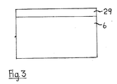
- Figure 3 is a cross-sectional view showing the product of the deposition process with the substrate body 6 supporting the deposited layer 29 of multicomponent material.
- the radiation source for the second sputtering target should be the FAB gun 17
- the FAB gun could be replaced by an alternative sputtering gun such as an ion gun.
- the deposition apparatus shown in Figure 1 could be rearranged to give other, equally effective sputtering geometries.
- the target body 9 could be of an alternative construction such as a multi-component metal target or a powder target.
- the power supply 12 and matching network for the magnetron electrode could be for radio frequency or direct current operation, If required, the substrate heater 3 could be mounted externally of the vacuum chamber.
- the oxygen feed supply 8 to the substrate body 6 could be replaced by any suitable gas feed.
- the gas feed source 21 to the gun 17 instead of argon could be any inert gas.
Landscapes
- Chemical & Material Sciences (AREA)
- Chemical Kinetics & Catalysis (AREA)
- Engineering & Computer Science (AREA)
- Materials Engineering (AREA)
- Mechanical Engineering (AREA)
- Metallurgy (AREA)
- Organic Chemistry (AREA)
- Physical Vapour Deposition (AREA)
- Physical Deposition Of Substances That Are Components Of Semiconductor Devices (AREA)
Abstract
Description
- This invention relates to a thin film deposition process. It relates particularly to the deposition of films of multicomponent materials such as lead lanthanum zirconate titanate.
- There is an increasing interest in thin film formation of multicomponent materials for specialised device applications where bulk materials or ceramics do not exhibit the necessary properties. The deposition of multicomponent materials where the volatilities of the individual components are very different has lead to much research into physical vapour (plasma) deposition techniques. The present invention was devised to aid the deposition of such materials and, in particular, the deposition of ferroelectric oxide materials such as lead lanthanum zirconate titanate (PLZT).
- Thin films of ferroelectric perovskites (such as PLZT) are of interest for electro-optic device applications, where high quality thin films of materials with large electro-optic coefficients (deposited directly onto silicon integrated circuitry) would enable higher operational switching speeds in many nonlinear optical devices.
- When a multicomponent material such as PLZT is used as the target material in a sputtering system numerous problems are encountered in depositing a crystalline thin film having the same stoichiometry as the target material. There are several main reasons for this, (1) the sputter rates and (2) the sticking coefficients of he individual components (for example, lead, lanthanum, zirconium and titanium atoms) are very different; (3) the volatilities are different (for example, that of lead is very high) and hence the more volatile component(s) can be lost from the deposited layer if the substrate has to be heated. In the case of PLZT, the temperature necessary for crystallisation in the perovskite phase is about 600°C. In addition, the possibility of negative ion resputtering of the most volatile component (this being lead in the example mentioned) can further cause a component deficiency.
- According to the present invention, there is provided a thin film deposition process, the process comprising the steps of providing a first target area on a magnetron electrode, sputtering particles from said first target area so that they fall onto a heated substrate body for forming the required deposit, simultaneously operating a sputtering gun such that further particles are dislodged from a second target area and directed towards the substrate, the two resulting particle plasmas mixing at the substrate surface such that a deposit of a predetermined chemical composition is produced.
- The said first target may be of a ceramic PLZT material. The second target may be a metal body. The metal body may be formed with adjacent areas of two metals having a common dividing line.
- The invention also comprises an apparatus for depositing multicomponent materials by a thin film deposition process.
- By way of example, a particular embodiment of the invention will now be described with reference to the accompanying drawings, in which:-
- Figure 1 is a diagram of the deposition apparatus,
- Figure 2 shows a target area from the apparatus with a common dividing line positioned between two materials carried on the target, and,
- Figure 3 is a cross-sectional view of a substrate body carrying a deposited layer of a multicomponent material which was produced in the apparatus.
- As shown in Figure 1, the apparatus comprises a vacuum deposition chamber 1 which is provided with a
gas pumping system 2. The chamber 1 includes a substrate heater 3 the temperature of which is stabilised by aheater control system 4. The heater 3 is capable of supporting asubstrate body 6 which is arranged to receive the required deposit layer. Thesubstrate body 6 surface is capable of being covered over or not covered by adjustment of amovable substrate shutter 7. - The apparatus also includes an oxygen feed pipe by which an oxygen supply may be delivered to the surface of the
substrate body 6 from anoxygen feed supply 8. - In an upper portion of the chamber 1, a ceramic
PLZT target body 9 is mounted on a magnetron electrode 11 which is adjustable in order to allow correct spacing for the sputtering system. - The magnetron electrode 11 is provided with an
electrical power supply 12 and a matching electrical network, in addition it has passages for allowing a flow of cooling water. The electrode 11 andtarget body 9 are surrounded by anearth shield 13. Thetarget body 9 may also be covered over or not covered by adjustment of amovable target shutter 14. - The magnetron electrode 11 thus gives the possibility of sputtering a single target material at a high rate of deposition onto the
substrate body 6. Theplasma 16 particles from thetarget body 9 will be directed normally towards thesubstrate body 6. - Located between the magnetron electrode 11 and the
substrate body 6, a sputtering gun which in this embodiment is a Fast Atomic Beam (FAB)gun 17 is positioned where particles from a second sputteringtarget 18 may be caused to fall on thetarget body 6. The FABgun 17 is provided with apower supply 19 and there is also agas feed source 21 capable of delivering a suitable gas such as argon or argon/oxygen to thegun 17. The second sputteringtarget 18 may be adjusted externally by variations of theangle 22 and also by variations of its position such that sputteredtarget 18 material will tend to fall on thesubstrate body 6. Theseplasma particles 23 will thus be able to mix with theplasma particles 16 fromtarget body 9 on the surface of thebody 6. - In operation of the apparatus, the
substrate body 6 is placed on the substrate heater 3 in the deposition chamber 1. The separation between thesubstrate body 6 and the PLZTceramic target body 9, mounted on the magnetron electrode 11, is adjusted to allow the correct geometry for the FAB sputtering system. The second sputteringtarget 18 which in this embodiment is made of lead is angled such that when the plasma from theFAB gun 17 irradiates the surface, the resulting sputtered lead particles will impinge on thesubstrate body 6 surface. Having set up the correct deposition geometry, the chamber 1 is evacuated by thegas pumping system 2 which is a liquid nitrogen cooled diffusion pump backed by a rotary pump. Argon is fed into the chamber at the required pressure through the FABgun 17. Theshutters 7ad 14 are placed across thetarget 9 andsubstrate 6, to allow pre-cleaning of thetargets FAB gun 17, respectively. Once the targets are clean the substrate deposition temperature is set at about 600°C on the substrate heater 3 and it is kept constant by thecontrol system 4. - The required reactive atmosphere is established using mass flow control electronics to feed argon into the
FAB gun 17 and oxygen to thesubstrate 6 surface in the required concentrations. The FABgun plasma particles 23 are adjusted to the required power levels using thepower supply 19 and themagnetron plasma particles 16 are tuned to the correct power level using thepower supply 12. Once the plasmas are stable, theshutters - The lead content of the deposited layers can be varied by altering the relative powers applied to the
FAB gun 17 and the magnetron electrode 11. The magnetron electrode 11 serves to give a high rate of deposition of theplasma particles 16 on thesubstrate body 6. Because the material of thetarget body 9 can be a multicomponent material, this can result in a variation of the composition of the material actually forming the deposit for the reasons already described. A fine compositional tuning can thus be provided by sputtering the second target material from thetarget 18 and this can be effected as necessary by independently operating thegun 17. The material from thetarget body 18 is combined at a similar energy with the lead, lanthanum, zirconium and titanium particles from thetarget body 9 where these impinge on the substrate so that the stoichiometry of the deposit can be tailored to a given application. Lead particles can thus be added as required to the deposit. A further advantage of the technique is that the lead deposit is directional so that severe contamination problems and the problems involved with handling volatile lead compounds can be avoided. - An alternative construction for the
second sputtering target 18 is shown in Figure 2. In this construction, the target area is formed withareas line 27. The two metals could be lead and titanium. This gives the possibility of further varying the composition of the deposited layer without changing the PLZT target on the magnetron electrode 11. This is done by varying the position of the FAB irradiatedarea 28. In the left hand portion of Figure 2, theirradiated area 28 is shown entirely to the left of thedividing line 27. In the middle portion of the Figure, theirradiated area 28 has been moved partially over the dividing line and in the right hand portion theirradiated area 28 is arranged equally on both sides of the dividing line. This arrangement thus allows the sputtered material at the substrate surface to contain particles from either part of thetarget 18 or any mixture of these particles. - In this manner, a large range of PLZT compositions could be obtained from a single
ceramic target body 9 coupled to a FAB sputtered lead/titanium target 18. - Figure 3 is a cross-sectional view showing the product of the deposition process with the
substrate body 6 supporting the depositedlayer 29 of multicomponent material. - The foregoing description of an embodiment of the invention has been given by way of example only and a number of modifications may be made without departing from the scope of the invention as defined in the appended claims. For instance, it is not essential that the radiation source for the second sputtering target should be the
FAB gun 17, in a different embodiment the FAB gun could be replaced by an alternative sputtering gun such as an ion gun. - In addition, the deposition apparatus shown in Figure 1 could be rearranged to give other, equally effective sputtering geometries. The
target body 9 could be of an alternative construction such as a multi-component metal target or a powder target. - The
power supply 12 and matching network for the magnetron electrode could be for radio frequency or direct current operation, If required, the substrate heater 3 could be mounted externally of the vacuum chamber. Theoxygen feed supply 8 to thesubstrate body 6 could be replaced by any suitable gas feed. Thegas feed source 21 to thegun 17 instead of argon could be any inert gas.
Claims (6)
Applications Claiming Priority (2)
| Application Number | Priority Date | Filing Date | Title |
|---|---|---|---|
| GB8718653 | 1987-08-06 | ||
| GB8718653A GB2208390B (en) | 1987-08-06 | 1987-08-06 | Thin film deposition process |
Publications (2)
| Publication Number | Publication Date |
|---|---|
| EP0302684A2 true EP0302684A2 (en) | 1989-02-08 |
| EP0302684A3 EP0302684A3 (en) | 1990-10-10 |
Family
ID=10621924
Family Applications (1)
| Application Number | Title | Priority Date | Filing Date |
|---|---|---|---|
| EP19880307070 Withdrawn EP0302684A3 (en) | 1987-08-06 | 1988-08-01 | Thin film deposition process |
Country Status (4)
| Country | Link |
|---|---|
| US (1) | US4911809A (en) |
| EP (1) | EP0302684A3 (en) |
| JP (1) | JPH01139763A (en) |
| GB (1) | GB2208390B (en) |
Cited By (4)
| Publication number | Priority date | Publication date | Assignee | Title |
|---|---|---|---|---|
| EP0396099A1 (en) * | 1989-05-02 | 1990-11-07 | Forschungszentrum Jülich Gmbh | Arrangement for removal of material from a target |
| DE3920835A1 (en) * | 1989-06-24 | 1991-01-03 | Leybold Ag | DEVICE FOR COATING SUBSTRATES |
| US5006219A (en) * | 1989-06-24 | 1991-04-09 | Leybold Aktiengesellschaft | Microwave cathode sputtering arrangement |
| EP0445897A1 (en) * | 1990-02-27 | 1991-09-11 | Fraunhofer-Gesellschaft Zur Förderung Der Angewandten Forschung E.V. | Process for deposition of thin and very thin layers |
Families Citing this family (13)
| Publication number | Priority date | Publication date | Assignee | Title |
|---|---|---|---|---|
| EP0390692A3 (en) * | 1989-03-29 | 1991-10-02 | Terumo Kabushiki Kaisha | Method of forming thin film, apparatus for forming thin film and sensor |
| EP0480409B1 (en) * | 1990-10-09 | 1994-07-13 | Nec Corporation | Method of fabricating a Ti/TiN/Al contact, with a reactive sputtering step |
| JP3048072B2 (en) * | 1991-05-25 | 2000-06-05 | ローム株式会社 | Method and apparatus for forming oxide film |
| JP2877618B2 (en) * | 1992-07-06 | 1999-03-31 | シャープ株式会社 | Method of forming ferroelectric film |
| JP3211986B2 (en) * | 1992-08-13 | 2001-09-25 | セントラル硝子株式会社 | Gray radio wave transmission type heat ray shielding glass |
| EP0600303B1 (en) * | 1992-12-01 | 2002-02-06 | Matsushita Electric Industrial Co., Ltd. | Method for fabrication of dielectric thin film |
| KR100197649B1 (en) * | 1995-09-29 | 1999-06-15 | 김영환 | Thin film depositing apparatus |
| CA2333296A1 (en) * | 1998-05-14 | 1999-11-18 | David A. Baldwin | Apparatus for sputter deposition |
| US6265033B1 (en) * | 1998-09-11 | 2001-07-24 | Donald Bennett Hilliard | Method for optically coupled vapor deposition |
| US6460243B1 (en) * | 1999-11-22 | 2002-10-08 | International Business Machines Corporation | Method of making low stress and low resistance rhodium (RH) leads |
| JP4775968B2 (en) | 2007-08-22 | 2011-09-21 | インターナショナル・ビジネス・マシーンズ・コーポレーション | Alignment film forming apparatus and method |
| WO2011093334A1 (en) | 2010-01-26 | 2011-08-04 | キヤノンアネルバ株式会社 | Film-forming method, film-forming apparatus, and apparatus for controlling the film-forming apparatus |
| EP2626442B1 (en) * | 2010-10-06 | 2020-04-15 | Ulvac, Inc. | Dielectric film formation method |
Family Cites Families (10)
| Publication number | Priority date | Publication date | Assignee | Title |
|---|---|---|---|---|
| FR1594542A (en) * | 1967-12-22 | 1970-06-08 | ||
| GB1482632A (en) * | 1974-09-11 | 1977-08-10 | Nordiko Ltd | Method and apparatus for sputtering |
| JPS57145982A (en) * | 1981-03-03 | 1982-09-09 | Toshiba Corp | Target for sputtering device |
| US4415427A (en) * | 1982-09-30 | 1983-11-15 | Gte Products Corporation | Thin film deposition by sputtering |
| GB8334369D0 (en) * | 1983-12-23 | 1984-02-01 | Ion Tech Ltd | Sputter deposition of alloys & c |
| AU566986B2 (en) * | 1984-09-04 | 1987-11-05 | Standard Oil Company, The | Deposition of passivated amorphous semi-conductor films by sputtering |
| JPS61238958A (en) * | 1985-04-15 | 1986-10-24 | Hitachi Ltd | Composite thin film formation method and device |
| US4731172A (en) * | 1985-04-18 | 1988-03-15 | Matsushita Electric Industrial Co., Ltd. | Method for sputtering multi-component thin-film |
| GB2180262B (en) * | 1985-09-05 | 1990-05-09 | Plessey Co Plc | Methods of forming substances on substrates by reactive sputtering |
| US4793908A (en) * | 1986-12-29 | 1988-12-27 | Rockwell International Corporation | Multiple ion source method and apparatus for fabricating multilayer optical films |
-
1987
- 1987-08-06 GB GB8718653A patent/GB2208390B/en not_active Expired - Lifetime
-
1988
- 1988-08-01 EP EP19880307070 patent/EP0302684A3/en not_active Withdrawn
- 1988-08-05 US US07/228,897 patent/US4911809A/en not_active Expired - Fee Related
- 1988-08-05 JP JP63194687A patent/JPH01139763A/en active Pending
Cited By (5)
| Publication number | Priority date | Publication date | Assignee | Title |
|---|---|---|---|---|
| EP0396099A1 (en) * | 1989-05-02 | 1990-11-07 | Forschungszentrum Jülich Gmbh | Arrangement for removal of material from a target |
| DE3920835A1 (en) * | 1989-06-24 | 1991-01-03 | Leybold Ag | DEVICE FOR COATING SUBSTRATES |
| US5006219A (en) * | 1989-06-24 | 1991-04-09 | Leybold Aktiengesellschaft | Microwave cathode sputtering arrangement |
| US5122252A (en) * | 1989-06-24 | 1992-06-16 | Leybold Aktiengesellschaft | Arrangement for the coating of substrates |
| EP0445897A1 (en) * | 1990-02-27 | 1991-09-11 | Fraunhofer-Gesellschaft Zur Förderung Der Angewandten Forschung E.V. | Process for deposition of thin and very thin layers |
Also Published As
| Publication number | Publication date |
|---|---|
| GB2208390A (en) | 1989-03-30 |
| GB8718653D0 (en) | 1987-09-09 |
| JPH01139763A (en) | 1989-06-01 |
| US4911809A (en) | 1990-03-27 |
| EP0302684A3 (en) | 1990-10-10 |
| GB2208390B (en) | 1991-03-27 |
Similar Documents
| Publication | Publication Date | Title |
|---|---|---|
| US4911809A (en) | Thin film deposition process | |
| US4792463A (en) | Method of producing ferroelectric thin film | |
| WO1992001081A1 (en) | Method and apparatus for co-sputtering and cross-sputtering homogeneous films | |
| Velu et al. | Ferroelectric properties of PZT thin films prepared by sputtering with stoichiometric single oxide target: Comparison between conventional and rapid thermal annealing | |
| JPH06252059A (en) | Method and apparatus for forming film | |
| US7727335B2 (en) | Device and method for the evaporative deposition of a coating material | |
| US4033843A (en) | Simple method of preparing structurally high quality PbSnTe films | |
| US4882023A (en) | Method and system for producing thin films | |
| Ameen et al. | Processing and structural characterization of ferroelectric thin films deposited by ion beam sputtering | |
| Xiao et al. | Epitaxial growth and crystallographic analyses of (Pb, La) TiO3 thin films by a multi‐ion‐beam reactive cosputtering technique | |
| Hayashi et al. | Preparation of Pb-Based Ferroelectric Thin Films by Ion-and Photo-Assisted Deposition | |
| Fukami et al. | Ferroelectric films deposited by reactive sputtering and their properties | |
| JP2547203B2 (en) | Method for forming bismuth titanate thin film | |
| Petersen et al. | Excimer laser deposition of highly oriented PLZT thin films | |
| JP2547204B2 (en) | Method for forming bismuth titanate thin film | |
| US4761300A (en) | Method of vacuum depostion of pnictide films on a substrate using a pnictide bubbler and a sputterer | |
| JP3706409B2 (en) | Method for producing composite oxide thin film | |
| Stolzer et al. | Deposition of (Bi, Sb) 2 Te 3 films by magnetron co-sputtering from two targets-first results | |
| Llewellyn et al. | TfI8: Pulsed plasma deposition of lead lanthanum zirconate titanate (PLZT) and lead lanthanum titanate (PLT) | |
| EP0321071A1 (en) | Method of producing superconducting thin films | |
| JPH06279180A (en) | Production of crystal thin film | |
| JPH04107257A (en) | Method and device for forming multicomponent compound film | |
| Kingon et al. | Sputter deposition of ferroelectric thin films | |
| Tossell et al. | Ferroelectric thin films | |
| Baumann et al. | Physical Characterization of Thin Films of Lithium Niobate Deposited on Silicon Substrates |
Legal Events
| Date | Code | Title | Description |
|---|---|---|---|
| PUAI | Public reference made under article 153(3) epc to a published international application that has entered the european phase |
Free format text: ORIGINAL CODE: 0009012 |
|
| AK | Designated contracting states |
Kind code of ref document: A2 Designated state(s): CH DE FR LI NL |
|
| PUAL | Search report despatched |
Free format text: ORIGINAL CODE: 0009013 |
|
| AK | Designated contracting states |
Kind code of ref document: A3 Designated state(s): CH DE FR LI NL |
|
| RAP1 | Party data changed (applicant data changed or rights of an application transferred) |
Owner name: GEC-MARCONI LIMITED |
|
| 17P | Request for examination filed |
Effective date: 19910321 |
|
| 17Q | First examination report despatched |
Effective date: 19930722 |
|
| STAA | Information on the status of an ep patent application or granted ep patent |
Free format text: STATUS: THE APPLICATION IS DEEMED TO BE WITHDRAWN |
|
| 18D | Application deemed to be withdrawn |
Effective date: 19931203 |