EP0301985A2 - Supraconducteur à température ambiante - Google Patents
Supraconducteur à température ambiante Download PDFInfo
- Publication number
- EP0301985A2 EP0301985A2 EP88420270A EP88420270A EP0301985A2 EP 0301985 A2 EP0301985 A2 EP 0301985A2 EP 88420270 A EP88420270 A EP 88420270A EP 88420270 A EP88420270 A EP 88420270A EP 0301985 A2 EP0301985 A2 EP 0301985A2
- Authority
- EP
- European Patent Office
- Prior art keywords
- chromium
- thin film
- thin
- film
- substrate
- Prior art date
- Legal status (The legal status is an assumption and is not a legal conclusion. Google has not performed a legal analysis and makes no representation as to the accuracy of the status listed.)
- Withdrawn
Links
- 239000002887 superconductor Substances 0.000 title claims abstract description 21
- 239000011651 chromium Substances 0.000 claims abstract description 50
- VYZAMTAEIAYCRO-UHFFFAOYSA-N Chromium Chemical compound [Cr] VYZAMTAEIAYCRO-UHFFFAOYSA-N 0.000 claims abstract description 48
- 229910052804 chromium Inorganic materials 0.000 claims abstract description 48
- 239000010409 thin film Substances 0.000 claims abstract description 47
- 239000000758 substrate Substances 0.000 claims abstract description 25
- 239000011253 protective coating Substances 0.000 claims abstract description 15
- 230000001590 oxidative effect Effects 0.000 claims abstract description 7
- 239000010408 film Substances 0.000 claims description 43
- 239000000463 material Substances 0.000 claims description 21
- 239000011248 coating agent Substances 0.000 claims description 6
- 238000000576 coating method Methods 0.000 claims description 6
- 229910000510 noble metal Inorganic materials 0.000 claims description 5
- 230000007704 transition Effects 0.000 claims description 5
- 239000004065 semiconductor Substances 0.000 claims description 4
- 230000004888 barrier function Effects 0.000 claims 1
- 229910052751 metal Inorganic materials 0.000 abstract description 2
- 239000002184 metal Substances 0.000 abstract description 2
- 235000012721 chromium Nutrition 0.000 description 40
- 230000005291 magnetic effect Effects 0.000 description 22
- 239000010445 mica Substances 0.000 description 16
- 229910052618 mica group Inorganic materials 0.000 description 16
- 230000010355 oscillation Effects 0.000 description 15
- 238000012360 testing method Methods 0.000 description 14
- FAPWRFPIFSIZLT-UHFFFAOYSA-M Sodium chloride Chemical compound [Na+].[Cl-] FAPWRFPIFSIZLT-UHFFFAOYSA-M 0.000 description 12
- 230000005292 diamagnetic effect Effects 0.000 description 9
- WFKWXMTUELFFGS-UHFFFAOYSA-N tungsten Chemical compound [W] WFKWXMTUELFFGS-UHFFFAOYSA-N 0.000 description 9
- 229910000599 Cr alloy Inorganic materials 0.000 description 7
- 239000000788 chromium alloy Substances 0.000 description 7
- 230000001681 protective effect Effects 0.000 description 7
- XEEYBQQBJWHFJM-UHFFFAOYSA-N Iron Chemical compound [Fe] XEEYBQQBJWHFJM-UHFFFAOYSA-N 0.000 description 6
- KDLHZDBZIXYQEI-UHFFFAOYSA-N Palladium Chemical compound [Pd] KDLHZDBZIXYQEI-UHFFFAOYSA-N 0.000 description 6
- 239000011780 sodium chloride Substances 0.000 description 6
- 230000005294 ferromagnetic effect Effects 0.000 description 5
- 230000005298 paramagnetic effect Effects 0.000 description 5
- 230000005290 antiferromagnetic effect Effects 0.000 description 3
- 239000004020 conductor Substances 0.000 description 3
- 230000000694 effects Effects 0.000 description 3
- 230000008020 evaporation Effects 0.000 description 3
- 238000001704 evaporation Methods 0.000 description 3
- 238000002474 experimental method Methods 0.000 description 3
- 239000011521 glass Substances 0.000 description 3
- 238000010438 heat treatment Methods 0.000 description 3
- 238000004519 manufacturing process Methods 0.000 description 3
- 229910052763 palladium Inorganic materials 0.000 description 3
- IJGRMHOSHXDMSA-UHFFFAOYSA-N Atomic nitrogen Chemical compound N#N IJGRMHOSHXDMSA-UHFFFAOYSA-N 0.000 description 2
- BQCADISMDOOEFD-UHFFFAOYSA-N Silver Chemical compound [Ag] BQCADISMDOOEFD-UHFFFAOYSA-N 0.000 description 2
- 229910045601 alloy Inorganic materials 0.000 description 2
- 239000000956 alloy Substances 0.000 description 2
- 229910052742 iron Inorganic materials 0.000 description 2
- 239000000696 magnetic material Substances 0.000 description 2
- 230000005389 magnetism Effects 0.000 description 2
- 238000005259 measurement Methods 0.000 description 2
- 229910052709 silver Inorganic materials 0.000 description 2
- 239000004332 silver Substances 0.000 description 2
- QPLDLSVMHZLSFG-UHFFFAOYSA-N Copper oxide Chemical class [Cu]=O QPLDLSVMHZLSFG-UHFFFAOYSA-N 0.000 description 1
- 229910000640 Fe alloy Inorganic materials 0.000 description 1
- 238000005275 alloying Methods 0.000 description 1
- 230000005540 biological transmission Effects 0.000 description 1
- 230000015572 biosynthetic process Effects 0.000 description 1
- 239000013590 bulk material Substances 0.000 description 1
- UPHIPHFJVNKLMR-UHFFFAOYSA-N chromium iron Chemical compound [Cr].[Fe] UPHIPHFJVNKLMR-UHFFFAOYSA-N 0.000 description 1
- 238000010276 construction Methods 0.000 description 1
- 230000007797 corrosion Effects 0.000 description 1
- 238000005260 corrosion Methods 0.000 description 1
- 238000000151 deposition Methods 0.000 description 1
- 230000008021 deposition Effects 0.000 description 1
- 238000001514 detection method Methods 0.000 description 1
- 238000006073 displacement reaction Methods 0.000 description 1
- 238000009501 film coating Methods 0.000 description 1
- 239000012212 insulator Substances 0.000 description 1
- 238000002955 isolation Methods 0.000 description 1
- 239000007788 liquid Substances 0.000 description 1
- 150000002739 metals Chemical class 0.000 description 1
- 238000012986 modification Methods 0.000 description 1
- 230000004048 modification Effects 0.000 description 1
- 229910052757 nitrogen Inorganic materials 0.000 description 1
- 239000012811 non-conductive material Substances 0.000 description 1
- -1 palladium Chemical class 0.000 description 1
- 230000000149 penetrating effect Effects 0.000 description 1
- 229910052761 rare earth metal Inorganic materials 0.000 description 1
- 230000035945 sensitivity Effects 0.000 description 1
- 230000008054 signal transmission Effects 0.000 description 1
- 239000007787 solid Substances 0.000 description 1
- 239000011343 solid material Substances 0.000 description 1
- 239000010935 stainless steel Substances 0.000 description 1
- 229910001220 stainless steel Inorganic materials 0.000 description 1
- 229910052721 tungsten Inorganic materials 0.000 description 1
- 239000010937 tungsten Substances 0.000 description 1
- 238000001771 vacuum deposition Methods 0.000 description 1
Images
Classifications
-
- H—ELECTRICITY
- H10—SEMICONDUCTOR DEVICES; ELECTRIC SOLID-STATE DEVICES NOT OTHERWISE PROVIDED FOR
- H10N—ELECTRIC SOLID-STATE DEVICES NOT OTHERWISE PROVIDED FOR
- H10N60/00—Superconducting devices
- H10N60/99—Alleged superconductivity
-
- Y—GENERAL TAGGING OF NEW TECHNOLOGICAL DEVELOPMENTS; GENERAL TAGGING OF CROSS-SECTIONAL TECHNOLOGIES SPANNING OVER SEVERAL SECTIONS OF THE IPC; TECHNICAL SUBJECTS COVERED BY FORMER USPC CROSS-REFERENCE ART COLLECTIONS [XRACs] AND DIGESTS
- Y10—TECHNICAL SUBJECTS COVERED BY FORMER USPC
- Y10S—TECHNICAL SUBJECTS COVERED BY FORMER USPC CROSS-REFERENCE ART COLLECTIONS [XRACs] AND DIGESTS
- Y10S505/00—Superconductor technology: apparatus, material, process
- Y10S505/80—Material per se process of making same
- Y10S505/801—Composition
- Y10S505/803—Magnetic
-
- Y—GENERAL TAGGING OF NEW TECHNOLOGICAL DEVELOPMENTS; GENERAL TAGGING OF CROSS-SECTIONAL TECHNOLOGIES SPANNING OVER SEVERAL SECTIONS OF THE IPC; TECHNICAL SUBJECTS COVERED BY FORMER USPC CROSS-REFERENCE ART COLLECTIONS [XRACs] AND DIGESTS
- Y10—TECHNICAL SUBJECTS COVERED BY FORMER USPC
- Y10S—TECHNICAL SUBJECTS COVERED BY FORMER USPC CROSS-REFERENCE ART COLLECTIONS [XRACs] AND DIGESTS
- Y10S505/00—Superconductor technology: apparatus, material, process
- Y10S505/80—Material per se process of making same
- Y10S505/801—Composition
- Y10S505/805—Alloy or metallic
-
- Y—GENERAL TAGGING OF NEW TECHNOLOGICAL DEVELOPMENTS; GENERAL TAGGING OF CROSS-SECTIONAL TECHNOLOGIES SPANNING OVER SEVERAL SECTIONS OF THE IPC; TECHNICAL SUBJECTS COVERED BY FORMER USPC CROSS-REFERENCE ART COLLECTIONS [XRACs] AND DIGESTS
- Y10—TECHNICAL SUBJECTS COVERED BY FORMER USPC
- Y10S—TECHNICAL SUBJECTS COVERED BY FORMER USPC CROSS-REFERENCE ART COLLECTIONS [XRACs] AND DIGESTS
- Y10S505/00—Superconductor technology: apparatus, material, process
- Y10S505/825—Apparatus per se, device per se, or process of making or operating same
- Y10S505/856—Electrical transmission or interconnection system
- Y10S505/857—Nonlinear solid-state device system or circuit
- Y10S505/86—Gating, i.e. switching circuit
- Y10S505/862—Gating, i.e. switching circuit with thin film device
Definitions
- This invention relates to a superconductor and in particular, to a device that is superconductive at room temperature.
- this invention deals with the unimpeded flow of electrically or magnetically induced currents through solid materials.
- a heat effect is produced and, as a consequence, additional energy must be provided to the system to keep the current flowing.
- a penalty which sometimes is relatively heavy must be paid in order to conduct electrical energy over any appreciable distance.
- superconductors The only class of materials which does not require constant addition of energy to keep current moving is a group of conductors known as superconductors.
- Superconductivity is not only associated with the friction free flow of electrons or of electron pairs within a material but also with the magnetic effect upon the material. All superconductors exhibit extremely high negative susceptibilities, and magnetically induced currents are established at the material surface which prevent outside magnetic fields from penetrating noticeably into the interior of the material.
- Superconductors can be used in many practical applications. Some of the best known applications involve superconducting magnets and magnetic shields. Superconductors are also used in special electronic devices such as the Josephson junction in which both superconducting and non-superconducting materials are combined for use in many computer related applications.
- a further object of the present invention is to provide a superconducting device that is capable of operating at or near room temperatures.
- Another object of the present invention is to provide a superconducting device that is manufactured from chromium or chromium alloys.
- Yet another object of the present invention is to provide special geometries that will convert a non superconducting material into a superconductor.
- a superconducting device capable of operating at or near room temperatures which includes a substrate, a thin metallic film having a negative susceptibility mounted upon the substrate and a protective coating covering the thin film for preventing it from oxidizing or otherwise becoming contaminated.
- a superconducting device capable of operating at or near room temperatures which includes a substrate, a thin metallic film having a negative susceptibility mounted upon the substrate and a protective coating covering the thin film for preventing it from oxidizing or otherwise becoming contaminated.
- multiple layers of chromium or a chromium alloy thin film having a negative susceptibility and a protective coating are placed one over the other upon a substrate to form a sandwich like structure having an increased current carrying capability.
- Chromium in its bulk state is antiferromagnetic at temperatures below the Neel temperature (311 K). At higher temperatures the material is paramagnetic.
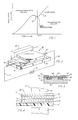
- Fig. 1 shows a resistivity curve 8 for bulk chromiums wherein resistivity is plotted against temperature. As illustrated, the resistivity of the bulk material shows a pronounced dip or "resistivity minimum" 9 centered about the Neel temperature. All bulk chromium rich alloys display similar resistivity minimums, however, the Neel temperature is displaced to either side of that of the pure chromium depending upon the properties of the alloying material.
- the high vacuum torque magnetometer noted above was used to measure the dipole moment associated with chromium thin film having thicknesses of between 1 nm and 40 nm to determine if these films exhibited ferromagnetic moments.
- the films were vacuum deposited upon non-ferromagnetic substrates. Formation of ferromagnetic surface phases in these thin chromium films were easily detected by the experimental set up, however, no evidence of any increase in the dipole moment of the thin films was noted.
- the torque magnometer system was modified by replacing the glass plate with a thin mica strip typically 0.01 mm thick which was suspended from a tungsten wire having a diameter of 0.01 mm to increase the sensitivity of the system.
- the magnetic dipole moment of a typical paramagnetic or diamagnetic thin film is so small that the dipole moment should not be expected to produce a measurable change in the period of oscillation of a thin coated mica sheet having a thickness of about 0.01 mm, a slight decrease in the period of oscillation is possible for an antiferromagnetic thin film of this nature. Any change in the period of oscillation of the system produced by an increase in the system mass due to the thin film coating could not be detected by the noted system. The detection of a measurable increase in the period of oscillation produced by the thin chromium film can only be associated with an exceptional large diamagnetic dipole moment in the film.
- a vacuum chamber as depicted in Fig. 2 was constructed to both manufacture and test thin film samples of chromium and chromium alloys having a resistivity minimum at some Neel temperature at or about room temperature.
- the apparatus includes an evaporation chamber 41 of known construction having a base 42 and a stainless steel housing 43 joined to the base to provide a sealed vacuum chamber 44.
- the equipment is coupled to a pump down system 45 capable of establishing and maintaining a high vacuum within the chamber.
- a substrate, such as a thin mica sheet 40, is suspended within the chamber upon a thin tungsten wire 50 having a diameter of about 0.01 nm and a length of about 5 cm.
- An electromagnet is mounted outside the chamber.
- the magnet shown in schematic form, includes a pair of spaced apart pole pieces 53 and 54 that are connected to a controller 51 for varying the strength of a magnetic field (H) that passes through the chamber.
- the substrate is exposed to the magnetic field established in the chamber.
- the electromagnet and the suspended substrate form part of a torque magnetometer used to measure the period of oscillation of the coated and uncoated substrates.
- a laser 56 is positioned adjacent a window 55 mounted in the chamber wall and arranged to direct a beam of light incident upon the surface of the substrate. The impinging light is reflected back through the window to a scale 57 that enables the period of oscillation of the substrate to be detected and measured accurately.
- a first tungsten heating coil 60 is mounted upon the base of the vacuum chamber and is connected by leads 61 and 62 to an exterior power supply 63.
- a second heating coil 70 is similarly mounted in the chamber and is connected to a second power supply 73 by leads 71 and 72.
- the heaters are shielded from each other by a protective plate 78.
- a chromium or chromium alloy sample 65 of known weight is placed in the first heating coil and evaporated. The evaporated chromium based material is deposited isotropically upon the substrate to produce a thin film upon the sheet.
- a second sample 75 formed of a protective coating material is placed in the second heater and is evaporated and isotropically deposited over the thin film upon the substrate.
- the coating material is selected from a transition element or a noble metal that is capable of preventing the film from becoming oxidized or otherwise contaminated when removed from the high vacuum environment.
- the chromium thin film geometry is such that the material has a negative susceptibility and operates as a superconductor at room temperature. If the film is permitted to oxidize or becomes contaminated it will lose its superconductivity.
- the fabrication and test equipment shown in Fig. 2 was used to measure the dipole moment of thin mica sheets with and without NaCl overlayers.
- the mica sheets and their tungsten wire holders were found to deviate only a few degrees from some eqilibrium position in which the sheet surface is normally parallel with the applied magnetic field.
- the period of oscillation ( ⁇ ) of the sheet produced by the magnetic field is thus easily measurable.
- the torque (T1) acting on the sheet is equal to where: I is the moment of inertia of the uncoated sheet system ⁇ 1 is the angular velocity of the uncoated sheet, and ⁇ is the angular displacement of the spin axis.
- the moment of inertia of the uncoated system differs by less than 0.1 % from that of the coated system. This change can be neglected and one value for I can be assumed for both the coated and uncoated mica sheet.
- the period of oscillation of the system changes when the sheet is coated with a thin film of chromium.
- V cr is the volume of chromium evaporated onto the mica sheet
- I is the moment of inertia of the coated system, or uncoated system
- W0 is the angular velocity of the uncoated system, without a magnetic field
- W1 is the angular momentum of the uncoated system in the magnetic field H
- W2 is the angular velocity of the chromium coated system in field H.
- a thin mica sheet having a typical thickness of 0.01 mm was suspended from a tungsten wire of 0.01 mm diameter and a length about 5 cm long was placed in the chamber between the magnetic pole piece whereby the sheet could be exposed to a magnetic force field (H) of varying strengths.
- H magnetic force field
- the susceptibility of a superconductor is typically somewhere in the range of between -10 ⁇ 5 and -1/4 ⁇ . The large negative values found for the thin chromium films tested clearly demonstrated that these films are within the range and thus superconductors.
- Example II Using the same test set up as described above in reference to Example I, the tests were repeated for a number of samples having chromium films of varying thicknesses ranging 2.8 Angstroms to 280 Angstroms. Here again it was shown that the thin chromium films remained strongly diamagnetic throughout the range. In one case, a sample having an 8 Angstrom thick film became oxidized and it changed rapidly to ferromagnetic state showing the need of protecting the thin file. Sample II was coated using a chromium iron alloy that contained 98% chromium and 2% iron. The thickness of the alloyed thin film was about 90 Angstroms. The alloyed sample was exposed to different magnetic fields and in each case the measured susceptibility showed that the alloy did not affect the negative susceptibility of the chromium base material.
- a third set of tests were conducted using the same test set up as noted above to show the effects of a protective overcoating upon samples having either a chromium or a chromium alloy thin film on a mica sheet.
- Protective overcoatings of both palladium and silver were placed over chromium based thin films having a strong negative susceptibility. It was shown that the protective coatings of these elements prevented the thin film from oxidizing and additionally served to decrease the susceptibility of the thin film thus increasing the samples superconductivity.
- a superconductive device includes a substrate 12 upon which is deposited a superconducting thin film 15.
- the substrate may be formed of either a conductive or non conductive material.
- a mica sheet that is overcoated with NaCl has been found to work well in practice.
- the thin film is preferably formed of chromium or a chromium alloy that is deposited upon the substrate to a thickness such that the film exhibits a strong negative susceptibility and thus acts as a superconductor at room temperatures.
- a protective coating 17 is next placed over the thin film to protect the film from harmful atmospheres and prevent it from oxidizing. If the film is oxidized it will lose its superconductivity.
- the protective coating may be formed of a transition element or a noble metal. Both palladium and silver coating will provide good protection for the thin film and tests have shown that these materials actually enhance the superconductivity of the thin film by making its susceptibility more negative.
- the protective coating may be replaced by an inert atmosphere in which the superconductor operates.
- the superconducting device 10 in Fig. 3 is shown in a flat configuration. It should be clear that it can be formed in any suitable configuration that might be required to make the device compatible with other devices such as a computer circuit 22.
- the substrate may be a cylindrical core with a thin film and a protective coating surrounding the core to form a transmission line of any suitable length.
- a pair of terminals 18-19 are wire bonded to the device in electric contact with the thin chromium film.
- the terminals are connected by leads 20-20 to a voltage source or power supply 21 for producing a current flow through the thin film superconductor.
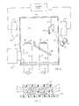
- Fig. 4 illustrates a second embodiment of the present invention wherein multiple double layered units 32-32 each containing a chromium or chromium alloy thin film 33 and protective overcoating 34 are placed one over the other upon a substrate 31 to create a sandwich like structure.
- the thickness of the thin chromium based film is controlled so that the film is superconducting.
- each thin film acts as a separate superconductor with the films combining to increase the current or signal carrying capacity of the device. Any number of layers may be placed over the substrate to meet the demands of the network being serviced.
- an electromagnet 35 containing a pair of pole pieces 36 and 37 is used to induce a current flow in the multilayered structure.
- Fig. 5 illustrates another embodiment of the invention which also includes multiple layered units 80-80 each containing a superconducting chromium thin film 81, a protective overcoating and a protective undercoating 83.
- the layered units are mounted on a glass or mica substrate 85 and are each separated by a nonconductive strip 86 which electrically isolates one unit from the other. This type of isolation may be needed in certain high frequency signal transmission applications and in certain applications acts as a control in the system to regulate the flow of current between superconducting films.
- An outer shield 87 of plastic is shown wrapped about the entire assembly to physically protect the assembly from external forces.
- Fig. 6 Another example of the invention is shown in Fig. 6. It consists of an n-type semiconductor 89, with two p-type sections 90 and 91. These p-type sections are in contact with chromium thin films 92, 93 and 95. The geometry of these thin films are as described above so that the films have a negative susceptibility and thus are capable of operating as superconductors.
- Superconductors 93, 95 which may be input and output devices, are supported by insulating films 92 and 96, and are protected against corrosion by films 97 and 99, respectively.
- These protective films can be metals like palladium, or they can be insulators.
- At least two of the p-type sections are joined by an electrical connector formed of a thin chromium film 94 and a protective coating 98.
- the thin film geometry is such as to provide the connector with superconducting properties and the coating acts to prevent the thin film from corroding or oxidizing.
Landscapes
- Superconductors And Manufacturing Methods Therefor (AREA)
- Physical Vapour Deposition (AREA)
- Containers, Films, And Cooling For Superconductive Devices (AREA)
- Shielding Devices Or Components To Electric Or Magnetic Fields (AREA)
- Inorganic Compounds Of Heavy Metals (AREA)
Applications Claiming Priority (2)
| Application Number | Priority Date | Filing Date | Title |
|---|---|---|---|
| US78758 | 1987-07-28 | ||
| US07/078,758 US4905319A (en) | 1987-07-28 | 1987-07-28 | Superconducting device including a thin chromium film with negative susceptibility |
Publications (2)
| Publication Number | Publication Date |
|---|---|
| EP0301985A2 true EP0301985A2 (fr) | 1989-02-01 |
| EP0301985A3 EP0301985A3 (fr) | 1990-01-31 |
Family
ID=22146052
Family Applications (1)
| Application Number | Title | Priority Date | Filing Date |
|---|---|---|---|
| EP88420270A Withdrawn EP0301985A3 (fr) | 1987-07-28 | 1988-07-28 | Supraconducteur à température ambiante |
Country Status (3)
| Country | Link |
|---|---|
| US (1) | US4905319A (fr) |
| EP (1) | EP0301985A3 (fr) |
| JP (1) | JPH01152260A (fr) |
Cited By (8)
| Publication number | Priority date | Publication date | Assignee | Title |
|---|---|---|---|---|
| DE4421593A1 (de) * | 1994-06-21 | 1996-01-04 | Richard Dr Sizmann | Supraleitfähige Festkörperstruktur |
| WO2012135683A1 (fr) | 2011-03-30 | 2012-10-04 | Ambature Llc | Dispositifs électriques, mécaniques, informatiques, et/ou autres dispositifs constitués de matériaux à résistance extrêmement faible |
| US8404620B2 (en) | 2011-03-30 | 2013-03-26 | Ambature, Llc | Extremely low resistance compositions and methods for creating same |
| RU2497236C2 (ru) * | 2009-05-26 | 2013-10-27 | "Текнопрайзер" Лтд. | Способ осуществления гиперпроводимости и сверхтеплопроводности |
| US8609593B2 (en) | 2009-10-02 | 2013-12-17 | Ambature, Inc. | Extremely low resistance films and methods for modifying and creating same |
| US8759257B2 (en) | 2009-10-02 | 2014-06-24 | Ambature, Inc. | High temperature superconducting films and methods for modifying and creating same |
| US8796181B2 (en) | 2010-06-04 | 2014-08-05 | Digital Signal Corporation | Extremely low resistance composition and methods for creating same |
| CN105264680A (zh) * | 2011-03-30 | 2016-01-20 | 阿姆巴托雷股份有限公司 | 由极低电阻材料形成的电气、机械、计算和/或其他设备 |
Families Citing this family (5)
| Publication number | Priority date | Publication date | Assignee | Title |
|---|---|---|---|---|
| FR2626715B1 (fr) * | 1988-02-02 | 1990-05-18 | Thomson Csf | Dispositif en couches minces de materiau supraconducteur et procede de realisation |
| FR2662856B1 (fr) * | 1990-06-01 | 1997-01-24 | Thomson Csf | Dispositifs haute frequence accordables. |
| US5304538A (en) * | 1992-03-11 | 1994-04-19 | The United States Of America As Repeated By The Administrator Of The National Aeronautics And Space Administration | Epitaxial heterojunctions of oxide semiconductors and metals on high temperature superconductors |
| US6406997B1 (en) | 1999-06-09 | 2002-06-18 | Klaus Schroder | Chromium films and chromium film overlayers |
| US6567541B1 (en) * | 2000-02-25 | 2003-05-20 | Ahbee 1, L.P. | Method and apparatus for adhesion testing of thin film materials |
Family Cites Families (3)
| Publication number | Priority date | Publication date | Assignee | Title |
|---|---|---|---|---|
| US4178602A (en) * | 1977-08-31 | 1979-12-11 | Kandyba Petr E | Thin film cryotron |
| DE3267500D1 (en) * | 1982-03-12 | 1986-01-02 | Ibm | Process for producing niobium josephson junctions |
| FR2590409B1 (fr) * | 1985-11-15 | 1987-12-11 | Commissariat Energie Atomique | Procede de fabrication d'un transistor en couches minces a grille auto-alignee par rapport au drain et a la source de celui-ci et transistor obtenu par le procede |
-
1987
- 1987-07-28 US US07/078,758 patent/US4905319A/en not_active Expired - Lifetime
-
1988
- 1988-07-28 EP EP88420270A patent/EP0301985A3/fr not_active Withdrawn
- 1988-07-28 JP JP63189524A patent/JPH01152260A/ja active Pending
Non-Patent Citations (1)
| Title |
|---|
| J. VAC. SCI. TECHNOL., vol. 10, no. 5, September/October 1973, pages 611-615, American Vacuum Society; P.H.SCHMIDT: "Superconductivity of transition metal thin films deposited by noble gas ion beam sputtering" * |
Cited By (14)
| Publication number | Priority date | Publication date | Assignee | Title |
|---|---|---|---|---|
| DE4421593A1 (de) * | 1994-06-21 | 1996-01-04 | Richard Dr Sizmann | Supraleitfähige Festkörperstruktur |
| RU2497236C2 (ru) * | 2009-05-26 | 2013-10-27 | "Текнопрайзер" Лтд. | Способ осуществления гиперпроводимости и сверхтеплопроводности |
| US9356219B2 (en) | 2009-10-02 | 2016-05-31 | Ambature, Inc. | High temperature superconducting materials and methods for modifying and creating same |
| US8609593B2 (en) | 2009-10-02 | 2013-12-17 | Ambature, Inc. | Extremely low resistance films and methods for modifying and creating same |
| US8759257B2 (en) | 2009-10-02 | 2014-06-24 | Ambature, Inc. | High temperature superconducting films and methods for modifying and creating same |
| US8796181B2 (en) | 2010-06-04 | 2014-08-05 | Digital Signal Corporation | Extremely low resistance composition and methods for creating same |
| US8404620B2 (en) | 2011-03-30 | 2013-03-26 | Ambature, Llc | Extremely low resistance compositions and methods for creating same |
| EP2691996A4 (fr) * | 2011-03-30 | 2015-01-28 | Ambature Inc | Dispositifs électriques, mécaniques, informatiques, et/ou autres dispositifs constitués de matériaux à résistance extrêmement faible |
| CN105264680A (zh) * | 2011-03-30 | 2016-01-20 | 阿姆巴托雷股份有限公司 | 由极低电阻材料形成的电气、机械、计算和/或其他设备 |
| WO2012135683A1 (fr) | 2011-03-30 | 2012-10-04 | Ambature Llc | Dispositifs électriques, mécaniques, informatiques, et/ou autres dispositifs constitués de matériaux à résistance extrêmement faible |
| RU2612847C2 (ru) * | 2011-03-30 | 2017-03-13 | ЭМБАЧЕР Инк. | Электрические, механические, вычислительные и/или другие устройства, сформированные из материалов с чрезвычайно низким сопротивлением |
| CN107611249A (zh) * | 2011-03-30 | 2018-01-19 | 阿姆巴托雷股份有限公司 | 由极低电阻材料形成的电气、机械、计算和/或其他设备 |
| CN105264680B (zh) * | 2011-03-30 | 2019-11-26 | 阿姆巴托雷股份有限公司 | 由极低电阻材料形成的电气、机械、计算和/或其他设备 |
| CN107611249B (zh) * | 2011-03-30 | 2021-11-30 | 阿姆巴托雷股份有限公司 | 由极低电阻材料形成的电气、机械、计算和/或其他设备 |
Also Published As
| Publication number | Publication date |
|---|---|
| US4905319A (en) | 1990-02-27 |
| JPH01152260A (ja) | 1989-06-14 |
| EP0301985A3 (fr) | 1990-01-31 |
Similar Documents
| Publication | Publication Date | Title |
|---|---|---|
| US4905319A (en) | Superconducting device including a thin chromium film with negative susceptibility | |
| Van Haesendonck et al. | Two-dimensional localization in thin copper films | |
| Smith et al. | Low-temperature properties of silver | |
| Vodolazov et al. | Peculiar superconducting properties of a thin film superconductor–normal metal bilayer with large ratio of resistivities | |
| Försvoll et al. | Galvanomagnetic size effects in aluminium films | |
| Eckels et al. | Magnetoresistance: the Hall effect in composite aluminium cryoconductors | |
| Mamin et al. | Charge imbalance induced by a temperature gradient in superconducting aluminum | |
| Kajimura et al. | Nonlinear electrical conductivity of superconducting films below the transition temperature | |
| Alterovitz et al. | Critical currents in sputtered copper molybdenum sulphide | |
| Stuivinga et al. | Current-induced relaxation of charge imbalance in superconducting phase-slip centers | |
| Koepke et al. | The upper critical magnetic field of lead as a function of the mean free path of the electrons | |
| Van Harlingen | Thermoelectric generation of charge imbalance at a superconductor-normal metal interface | |
| Hamasaki et al. | Critical currents in the Chevrel‐phase lead molybdenum sulfide thin films | |
| Takayama | Flux flow resistivity of superconducting thin film | |
| Yetter et al. | Flux pinning by thin chromium layers | |
| Hampshire | The critical current-density of Nb-60 at% Ti and Nb-25 at% Zr superconductors in small magnetic fields | |
| Tedrow et al. | Resolution of the spin states of a superconductor by tunneling from a ferromagnet | |
| Migliori et al. | Influence of the Proximity Effect on the Electron Thermal Conductivity of Superconducting Thin-Film Sandwiches of Indium and Thallium | |
| Dyachkov et al. | Thermal conductivity and electrical resistivity of Nb-Ti (HT-50) as a function of temperature and magnetic field | |
| Ahmedov | General relativistic thermoelectric effects in superconductors | |
| Schiller et al. | Angular dependence of the critical field of quenched thin Pb and Sn films | |
| JPH04188893A (ja) | 電気的・磁気的シールド容器及びその製造方法 | |
| Leppin et al. | Point contact spectroscopy of magnons in metals | |
| Yanson et al. | Spectroscopy of phonons in dirty superconducting contacts | |
| King et al. | Radiation damage assessment of Nb tunnel junction devices |
Legal Events
| Date | Code | Title | Description |
|---|---|---|---|
| PUAI | Public reference made under article 153(3) epc to a published international application that has entered the european phase |
Free format text: ORIGINAL CODE: 0009012 |
|
| AK | Designated contracting states |
Kind code of ref document: A2 Designated state(s): DE FR GB IT NL |
|
| PUAL | Search report despatched |
Free format text: ORIGINAL CODE: 0009013 |
|
| RHK1 | Main classification (correction) |
Ipc: H01L 39/12 |
|
| AK | Designated contracting states |
Kind code of ref document: A3 Designated state(s): DE FR GB IT NL |
|
| STAA | Information on the status of an ep patent application or granted ep patent |
Free format text: STATUS: THE APPLICATION IS DEEMED TO BE WITHDRAWN |
|
| 18D | Application deemed to be withdrawn |
Effective date: 19900801 |