EP0296511A1 - Method of fabricating a tape intended to provide circuits for electronic modules, and tape obtained by this method - Google Patents
Method of fabricating a tape intended to provide circuits for electronic modules, and tape obtained by this method Download PDFInfo
- Publication number
- EP0296511A1 EP0296511A1 EP88109743A EP88109743A EP0296511A1 EP 0296511 A1 EP0296511 A1 EP 0296511A1 EP 88109743 A EP88109743 A EP 88109743A EP 88109743 A EP88109743 A EP 88109743A EP 0296511 A1 EP0296511 A1 EP 0296511A1
- Authority
- EP
- European Patent Office
- Prior art keywords
- conductors
- strip
- sheets
- manufacturing
- circuits
- Prior art date
- Legal status (The legal status is an assumption and is not a legal conclusion. Google has not performed a legal analysis and makes no representation as to the accuracy of the status listed.)
- Granted
Links
Images


Classifications
-
- H—ELECTRICITY
- H01—ELECTRIC ELEMENTS
- H01L—SEMICONDUCTOR DEVICES NOT COVERED BY CLASS H10
- H01L21/00—Processes or apparatus adapted for the manufacture or treatment of semiconductor or solid state devices or of parts thereof
- H01L21/02—Manufacture or treatment of semiconductor devices or of parts thereof
- H01L21/04—Manufacture or treatment of semiconductor devices or of parts thereof the devices having at least one potential-jump barrier or surface barrier, e.g. PN junction, depletion layer or carrier concentration layer
- H01L21/48—Manufacture or treatment of parts, e.g. containers, prior to assembly of the devices, using processes not provided for in a single one of the subgroups H01L21/06 - H01L21/326
-
- H—ELECTRICITY
- H01—ELECTRIC ELEMENTS
- H01L—SEMICONDUCTOR DEVICES NOT COVERED BY CLASS H10
- H01L23/00—Details of semiconductor or other solid state devices
- H01L23/48—Arrangements for conducting electric current to or from the solid state body in operation, e.g. leads, terminal arrangements ; Selection of materials therefor
- H01L23/488—Arrangements for conducting electric current to or from the solid state body in operation, e.g. leads, terminal arrangements ; Selection of materials therefor consisting of soldered or bonded constructions
- H01L23/495—Lead-frames or other flat leads
- H01L23/49541—Geometry of the lead-frame
-
- B—PERFORMING OPERATIONS; TRANSPORTING
- B32—LAYERED PRODUCTS
- B32B—LAYERED PRODUCTS, i.e. PRODUCTS BUILT-UP OF STRATA OF FLAT OR NON-FLAT, e.g. CELLULAR OR HONEYCOMB, FORM
- B32B38/00—Ancillary operations in connection with laminating processes
- B32B38/18—Handling of layers or the laminate
- B32B38/1825—Handling of layers or the laminate characterised by the control or constructional features of devices for tensioning, stretching or registration
- B32B38/1833—Positioning, e.g. registration or centering
- B32B38/1841—Positioning, e.g. registration or centering during laying up
-
- H—ELECTRICITY
- H01—ELECTRIC ELEMENTS
- H01L—SEMICONDUCTOR DEVICES NOT COVERED BY CLASS H10
- H01L21/00—Processes or apparatus adapted for the manufacture or treatment of semiconductor or solid state devices or of parts thereof
- H01L21/02—Manufacture or treatment of semiconductor devices or of parts thereof
- H01L21/04—Manufacture or treatment of semiconductor devices or of parts thereof the devices having at least one potential-jump barrier or surface barrier, e.g. PN junction, depletion layer or carrier concentration layer
- H01L21/48—Manufacture or treatment of parts, e.g. containers, prior to assembly of the devices, using processes not provided for in a single one of the subgroups H01L21/06 - H01L21/326
- H01L21/4814—Conductive parts
- H01L21/4821—Flat leads, e.g. lead frames with or without insulating supports
- H01L21/4839—Assembly of a flat lead with an insulating support, e.g. for TAB
-
- H—ELECTRICITY
- H01—ELECTRIC ELEMENTS
- H01L—SEMICONDUCTOR DEVICES NOT COVERED BY CLASS H10
- H01L23/00—Details of semiconductor or other solid state devices
- H01L23/48—Arrangements for conducting electric current to or from the solid state body in operation, e.g. leads, terminal arrangements ; Selection of materials therefor
- H01L23/488—Arrangements for conducting electric current to or from the solid state body in operation, e.g. leads, terminal arrangements ; Selection of materials therefor consisting of soldered or bonded constructions
- H01L23/498—Leads, i.e. metallisations or lead-frames on insulating substrates, e.g. chip carriers
- H01L23/49861—Lead-frames fixed on or encapsulated in insulating substrates
-
- H—ELECTRICITY
- H05—ELECTRIC TECHNIQUES NOT OTHERWISE PROVIDED FOR
- H05K—PRINTED CIRCUITS; CASINGS OR CONSTRUCTIONAL DETAILS OF ELECTRIC APPARATUS; MANUFACTURE OF ASSEMBLAGES OF ELECTRICAL COMPONENTS
- H05K3/00—Apparatus or processes for manufacturing printed circuits
- H05K3/10—Apparatus or processes for manufacturing printed circuits in which conductive material is applied to the insulating support in such a manner as to form the desired conductive pattern
- H05K3/20—Apparatus or processes for manufacturing printed circuits in which conductive material is applied to the insulating support in such a manner as to form the desired conductive pattern by affixing prefabricated conductor pattern
- H05K3/202—Apparatus or processes for manufacturing printed circuits in which conductive material is applied to the insulating support in such a manner as to form the desired conductive pattern by affixing prefabricated conductor pattern using self-supporting metal foil pattern
-
- H—ELECTRICITY
- H01—ELECTRIC ELEMENTS
- H01L—SEMICONDUCTOR DEVICES NOT COVERED BY CLASS H10
- H01L2224/00—Indexing scheme for arrangements for connecting or disconnecting semiconductor or solid-state bodies and methods related thereto as covered by H01L24/00
- H01L2224/01—Means for bonding being attached to, or being formed on, the surface to be connected, e.g. chip-to-package, die-attach, "first-level" interconnects; Manufacturing methods related thereto
- H01L2224/42—Wire connectors; Manufacturing methods related thereto
- H01L2224/44—Structure, shape, material or disposition of the wire connectors prior to the connecting process
- H01L2224/45—Structure, shape, material or disposition of the wire connectors prior to the connecting process of an individual wire connector
- H01L2224/45001—Core members of the connector
- H01L2224/45099—Material
- H01L2224/451—Material with a principal constituent of the material being a metal or a metalloid, e.g. boron (B), silicon (Si), germanium (Ge), arsenic (As), antimony (Sb), tellurium (Te) and polonium (Po), and alloys thereof
- H01L2224/45138—Material with a principal constituent of the material being a metal or a metalloid, e.g. boron (B), silicon (Si), germanium (Ge), arsenic (As), antimony (Sb), tellurium (Te) and polonium (Po), and alloys thereof the principal constituent melting at a temperature of greater than or equal to 950°C and less than 1550°C
- H01L2224/45144—Gold (Au) as principal constituent
-
- H—ELECTRICITY
- H01—ELECTRIC ELEMENTS
- H01L—SEMICONDUCTOR DEVICES NOT COVERED BY CLASS H10
- H01L2224/00—Indexing scheme for arrangements for connecting or disconnecting semiconductor or solid-state bodies and methods related thereto as covered by H01L24/00
- H01L2224/01—Means for bonding being attached to, or being formed on, the surface to be connected, e.g. chip-to-package, die-attach, "first-level" interconnects; Manufacturing methods related thereto
- H01L2224/42—Wire connectors; Manufacturing methods related thereto
- H01L2224/47—Structure, shape, material or disposition of the wire connectors after the connecting process
- H01L2224/48—Structure, shape, material or disposition of the wire connectors after the connecting process of an individual wire connector
- H01L2224/4805—Shape
- H01L2224/4809—Loop shape
- H01L2224/48091—Arched
-
- H—ELECTRICITY
- H01—ELECTRIC ELEMENTS
- H01L—SEMICONDUCTOR DEVICES NOT COVERED BY CLASS H10
- H01L2224/00—Indexing scheme for arrangements for connecting or disconnecting semiconductor or solid-state bodies and methods related thereto as covered by H01L24/00
- H01L2224/01—Means for bonding being attached to, or being formed on, the surface to be connected, e.g. chip-to-package, die-attach, "first-level" interconnects; Manufacturing methods related thereto
- H01L2224/42—Wire connectors; Manufacturing methods related thereto
- H01L2224/47—Structure, shape, material or disposition of the wire connectors after the connecting process
- H01L2224/48—Structure, shape, material or disposition of the wire connectors after the connecting process of an individual wire connector
- H01L2224/481—Disposition
- H01L2224/48151—Connecting between a semiconductor or solid-state body and an item not being a semiconductor or solid-state body, e.g. chip-to-substrate, chip-to-passive
- H01L2224/48221—Connecting between a semiconductor or solid-state body and an item not being a semiconductor or solid-state body, e.g. chip-to-substrate, chip-to-passive the body and the item being stacked
- H01L2224/48225—Connecting between a semiconductor or solid-state body and an item not being a semiconductor or solid-state body, e.g. chip-to-substrate, chip-to-passive the body and the item being stacked the item being non-metallic, e.g. insulating substrate with or without metallisation
- H01L2224/48227—Connecting between a semiconductor or solid-state body and an item not being a semiconductor or solid-state body, e.g. chip-to-substrate, chip-to-passive the body and the item being stacked the item being non-metallic, e.g. insulating substrate with or without metallisation connecting the wire to a bond pad of the item
- H01L2224/48228—Connecting between a semiconductor or solid-state body and an item not being a semiconductor or solid-state body, e.g. chip-to-substrate, chip-to-passive the body and the item being stacked the item being non-metallic, e.g. insulating substrate with or without metallisation connecting the wire to a bond pad of the item the bond pad being disposed in a recess of the surface of the item
-
- H—ELECTRICITY
- H01—ELECTRIC ELEMENTS
- H01L—SEMICONDUCTOR DEVICES NOT COVERED BY CLASS H10
- H01L2224/00—Indexing scheme for arrangements for connecting or disconnecting semiconductor or solid-state bodies and methods related thereto as covered by H01L24/00
- H01L2224/01—Means for bonding being attached to, or being formed on, the surface to be connected, e.g. chip-to-package, die-attach, "first-level" interconnects; Manufacturing methods related thereto
- H01L2224/42—Wire connectors; Manufacturing methods related thereto
- H01L2224/47—Structure, shape, material or disposition of the wire connectors after the connecting process
- H01L2224/48—Structure, shape, material or disposition of the wire connectors after the connecting process of an individual wire connector
- H01L2224/484—Connecting portions
- H01L2224/4847—Connecting portions the connecting portion on the bonding area of the semiconductor or solid-state body being a wedge bond
- H01L2224/48472—Connecting portions the connecting portion on the bonding area of the semiconductor or solid-state body being a wedge bond the other connecting portion not on the bonding area also being a wedge bond, i.e. wedge-to-wedge
-
- H—ELECTRICITY
- H01—ELECTRIC ELEMENTS
- H01L—SEMICONDUCTOR DEVICES NOT COVERED BY CLASS H10
- H01L2224/00—Indexing scheme for arrangements for connecting or disconnecting semiconductor or solid-state bodies and methods related thereto as covered by H01L24/00
- H01L2224/01—Means for bonding being attached to, or being formed on, the surface to be connected, e.g. chip-to-package, die-attach, "first-level" interconnects; Manufacturing methods related thereto
- H01L2224/42—Wire connectors; Manufacturing methods related thereto
- H01L2224/47—Structure, shape, material or disposition of the wire connectors after the connecting process
- H01L2224/49—Structure, shape, material or disposition of the wire connectors after the connecting process of a plurality of wire connectors
- H01L2224/491—Disposition
- H01L2224/4912—Layout
- H01L2224/49171—Fan-out arrangements
-
- H—ELECTRICITY
- H01—ELECTRIC ELEMENTS
- H01L—SEMICONDUCTOR DEVICES NOT COVERED BY CLASS H10
- H01L24/00—Arrangements for connecting or disconnecting semiconductor or solid-state bodies; Methods or apparatus related thereto
- H01L24/01—Means for bonding being attached to, or being formed on, the surface to be connected, e.g. chip-to-package, die-attach, "first-level" interconnects; Manufacturing methods related thereto
- H01L24/42—Wire connectors; Manufacturing methods related thereto
- H01L24/47—Structure, shape, material or disposition of the wire connectors after the connecting process
- H01L24/48—Structure, shape, material or disposition of the wire connectors after the connecting process of an individual wire connector
-
- H—ELECTRICITY
- H01—ELECTRIC ELEMENTS
- H01L—SEMICONDUCTOR DEVICES NOT COVERED BY CLASS H10
- H01L24/00—Arrangements for connecting or disconnecting semiconductor or solid-state bodies; Methods or apparatus related thereto
- H01L24/01—Means for bonding being attached to, or being formed on, the surface to be connected, e.g. chip-to-package, die-attach, "first-level" interconnects; Manufacturing methods related thereto
- H01L24/42—Wire connectors; Manufacturing methods related thereto
- H01L24/47—Structure, shape, material or disposition of the wire connectors after the connecting process
- H01L24/49—Structure, shape, material or disposition of the wire connectors after the connecting process of a plurality of wire connectors
-
- H—ELECTRICITY
- H01—ELECTRIC ELEMENTS
- H01L—SEMICONDUCTOR DEVICES NOT COVERED BY CLASS H10
- H01L2924/00—Indexing scheme for arrangements or methods for connecting or disconnecting semiconductor or solid-state bodies as covered by H01L24/00
- H01L2924/0001—Technical content checked by a classifier
- H01L2924/00014—Technical content checked by a classifier the subject-matter covered by the group, the symbol of which is combined with the symbol of this group, being disclosed without further technical details
-
- H—ELECTRICITY
- H01—ELECTRIC ELEMENTS
- H01L—SEMICONDUCTOR DEVICES NOT COVERED BY CLASS H10
- H01L2924/00—Indexing scheme for arrangements or methods for connecting or disconnecting semiconductor or solid-state bodies as covered by H01L24/00
- H01L2924/01—Chemical elements
- H01L2924/01079—Gold [Au]
-
- H—ELECTRICITY
- H01—ELECTRIC ELEMENTS
- H01L—SEMICONDUCTOR DEVICES NOT COVERED BY CLASS H10
- H01L2924/00—Indexing scheme for arrangements or methods for connecting or disconnecting semiconductor or solid-state bodies as covered by H01L24/00
- H01L2924/01—Chemical elements
- H01L2924/01087—Francium [Fr]
-
- H—ELECTRICITY
- H01—ELECTRIC ELEMENTS
- H01L—SEMICONDUCTOR DEVICES NOT COVERED BY CLASS H10
- H01L2924/00—Indexing scheme for arrangements or methods for connecting or disconnecting semiconductor or solid-state bodies as covered by H01L24/00
- H01L2924/10—Details of semiconductor or other solid state devices to be connected
- H01L2924/11—Device type
- H01L2924/14—Integrated circuits
-
- H—ELECTRICITY
- H05—ELECTRIC TECHNIQUES NOT OTHERWISE PROVIDED FOR
- H05K—PRINTED CIRCUITS; CASINGS OR CONSTRUCTIONAL DETAILS OF ELECTRIC APPARATUS; MANUFACTURE OF ASSEMBLAGES OF ELECTRICAL COMPONENTS
- H05K1/00—Printed circuits
- H05K1/02—Details
- H05K1/03—Use of materials for the substrate
- H05K1/0393—Flexible materials
-
- H—ELECTRICITY
- H05—ELECTRIC TECHNIQUES NOT OTHERWISE PROVIDED FOR
- H05K—PRINTED CIRCUITS; CASINGS OR CONSTRUCTIONAL DETAILS OF ELECTRIC APPARATUS; MANUFACTURE OF ASSEMBLAGES OF ELECTRICAL COMPONENTS
- H05K2203/00—Indexing scheme relating to apparatus or processes for manufacturing printed circuits covered by H05K3/00
- H05K2203/06—Lamination
- H05K2203/063—Lamination of preperforated insulating layer
-
- H—ELECTRICITY
- H05—ELECTRIC TECHNIQUES NOT OTHERWISE PROVIDED FOR
- H05K—PRINTED CIRCUITS; CASINGS OR CONSTRUCTIONAL DETAILS OF ELECTRIC APPARATUS; MANUFACTURE OF ASSEMBLAGES OF ELECTRICAL COMPONENTS
- H05K2203/00—Indexing scheme relating to apparatus or processes for manufacturing printed circuits covered by H05K3/00
- H05K2203/15—Position of the PCB during processing
- H05K2203/1545—Continuous processing, i.e. involving rolls moving a band-like or solid carrier along a continuous production path
-
- H—ELECTRICITY
- H05—ELECTRIC TECHNIQUES NOT OTHERWISE PROVIDED FOR
- H05K—PRINTED CIRCUITS; CASINGS OR CONSTRUCTIONAL DETAILS OF ELECTRIC APPARATUS; MANUFACTURE OF ASSEMBLAGES OF ELECTRICAL COMPONENTS
- H05K3/00—Apparatus or processes for manufacturing printed circuits
- H05K3/0097—Processing two or more printed circuits simultaneously, e.g. made from a common substrate, or temporarily stacked circuit boards
-
- H—ELECTRICITY
- H05—ELECTRIC TECHNIQUES NOT OTHERWISE PROVIDED FOR
- H05K—PRINTED CIRCUITS; CASINGS OR CONSTRUCTIONAL DETAILS OF ELECTRIC APPARATUS; MANUFACTURE OF ASSEMBLAGES OF ELECTRICAL COMPONENTS
- H05K3/00—Apparatus or processes for manufacturing printed circuits
- H05K3/22—Secondary treatment of printed circuits
- H05K3/28—Applying non-metallic protective coatings
- H05K3/281—Applying non-metallic protective coatings by means of a preformed insulating foil
-
- H—ELECTRICITY
- H05—ELECTRIC TECHNIQUES NOT OTHERWISE PROVIDED FOR
- H05K—PRINTED CIRCUITS; CASINGS OR CONSTRUCTIONAL DETAILS OF ELECTRIC APPARATUS; MANUFACTURE OF ASSEMBLAGES OF ELECTRICAL COMPONENTS
- H05K3/00—Apparatus or processes for manufacturing printed circuits
- H05K3/38—Improvement of the adhesion between the insulating substrate and the metal
- H05K3/386—Improvement of the adhesion between the insulating substrate and the metal by the use of an organic polymeric bonding layer, e.g. adhesive
-
- H—ELECTRICITY
- H05—ELECTRIC TECHNIQUES NOT OTHERWISE PROVIDED FOR
- H05K—PRINTED CIRCUITS; CASINGS OR CONSTRUCTIONAL DETAILS OF ELECTRIC APPARATUS; MANUFACTURE OF ASSEMBLAGES OF ELECTRICAL COMPONENTS
- H05K3/00—Apparatus or processes for manufacturing printed circuits
- H05K3/40—Forming printed elements for providing electric connections to or between printed circuits
- H05K3/4092—Integral conductive tabs, i.e. conductive parts partly detached from the substrate
-
- Y—GENERAL TAGGING OF NEW TECHNOLOGICAL DEVELOPMENTS; GENERAL TAGGING OF CROSS-SECTIONAL TECHNOLOGIES SPANNING OVER SEVERAL SECTIONS OF THE IPC; TECHNICAL SUBJECTS COVERED BY FORMER USPC CROSS-REFERENCE ART COLLECTIONS [XRACs] AND DIGESTS
- Y10—TECHNICAL SUBJECTS COVERED BY FORMER USPC
- Y10T—TECHNICAL SUBJECTS COVERED BY FORMER US CLASSIFICATION
- Y10T156/00—Adhesive bonding and miscellaneous chemical manufacture
- Y10T156/10—Methods of surface bonding and/or assembly therefor
- Y10T156/1052—Methods of surface bonding and/or assembly therefor with cutting, punching, tearing or severing
- Y10T156/1056—Perforating lamina
- Y10T156/1057—Subsequent to assembly of laminae
-
- Y—GENERAL TAGGING OF NEW TECHNOLOGICAL DEVELOPMENTS; GENERAL TAGGING OF CROSS-SECTIONAL TECHNOLOGIES SPANNING OVER SEVERAL SECTIONS OF THE IPC; TECHNICAL SUBJECTS COVERED BY FORMER USPC CROSS-REFERENCE ART COLLECTIONS [XRACs] AND DIGESTS
- Y10—TECHNICAL SUBJECTS COVERED BY FORMER USPC
- Y10T—TECHNICAL SUBJECTS COVERED BY FORMER US CLASSIFICATION
- Y10T156/00—Adhesive bonding and miscellaneous chemical manufacture
- Y10T156/10—Methods of surface bonding and/or assembly therefor
- Y10T156/1052—Methods of surface bonding and/or assembly therefor with cutting, punching, tearing or severing
- Y10T156/108—Flash, trim or excess removal
-
- Y—GENERAL TAGGING OF NEW TECHNOLOGICAL DEVELOPMENTS; GENERAL TAGGING OF CROSS-SECTIONAL TECHNOLOGIES SPANNING OVER SEVERAL SECTIONS OF THE IPC; TECHNICAL SUBJECTS COVERED BY FORMER USPC CROSS-REFERENCE ART COLLECTIONS [XRACs] AND DIGESTS
- Y10—TECHNICAL SUBJECTS COVERED BY FORMER USPC
- Y10T—TECHNICAL SUBJECTS COVERED BY FORMER US CLASSIFICATION
- Y10T29/00—Metal working
- Y10T29/49—Method of mechanical manufacture
- Y10T29/49002—Electrical device making
- Y10T29/49117—Conductor or circuit manufacturing
- Y10T29/49124—On flat or curved insulated base, e.g., printed circuit, etc.
- Y10T29/49128—Assembling formed circuit to base
-
- Y—GENERAL TAGGING OF NEW TECHNOLOGICAL DEVELOPMENTS; GENERAL TAGGING OF CROSS-SECTIONAL TECHNOLOGIES SPANNING OVER SEVERAL SECTIONS OF THE IPC; TECHNICAL SUBJECTS COVERED BY FORMER USPC CROSS-REFERENCE ART COLLECTIONS [XRACs] AND DIGESTS
- Y10—TECHNICAL SUBJECTS COVERED BY FORMER USPC
- Y10T—TECHNICAL SUBJECTS COVERED BY FORMER US CLASSIFICATION
- Y10T29/00—Metal working
- Y10T29/49—Method of mechanical manufacture
- Y10T29/49002—Electrical device making
- Y10T29/49117—Conductor or circuit manufacturing
- Y10T29/49124—On flat or curved insulated base, e.g., printed circuit, etc.
- Y10T29/49155—Manufacturing circuit on or in base
- Y10T29/49156—Manufacturing circuit on or in base with selective destruction of conductive paths
Definitions
- the present invention which relates to flexible and thin electronic modules, relates to a process for continuously manufacturing circuits for such modules, each circuit comprising an insulating substrate and a network of thin conductors, the conductors being arranged on one side. of the substrate. At least one electronic component is also placed on one face of the circuit and connected to the conductors, the component and the circuit forming the module.
- the invention relates more particularly to a continuous manufacturing process of a ribbon, intermediate product, intended to provide a multitude of circuits for modules, as well as the ribbon obtained according to this method.
- modules are well known and, given their reduced thickness and flexibility, they are mainly intended to equip products with a small footprint.
- electronic cards also called “smart cards”, such as credit cards, parking cards, cards for telephone calls, etc., or even movements of electronic watches.
- a process for the continuous production of modules for electronic timepieces, comprising a thin circuit and electronic components is, for example, described in detail in patent FR 2 412 225.
- This process essentially consists of providing a insulating film in the form of a ribbon serving as a substrate, to glue a thin metal strip on this film, to form the networks of conductors photolithographically by eliminating the unnecessary part of the strip, the substrate and the conductors determining the circuits, to be connected to these conductors the electronic components, finally separating by stamping the modules thus obtained from the film serving as their support.
- the machining of the metal strip by photolithography includes a step of chemical attack on the metal by a solvent which, by causing ionic pollution of the insulating film, decreases the long-term reliability of the modules.
- the modules since photolithographic machining forms electrically insulated conductors, the modules, if they include an electronic component sensitive to electrostatic discharges, for example an integrated circuit, will also be very sensitive to such discharges in the phase final of their manufacture, or in storage.
- the known methods of the prior art therefore have the drawback of comprising a phase consisting in removing from the metal strip all the excess metal, in order to leave on the substrate of the circuits only conductors having their final shape, and therefore electrically isolated. .
- An object of the invention is to provide a method of continuously manufacturing a ribbon intended to supply circuits for modules which do not have this drawback.
- the manufacturing process according to the invention is particularly remarkable in that it consists: - to provide a metal strip comprising a series of openings crossing the strip right through, these openings delimiting the networks of conductors of the circuits so that each conductor remains linked to the strip by a bridge; - providing a plurality of insulating sheets, these sheets being intended to form the substrate of the circuits; and - gluing each sheet to one side of the strip using an adhesive material so that each network of conductors forms, with at least part of a sheet, a circuit, the strip and the sheets forming, on their side , tape.
- An advantage of the process according to the invention is to provide a strip which comprises, on one side, conductors which remain galvanically linked with the metal strip.
- Another object of the invention is the ribbon obtained according to the present process.
- the present invention will be described by taking as an example the continuous production of complete electronic modules for credit cards, each module being equipped in this case with a single electronic component.
- This manufacturing comprises an important intermediate stage which consists in producing a ribbon intended to supply circuits for the modules, this stage constituting the invention proper.
- the ribbon thus obtained can be advantageously used in many other fields, in particular for manufacturing electronic watch modules.
- This strip is advantageously made of nickel or ARCAP (alloy of copper, nickel and zinc).
- Such a strip referenced 1 is shown in FIG. 1.
- the length of the strip is undefined while its width is typically 35 mm. To facilitate its movement in automatic transfer machines, it can be provided with lateral perforations 2.
- the strip 1 comprises a series of openings referenced 3. These openings can advantageously be obtained by stamping, this mode of machining being clean, rapid and economical. However, if the fineness or the complexity of the openings does not allow them to be stamped, there is no disadvantage in using a photolithographic process because any trace of pollution of the metal surfaces can be easily removed by cleaning at the end of machining.
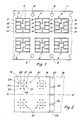
- the openings 3 are distributed over the metal strip 1 so as to form a series of identical sets 4, these sets being arranged in the longitudinal direction of the strip.
- the width of the strip shown in FIG. 1 also makes it possible to have a second series of assemblies, referenced 5, parallel to the series of assemblies 4.
- Each set 4 of openings 3 defines a network of conductors, these conductors being intended to connect the electronic component of each module to external terminals or to contact pads.
- a network comprises 8 conductors referenced from 10 to 17, each conductor remaining linked to the strip by a bridge in order to support it, these bridges respectively bearing the references 10 ′ to 17 ′.
- the bridges, in FIG. 1, are narrower than the conductors that they extend, this in order to make them stand out better, but, of course, the bridges and the conductors could have the same transverse dimension. In the case of more complex networks, a conductor could very well occupy a central position making it impossible to have a direct connection with the rest of the metal strip 1. A bridge should then be established between this conductor and a neighboring conductor for which the connection with the tape is workable.
- the sheet may advantageously be a glass or KAPTON (registered trademark) fabric, typically 125 micrometers thick, carrying on one side a thermoplastic material or a thermosetting material allowing it to be bonded hot.
- the thermoplastic and thermosetting materials can be of the type known under the name of "Hot melt” for the first, and of the type "B-Stage epoxy” for the second.
- the holes obtained for example by stamping, are distributed on the sheet so as to form a series of identical sets 30.
- each set the arrangement of the holes corresponds to the arrangement of the connections which have to connect the terminals of the electronic component to the conductors.
- the sheet 18 has, in this example, a square shape and it comprises, for reasons which will appear later, only two sets 30 arranged parallel to an axis xx ′ arbitrarily considered to be the longitudinal axis of the sheet. Two other sets, referenced 31, are also arranged on the sheet parallel to the sets 30.
- the sheet 18, which thus has four sets of holes, is applied, by its face covered with the adhesive layer, to one face of the metal strip 1 so that each set 30, 31 of holes 19, ... 27 comes opposite a network of conductors 10, ... 17. Following this sheet, another sheet, identical to the first, is placed on the strip as shown in Figure 3.
- the sheets are then glued to the strip. This is achieved by heating the sheets while pressing them against this strip. Heating, however, causes a certain shrinkage of the insulating material, this shrinkage making it difficult to use larger sheets, especially in the longitudinal direction. Of course with cold bonding the problem of shrinkage would not arise and longer sheets could be used. By cons their adhesion to the metal would be less good.
- the insulating sheets 18 can advantageously be connected one after the other by bridges 32, shown in FIG. 2, so that these sheets form a continuous insulating strip, similar to the metal strip 1, easier to handle than sheets isolated.
- the length of the bridges 32 is however greater than the distance separating two adjacent sheets on the metal strip 1 in order to allow the precise positioning of each sheet by its edges, by its holes 19, 20, .. 27, or by means of other not shown perforations provided for this purpose.
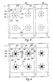
- This ribbon partially shown in Figure 3 has, in this example, a thickness of 200 micrometers and it comprises a series of identical circuits referenced 33, each circuit making it possible to obtain an electronic module.
- the module could be produced by connecting an electronic component to the circuit previously detached from the ribbon. It is however more advantageous to keep the tape intact and to deposit on the insulating face of each circuit 33, that is to say on the side of the sheet 18, the electronic component, as is shown in plan in FIG. 4, and in section along the axis VIII-VIII in FIG. 8.
- This component which in this example is an integrated circuit referenced 35, is placed in the central hole 19 of the sheet and fixed, by welding or by means of an adhesive, on the conductor 10.
- the terminals of the integrated circuit are connected, using the technique of "wire bonding", to the conductors 10, 11, ... 17 by wires 20 ′, 21 ′, ... 27 ′ passing respectively through the holes 20, 21, ... 27 of the sheet.
- the integrated circuit and the wires are still covered by a layer of opaque resin bearing the reference 36 in FIG. 5.
- the ribbon comprises at this stage of manufacture, shown in FIG. 5, two parallel rows of electronic modules, each module, referenced 40, remaining connected to the metal strip 1 by the bridges 10 ′, 11 ′, ... 17 ′, as well as by the sheet 18.
- the conductors 10, 11, .. 17 being short-circuited, the modules are protected between the electrostatic discharges.
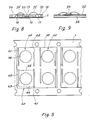
- the module 40 is separated from the metal strip 1 by cutting the last bridge 10 'along line 43, and the rest of the sheet 18 along lines 44 and 45.
- the module once detached, is then placed in a credit card so that the face of the circuit opposite to that which carries the component 35 comes flush with one face of the card so that at least part of the conductors is accessible from the outside. This part of the conductors then defines contact pads for the electrodes of the devices into which the card is intended to be inserted.
- FIG. 6 thus shows part of a metal strip 50 which comprises a set of openings 51 defining in this strip a network of conductors 52 for an analog electronic watch module, each conductor remaining linked to the strip by a bridge.
- the intermediate steps for manufacturing such modules will not be detailed since they are identical to those described for credit card modules, and they include, in particular, the steps for manufacturing a ribbon intended to provide the circuits for these modules.
- a finished watch module, but still connected to the metal strip 50, is shown in plan in Figure 7, the face of the circuit carrying the conductors being above.
- This module includes an integrated circuit 54 embedded in an opaque protective layer, a quartz resonator 55, and a coil 56 of stepping motor. These electronic components are arranged, unlike the previous module, on the face of the circuit on which the conductors 52 are located.
- Figure 9 shows this arrangement in a sectional view taken along the axis IX-IX of Figure 7, the circuit being shown without its protective layer. It is obvious that if the complexity of the circuit required it, the components could be arranged on both sides of the circuit, the sheet 53 then comprising holes making it possible to establish the connections between the conductors and the components arranged on the insulating face of the circuit.
Abstract
Description
La présente invention, qui a trait aux modules électroniques souples et de faible épaisseur, concerne un procédé de fabrication en continu des circuits pour de tels modules, chaque circuit comprenant un substrat isolant et un réseau de conducteurs minces, les conducteurs étant disposés sur une face du substrat. Au moins un composant électronique est en outre placé sur une face du circuit et connecté aux conducteurs, le composant et le circuit formant le module. L'invention concerne plus particulièrement un procédé de fabrication en continu d'un ruban, produit intermédiaire, destiné à fournir une multitude de circuits pour modules, ainsi que le ruban obtenu selon ce procédé.The present invention, which relates to flexible and thin electronic modules, relates to a process for continuously manufacturing circuits for such modules, each circuit comprising an insulating substrate and a network of thin conductors, the conductors being arranged on one side. of the substrate. At least one electronic component is also placed on one face of the circuit and connected to the conductors, the component and the circuit forming the module. The invention relates more particularly to a continuous manufacturing process of a ribbon, intermediate product, intended to provide a multitude of circuits for modules, as well as the ribbon obtained according to this method.
De tels modules sont bien connus et, étant donné leur épaisseur réduite et leur souplesse, ils sont principalement destinés à équiper des produits présentant un faible encombrement. Parmi ces produits il y a lieu de citer, en particulier, les cartes électroniques, appelées aussi "smart cards", telles que les cartes de crédit, les cartes de parking, les cartes pour les appels téléphoniques etc, ou bien encore les mouvements de montres électroniques.Such modules are well known and, given their reduced thickness and flexibility, they are mainly intended to equip products with a small footprint. Among these products, it is worth mentioning, in particular, electronic cards, also called "smart cards", such as credit cards, parking cards, cards for telephone calls, etc., or even movements of electronic watches.
Un procédé de fabrication en continu de modules pour pièces d'horlogerie électroniques, comportant un circuit mince et des composants électroniques, est, par exemple, décrit en détail dans le brevet FR 2 412 225. Ce procédé consiste essentiellement à se munir d'un film isolant en forme de ruban servant de substrat, à coller sur ce film une bande métallique mince, à former les réseaux de conducteurs par voie photolithographique en éliminant la partie inutile de la bande, le substrat et les conducteurs déterminant les circuits, à connecter à ces conducteurs les composants électroniques, enfin à séparer par étampage les modules ainsi obtenus du film leur servant de support.A process for the continuous production of modules for electronic timepieces, comprising a thin circuit and electronic components, is, for example, described in detail in
Cette manière de faire présente cependant plusieurs inconvénients. En effet, d'une part, l'usinage de la bande métallique par photolithographie, outre qu'il est long et coûteux, comporte une étape d'attaque chimique du métal par un solvant qui, en provoquant une pollution ionique du film isolant, diminue la fiabilité à long terme des modules. D'autre part, étant donné que l'usinage photolithographique forme des conducteurs électriquement isolés, les modules, s'ils comportent un composant électronique sensible aux décharges électrostatiques, par exemple un circuit intégré, seront aussi très sensibles à de telles décharges dans la phase finale de leur fabrication, ou en stockage.However, this way of doing things has several drawbacks. Indeed, on the one hand, the machining of the metal strip by photolithography, in addition to being long and costly, includes a step of chemical attack on the metal by a solvent which, by causing ionic pollution of the insulating film, decreases the long-term reliability of the modules. On the other hand, since photolithographic machining forms electrically insulated conductors, the modules, if they include an electronic component sensitive to electrostatic discharges, for example an integrated circuit, will also be very sensitive to such discharges in the phase final of their manufacture, or in storage.
Un autre procédé de fabrication en continu de circuits pour modules, présentant l'avantage de ne pas nécessiter d'attaque chimique, est décrit dans le brevet CH 608 314. Il consiste à se munir d'un film isolant, également en forme de ruban, et à coller sur ce film une bande métallique dans laquelle les conducteurs ont été préalablement découpés par étampage, chaque conducteur restant lié au reste de la bande par une de ses extrémités. Toutefois, simultanément à l'opération de collage, les conducteurs sont en outre coupés de la bande. Ainsi ce procédé, comme le précédent, fournit des circuits avec des conducteurs isolés, et donc des modules non protégés contre les chocs électriques.Another process for continuously manufacturing circuits for modules, having the advantage of not requiring chemical attack, is described in patent CH 608 314. It consists of providing an insulating film, also in the form of a tape. , and to glue on this film a metal strip in which the conductors have been previously cut by stamping, each conductor remaining linked to the rest of the strip by one of its ends. However, simultaneously with the bonding operation, the conductors are further cut from the strip. Thus this process, like the previous one, provides circuits with insulated conductors, and therefore modules not protected against electric shock.
Les procédés connus de l'art antérieur présentent donc l'inconvénient de comporter une phase consistant à enlever de la bande métallique tout le métal en excès, pour ne laisser sur le substrat des circuits que des conducteurs ayant leur forme définitive, et donc électriquement isolés.The known methods of the prior art therefore have the drawback of comprising a phase consisting in removing from the metal strip all the excess metal, in order to leave on the substrate of the circuits only conductors having their final shape, and therefore electrically isolated. .
Un but de l'invention est de proposer un procédé de fabrication en continu d'un ruban destiné à fournir des circuits pour modules ne présentant pas cet inconvénient.An object of the invention is to provide a method of continuously manufacturing a ribbon intended to supply circuits for modules which do not have this drawback.
Pour atteindre cet objectif, le procédé de fabrication selon l'invention est particulièrement remarquable en ce qu'il consiste :
- à se munir d'une bande métallique comportant une série d'ouvertures traversant la bande de part en part, ces ouvertures délimitant les réseaux de conducteurs des circuits de manière que chaque conducteur reste lié à la bande par un pont ;
- à se munir d'une pluralité de feuilles isolantes, ces feuilles étant destinées à former le substrat des circuits ; et
- à coller chaque feuille sur une face de la bande au moyen d'un matériau adhésif de manière que chaque réseau de conducteurs forme, avec au moins une partie d'une feuille, un circuit, la bande et les feuilles formant, de leur coté, le ruban.To achieve this objective, the manufacturing process according to the invention is particularly remarkable in that it consists:
- to provide a metal strip comprising a series of openings crossing the strip right through, these openings delimiting the networks of conductors of the circuits so that each conductor remains linked to the strip by a bridge;
- providing a plurality of insulating sheets, these sheets being intended to form the substrate of the circuits; and
- gluing each sheet to one side of the strip using an adhesive material so that each network of conductors forms, with at least part of a sheet, a circuit, the strip and the sheets forming, on their side , tape.
Un avantage du procédé selon l'invention est de fournir un ruban qui comporte, sur une face, des conducteurs restant liés galvaniquement avec la bande métallique.An advantage of the process according to the invention is to provide a strip which comprises, on one side, conductors which remain galvanically linked with the metal strip.
Un autre objet de l'invention est le ruban obtenu selon le présent procédé.Another object of the invention is the ribbon obtained according to the present process.
D'autres caractéristiques et avantages de la présente invention ressortiront de la description qui va suivre, faite en regard du dessin annexé et donnant, à titre explicatif mais nullement limitatif, un exemple du procédé de fabrication en continu d'un tel ruban destiné à fournir des circuits pour modules électroniques. Sur ce dessin, où les mêmes références se rapportent à des éléments analogues:
- - la figure 1 représente une partie d'une bande métallique mince pourvue d'une série d'ouvertures délimitant les conducteurs des circuits de modules électroniques destinés à équiper des cartes de crédit;
- - la figure 2 montre une feuille isolante comportant des trous pour les connexions de quatre circuits intégrés pour cartes de crédit;
- - la figure 3 est une vue montrant la feuille isolante collée sur la bande métallique, l'ensemble formant une partie du ruban selon l'invention, cette partie comportant quatre circuits ;
- - la figure 4 montre les circuits représentés sur la figure 3 sur lesquels sont disposés quatre circuits intégrés pour constituer quatre modules électroniques;
- - la figure 5 représente les modules électroniques dans leur forme finale avec les circuits intégrés protégés par une résine, chaque module étant prédécoupé mais toujours solidaire de la bande métallique;
- - la figure 6 est une vue partielle d'un bande métallique ayant des ouvertures délimitant les conducteurs d'un module destiné à équiper une montre électronique analogique;
- - la figure 7 représente ce module pour montre avec les différents éléments qui le composent ;
- - la figure 8 est une vue partielle en coupe, selon l'axe VIII-VIII, d'un des modules représentées sur la figure 4 ; et
- - la figure 9 est vue partielle en coupe, selon l'axe IX-IX, du module pour montre représenté sur la figure 7.
- - Figure 1 shows a part of a thin metal strip provided with a series of openings delimiting the conductors of the circuits of electronic modules intended to equip credit cards;
- - Figure 2 shows an insulating sheet having holes for the connections of four integrated circuits for credit cards;
- - Figure 3 is a view showing the insulating sheet bonded to the metal strip, the assembly forming a part of the tape according to the invention, this part comprising four circuits;
- - Figure 4 shows the circuits shown in Figure 3 on which are arranged four integrated circuits to form four electronic modules;
- - Figure 5 shows the electronic modules in their final form with the integrated circuits protected by a resin, each module being pre-cut but still integral with the metal strip;
- - Figure 6 is a partial view of a metal strip having openings delimiting the conductors of a module intended to equip an analog electronic watch;
- - Figure 7 shows this module for shows with the different elements that compose it;
- - Figure 8 is a partial sectional view, along the line VIII-VIII, of one of the modules shown in Figure 4; and
- FIG. 9 is a partial sectional view, along the axis IX-IX, of the watch module shown in FIG. 7.
La présente invention sera décrite en prenant comme exemple la fabrication en continu de modules électroniques complets pour cartes de crédit, chaque module étant équipé dans ce cas d'un seul composant électronique. Cette fabrication comporte une étape intermédiaire importante qui consiste à produire un ruban destiné à fournir des circuits pour les modules, cette étape constituant l'invention proprement dite. Bien entendu le ruban ainsi obtenu peut être avantageusement utilisé dans de nombreux autres domaines, en particulier pour fabriquer des modules de montres électroniques.The present invention will be described by taking as an example the continuous production of complete electronic modules for credit cards, each module being equipped in this case with a single electronic component. This manufacturing comprises an important intermediate stage which consists in producing a ribbon intended to supply circuits for the modules, this stage constituting the invention proper. Of course, the ribbon thus obtained can be advantageously used in many other fields, in particular for manufacturing electronic watch modules.
Pour obtenir le ruban par le procédé selon l'invention, puis les modules électroniques, il faut d'abord se munir d'une bande métallique mince. Cette bande, dont l'épaisseur est typiquement de 75 micromètres mais qui peut varier entre 50 et 150 micromètres, est avantageusement réalisée en nickel ou en ARCAP (alliage de cuivre, de nickel et de zinc).To obtain the ribbon by the method according to the invention, then the electronic modules, it is first necessary to have a thin metal strip. This strip, the thickness of which is typically 75 micrometers but which can vary between 50 and 150 micrometers, is advantageously made of nickel or ARCAP (alloy of copper, nickel and zinc).
Une telle bande, référencée 1, est représentée sur la figure 1. La longueur de la bande est indéfinie alors que sa largeur est typiquement de 35 mm. Pour faciliter son déplacement dans des machines de transfert automatiques, elle peut être pourvu de perforations latérales 2.Such a strip, referenced 1, is shown in FIG. 1. The length of the strip is undefined while its width is typically 35 mm. To facilitate its movement in automatic transfer machines, it can be provided with
La bande 1 comporte une série d'ouvertures référencées 3. Ces ouvertures peuvent avantageusement étre obtenues par étampage, ce mode d'usinage étant propre, rapide et économique. Cependant, si la finesse ou la complexité des ouvertures ne permet pas de les étamper, il n'y a pas d'inconvénient à utiliser un procédé photolithographique car toute trace de pollution des surfaces métalliques pourra être enlevée facilement par un nettoyage à la fin de l'usinage.The
Les ouvertures 3 sont réparties sur la bande de métal 1 de manière à former une suite d'ensembles identiques 4, ces ensembles étant disposés dans le sens longitudinal de la bande. La largeur de la bande représentée sur la figure 1 permet de disposer en outre une deuxième suite d'ensembles, référencée 5, parallèlement à la suite d'ensembles 4.The
Chaque ensemble 4 d'ouvertures 3 délimite un réseau de conducteurs, ces conducteurs étant destinés à relier le composant électronique de chaque module à des bornes extérieures ou à des plages de contact. Dans l'exemple représenté sur la figure 1 un réseau comporte 8 conducteurs référencés de 10 à 17, chaque conducteur restant lié à la bande par un pont afin de le soutenir, ces ponts portant respectivement les références 10′ à 17′. Les ponts, dans la figure 1, sont plus étroits que les conducteurs qu'ils prolongent, ceci afin de mieux les faire ressortir, mais, bien entendu, les ponts et les conducteurs pourraient avoir la même dimension transversale. Dans le cas de réseaux plus complexes, un conducteur pourrait très bien occuper une position centrale rendant impossible sa liaison directe avec le reste de la bande métallique 1. Un pont devrait alors étre établi entre ce conducteur et un conducteur voisin pour lequel la liaison avec la bande est réalisable.Each
Ensuite, il faut se munir d'une feuille isolante, référencée 18 sur la figure 2, comportant une série de trous 19, 20,..27 et dont une face est recouverte par une couche de matériau adhésif. La feuille peut avantageusement être un tissu de verre ou de KAPTON (marque déposée), typiquement de 125 micromètres d'épaisseur, portant sur une face une matière thermoplastique ou une matière thermodurcissable permettant de la coller à chaud. Les matières thermoplastique et thermodurcissable peuvent être du type connu sous le nom de "Hot melt" pour la première, et du type "B-Stage epoxy" pour la deuxième. Les trous, obtenus par exemple par étampage, sont répartis sur la feuille de manière à former une suite d'ensembles idendiques 30. Dans chaque ensemble la disposition des trous correspond à la disposition des connexions devant relier les bornes du composant électronique aux conducteurs. La feuille 18 a, dans cet exemple, une forme carrée et elle ne comporte, pour des raisons qui apparaîtront par la suite, que deux ensembles 30 disposés parallèlement à un axe xx′ considéré arbitrairement comme étant l'axe longitudinal de la feuille. Deux autres ensembles, référencés 31, sont encore disposés sur la feuille parallèlement aux ensembles 30. La feuille 18, qui comporte ainsi quatre ensembles de trous, est appliquée, par sa face recouverte de la couche adhésive, sur une face de la bande métallique 1 de manière que chaque ensemble 30, 31 de trous 19,...27 vienne en regard d'un réseau de conducteurs 10,...17. A la suite de cette feuille, une autre feuille, identique à la première, est disposée sur la bande comme le montre la figure 3. Les feuilles sont ensuite collées sur la bande. Ceci est obtenu en chauffant les feuilles tout en les pressant contre cette bande. Le chauffage provoque toutefois un certain retrait du matériau isolant, ce retrait rendant difficile l'utilisation de feuilles plus grandes, surtout dans le sens longitudinal. Bien entendu avec un collage à froid le problème du retrait ne se poserait pas et des feuilles plus longues pourraient être utilisés. Par contre leur adhérence sur le métal serait moins bonne.Then, it is necessary to provide an insulating sheet, referenced 18 in FIG. 2, comprising a series of
Les feuille isolantes 18 peuvent avantageusement être reliés les unes à la suite des autres par des ponts 32, représentés sur la figure 2, afin que ces feuilles forment une bande isolante continue, similaire à la bande métallique 1, plus facile à manipuler que des feuilles isolées. La longueur des ponts 32 est toutefois supérieure à la distance séparant deux feuilles adjacentes sur la bande métallique 1 afin de permettre le positionnement précis de chaque feuille par ses bords, par ses trous 19, 20,.. 27, ou au moyen d'autres perforations non représentées prévues à cet effet.The insulating
La bande métallique 1 et les feuilles 18 ainsi réunies forment un ruban continu, autre objet de l'invention. Ce ruban, partiellement représenté sur la figure 3 a, dans cet exemple, une épaisseur de 200 micromètres et il comporte une série de circuits identiques référencés 33, chaque circuit permettant d'obtenir un module électronique.The
Le module pourrait être réalisé en connectant un composant électronique au circuit préalablement détaché du ruban. Il est cependant plus avantageux de garder le ruban intacte et de déposer sur la face isolante de chaque circuit 33, c'est-à-dire du côté de la feuille 18, le composant électronique, ainsi que cela est représenté en plan sur la figure 4, et en coupe selon l'axe VIII-VIII sur la figure 8. Ce composant, qui est dans cet exemple un circuit intégré référencé 35, est placé dans le trou central 19 de la feuille et fixé, par une soudure ou au moyen d'une colle, sur le conducteur 10. Les bornes du circuit intégré sont connectées, en utilisant la technique du "wire bonding",aux conducteurs 10, 11,...17 par des fils 20′, 21′,... 27′ passant respectivement par les trous 20, 21,...27 de la feuille. Pour éviter tout dommage au module, le circuit intégré et les fils sont encore recouverts par une couche de résine opaque portant la référence 36 sur la figure 5.The module could be produced by connecting an electronic component to the circuit previously detached from the ribbon. It is however more advantageous to keep the tape intact and to deposit on the insulating face of each
Le ruban comporte à ce stade de fabrication, représenté sur la figure 5, deux rangées parallèles de modules électroniques, chaque module, référencé 40, restant relié à la bande métallique 1 par les ponts 10', 11',...17', ainsi que par la feuille 18. Les conducteurs 10, 11,..17 étant court-circuités, les modules sont protégés entre les décharges électrostatiques.The ribbon comprises at this stage of manufacture, shown in FIG. 5, two parallel rows of electronic modules, each module, referenced 40, remaining connected to the
Il est encore possible de tester électriquement le module 40, sans le détacher de la bande 1, en pratiquant deux ouvertures, référencées 41 et 42 sur la figure 5, de manière à couper tous les ponts à l'exception du pont 10' qui, dans le présent cas, correspond au conducteur directement connecté à la masse du circuit intégré. Les signaux sont alors appliqués et mesurés sur les conducteurs depuis la face du circuit où ils ne sont pas recouverts par la feuille isolante 18. Bien entendu les modules ne sont alors plus protégés entre les chocs électriques.It is also possible to electrically test the
Les tests terminés, le module 40 est séparé de la bande métallique 1 en coupant le dernier pont 10' suivant la ligne 43, et le reste de la feuille 18 suivant les lignes 44 et 45.When the tests are finished, the
Le module, une fois détaché, est alors placé dans une carte de crédit de manière que la face du circuit opposée à celle qui porte le composant 35 vienne à fleur d'une face de la carte afin qu'une partie au moins des conducteurs soit accessible de l'extérieur. Cette partie des conducteurs définit alors des plages de contact pour les électrodes des appareils dans lesquels la carte est destinée à étre introduite.The module, once detached, is then placed in a credit card so that the face of the circuit opposite to that which carries the
Le procédé de fabrication qui vient d'être décrit en prenant comme exemple un module électronique pour carte de crédit peut, bien entendu, être utilisé pour réaliser des modules destinés à d'autres applications, en particulier dans le domaine horloger.The manufacturing process which has just been described taking as an example an electronic module for a credit card can, of course, be used to produce modules intended for other applications, in particular in the watchmaking field.
La figure 6 montre ainsi une partie d'une bande métallique 50 qui comporte un ensemble d'ouvertures 51 définissant dans cette bande un réseau de conducteurs 52 pour un module de montre électronique analogique, chaque conducteur restant lié à la bande par un pont. Les étapes intermédiaires de fabrication de tels modules ne seront pas détaillées car elles sont identiques à celles décrites à propos des modules pour cartes de crédit, et elles comprennent, en particulier, les étapes de fabrication d'un ruban destiné à fournir les circuits pour ces modules.FIG. 6 thus shows part of a
Un module de montre terminé, mais toujours relié à la bande métallique 50, est représenté en plan sur la figure 7, la face du circuit portant les conducteurs se trouvant dessus. Ce module comprend un circuit intégré 54 enrobé dans une couche de protection opaque, un résonateur à quartz 55, et une bobine 56 de moteur pas à pas. Ces composants électroniques sont disposés, contrairement au module précédent, sur la face du circuit sur laquelle se trouvent les conducteurs 52. La figure 9 montre cette disposition dans une vue en coupe faite selon l'axe IX-IX de la figure 7, le circuit étant représenté sans sa couche de protection. Il est évident que si la complexité du circuit l'exigeait, les composants pourraient être disposés sur les deux faces du circuit, la feuille 53 comportant alors des trous permettant d'établir les connexions entre les conducteurs et les composants disposés sur la face isolante du circuit.A finished watch module, but still connected to the
Les connexions électriques entre le circuit intégré et les conducteurs sont obtenues, comme précédemment, à l'aide de fils fins en utilisant la même technique dite du "wire bonding". Mais d'autres techniques de connexion connues peuvent aussi être utilisées. Ainsi les bornes du résonateur à quartz et les fils de la bobine sont, dans ce module, directements soudés sur les conducteurs correspondants. Pour améliorer la fiabilité du module, à part le circuit intégré, d'autres composants peuvent encore être protégés par une couche de matière isolante.The electrical connections between the integrated circuit and the conductors are obtained, as before, using fine wires using the same technique known as "wire bonding". However, other known connection techniques can also be used. Thus the terminals of the quartz resonator and the wires of the coil are, in this module, directly soldered on the corresponding conductors. To improve the reliability of the module, apart from the integrated circuit, other components can also be protected by a layer of insulating material.
Il va de soi que la présente invention englobe toute modification évidente à l'homme du métier et qui pourrait être apportée au procédé de fabrication de la bande destinée à fournir les circuits des modules électroniques qui vient d'être décrit.It goes without saying that the present invention encompasses any modification obvious to a person skilled in the art and which could be made to the method of manufacturing the strip intended to supply the circuits of the electronic modules which has just been described.
Claims (13)
- à se munir d'une bande métallique mince et continue (1; 50) comportant une série d'ouvertures (3;51) traversant la bande de part en part, ces ouvertures délimitant les réseaux de conducteurs (10,... 17; 52) desdits circuits de manière que chaque conducteur reste lié à la bande par un pont (10′,...17′);
- à se munir d'une pluralité de feuilles isolantes (18; 53), ces feuilles étant destinées à former ledit substrat; et
- à coller chaque feuille (18; 53) sur une face de la bande (1; 50) au moyen d'un matériau adhésif de manière que chaque réseau de conducteurs forme, avec au moins une partie d'une feuille, un desdits circuits (33).1. A method of continuously manufacturing a ribbon intended to provide a plurality of circuits, each circuit being composed of an insulating substrate and a network of conductors arranged on one face of the substrate, these conductors being intended to be connected to at least one electronic component so that it forms with the circuit an electronic module, characterized in that it consists:
- to provide themselves with a thin and continuous metallic strip (1; 50) comprising a series of openings (3; 51) crossing the strip right through, these openings delimiting the networks of conductors (10, ... 17 ; 52) of said circuits so that each conductor remains linked to the strip by a bridge (10 ′, ... 17 ′);
- providing a plurality of insulating sheets (18; 53), these sheets being intended to form said substrate; and
- gluing each sheet (18; 53) on one side of the strip (1; 50) by means of an adhesive material so that each network of conductors forms, with at least part of a sheet, one of said circuits (33).
- une bande métallique mince et continue (1; 50) comportant une série d'ouvertures (3; 51) traversant la bande de part en part, ces ouvertures délimitant les réseaux de conducteurs (10,...17; 52) desdits circuits de manière que chaque conducteur reste lié à la bande par un pont (10′,...17′); et
- une pluralité de feuilles isolantes (18; 53) collées sur une face de ladite bande, chaque réseau de conducteurs formant, avec au moins une partie de la feuille jouant le rôle de substrat, un desdits circuits (33).11. Tape intended to supply a plurality of circuits manufactured according to the method of claim 1, each circuit being composed of an insulating substrate and a network of conductors arranged on one face of the substrate, these conductors being intended to be connected to at least one electronic component so that it forms with the circuit an electronic module, characterized in that it comprises:
- a thin and continuous metal strip (1; 50) comprising a series of openings (3; 51) passing right through the strip, these openings delimiting the networks of conductors (10, ... 17; 52) of said circuits so that each conductor remains linked to the strip by a bridge (10 ′, ... 17 ′); and
- a plurality of insulating sheets (18; 53) bonded to one face of said strip, each network of conductors forming, with at least part of the sheet acting as a substrate, one of said circuits (33).
Priority Applications (1)
| Application Number | Priority Date | Filing Date | Title |
|---|---|---|---|
| AT88109743T ATE79982T1 (en) | 1987-06-22 | 1988-06-18 | METHOD OF MANUFACTURING A RIBBON INTENDED FOR CIRCUITS FOR ELECTRONIC MODULES AND RIBBON MANUFACTURED ACCORDING TO THE PROCESS. |
Applications Claiming Priority (2)
| Application Number | Priority Date | Filing Date | Title |
|---|---|---|---|
| FR8708790 | 1987-06-22 | ||
| FR8708790A FR2616995A1 (en) | 1987-06-22 | 1987-06-22 | METHOD FOR MANUFACTURING ELECTRONIC MODULES |
Publications (2)
| Publication Number | Publication Date |
|---|---|
| EP0296511A1 true EP0296511A1 (en) | 1988-12-28 |
| EP0296511B1 EP0296511B1 (en) | 1992-08-26 |
Family
ID=9352394
Family Applications (1)
| Application Number | Title | Priority Date | Filing Date |
|---|---|---|---|
| EP88109743A Expired - Lifetime EP0296511B1 (en) | 1987-06-22 | 1988-06-18 | Method of fabricating a tape intended to provide circuits for electronic modules, and tape obtained by this method |
Country Status (9)
| Country | Link |
|---|---|
| US (1) | US5023751A (en) |
| EP (1) | EP0296511B1 (en) |
| JP (1) | JP2632992B2 (en) |
| KR (1) | KR970010149B1 (en) |
| AT (1) | ATE79982T1 (en) |
| AU (1) | AU599491B2 (en) |
| CA (1) | CA1281436C (en) |
| FR (1) | FR2616995A1 (en) |
| WO (1) | WO1988010509A1 (en) |
Cited By (8)
| Publication number | Priority date | Publication date | Assignee | Title |
|---|---|---|---|---|
| FR2673041A1 (en) * | 1991-02-19 | 1992-08-21 | Gemplus Card Int | METHOD FOR MANUFACTURING INTEGRATED CIRCUIT MICROMODULES AND CORRESPONDING MICROMODULE. |
| EP0591668A1 (en) * | 1992-09-29 | 1994-04-13 | Siemens Aktiengesellschaft | Method of mounting semiconductor integrated circuits |
| EP0674346A2 (en) * | 1994-03-22 | 1995-09-27 | Kabushiki Kaisha Toshiba | Connecting terminals for semiconductor package |
| FR2733553A1 (en) * | 1995-04-25 | 1996-10-31 | Pem Sa Protection Electrolytiq | LAMINATION DEVICE FOR SOLIDARIZING A METAL STRIP AND A STRIP OF INSULATING MATERIAL |
| WO1998006576A1 (en) * | 1996-08-15 | 1998-02-19 | Cicorel S.A. | Method and device for the lamination of foil strips |
| US6166431A (en) * | 1995-08-25 | 2000-12-26 | Kabushiki Kaisha Tishiba | Semiconductor device with a thickness of 1 MM or less |
| WO2007031241A1 (en) * | 2005-09-14 | 2007-03-22 | W.C. Heraeus Gmbh | Laminated substrate for mounting electronic parts |
| EP2109069A1 (en) * | 2008-04-11 | 2009-10-14 | Giesecke & Devrient GmbH | Method and device for implanting a chip module in a chip card body |
Families Citing this family (22)
| Publication number | Priority date | Publication date | Assignee | Title |
|---|---|---|---|---|
| US5165166A (en) * | 1987-09-29 | 1992-11-24 | Microelectronics And Computer Technology Corporation | Method of making a customizable circuitry |
| JP2751450B2 (en) * | 1989-08-28 | 1998-05-18 | セイコーエプソン株式会社 | Mounting structure of tape carrier and mounting method |
| US5231756A (en) * | 1990-05-18 | 1993-08-03 | Shinko Electric Industries Co., Ltd. | Process for manufacturing a multi-layer lead frame |
| USRE35353E (en) * | 1991-05-16 | 1996-10-22 | Shinko Electric Ind. Co, Ltd. | Process for manufacturing a multi-layer lead frame |
| US5146662A (en) * | 1991-12-30 | 1992-09-15 | Fierkens Richard H J | Lead frame cutting apparatus for various sized integrated circuit packages and method therefor |
| US5400219A (en) * | 1992-09-02 | 1995-03-21 | Eastman Kodak Company | Tape automated bonding for electrically connecting semiconductor chips to substrates |
| DE4421607A1 (en) * | 1994-06-21 | 1996-01-04 | Giesecke & Devrient Gmbh | Process for the production of data carriers |
| DE4442920C2 (en) * | 1994-12-02 | 2001-02-22 | Heraeus Gmbh W C | Process for producing a film composite |
| DE19621044A1 (en) * | 1996-05-24 | 1997-11-27 | Giesecke & Devrient Gmbh | Method for producing a card-shaped data carrier |
| DE19816066A1 (en) * | 1998-04-09 | 1999-10-14 | Philips Patentverwaltung | Foil as a carrier for integrated circuits |
| DE10318688A1 (en) * | 2003-04-24 | 2004-11-25 | W. C. Heraeus Gmbh & Co. Kg | Method for separating the electrical connection nodes in IC frames and method for producing an electronic component and frames therefor |
| DE10335015A1 (en) * | 2003-07-31 | 2005-02-24 | Robert Bosch Gmbh | Method for fixing electrical conductor tracks on a base plate and arrangement of conductor tracks and base plate |
| US20050196604A1 (en) * | 2004-03-05 | 2005-09-08 | Unifoil Corporation | Metallization process and product produced thereby |
| FR2892842B1 (en) * | 2005-10-28 | 2008-02-15 | Oberthur Card Syst Sa | PROCESS FOR MANUFACTURING A PLURALITY OF MICROCIRCUIT CARDS |
| EP1928024A1 (en) * | 2006-12-01 | 2008-06-04 | Axalto SA | Carrier film for chip modules which is adapted for automatic control of wiring and method of manufacturing chip modules |
| HK1109708A2 (en) * | 2007-04-24 | 2008-06-13 | On Track Innovations Ltd | Interface card and apparatus and process for the formation thereof |
| DE102010047912A1 (en) * | 2010-10-11 | 2012-04-12 | Polylc Gmbh & Co. Kg | Overvoltage protection for electrically conductive structures |
| CN103473593B (en) * | 2012-06-05 | 2018-10-19 | 德昌电机(深圳)有限公司 | Smart card, intelligent card contact pad carrier plate and its manufacturing method |
| USD759022S1 (en) * | 2013-03-13 | 2016-06-14 | Nagrastar Llc | Smart card interface |
| USD758372S1 (en) * | 2013-03-13 | 2016-06-07 | Nagrastar Llc | Smart card interface |
| CN104228299B (en) * | 2013-06-17 | 2015-12-02 | 成都宏明双新科技股份有限公司 | A kind of pad pasting work piece production technique |
| USD864968S1 (en) | 2015-04-30 | 2019-10-29 | Echostar Technologies L.L.C. | Smart card interface |
Citations (4)
| Publication number | Priority date | Publication date | Assignee | Title |
|---|---|---|---|---|
| DE1156131B (en) * | 1958-06-23 | 1963-10-24 | Ibm Deutschland | Method for producing an electrical conduction pattern |
| CH608314A5 (en) * | 1976-04-02 | 1978-12-29 | Ret Sa Rech Economiques Et Tec | Process for manufacturing a tape support for mounting integrated electronic components, and tape support obtained by this process |
| GB2031796A (en) * | 1978-09-29 | 1980-04-30 | Hakuto Kk | Erforations to sheet metal apparatus for sticking nonconductive tape having plating p |
| EP0201952B1 (en) * | 1985-04-12 | 1990-09-19 | Philips Composants | Method and device for manufacturing an electronic identification card |
Family Cites Families (12)
| Publication number | Priority date | Publication date | Assignee | Title |
|---|---|---|---|---|
| US1794831A (en) * | 1929-01-19 | 1931-03-03 | Lionel Corp | Multiple conductor strip and method of making the same |
| US3059320A (en) * | 1958-06-23 | 1962-10-23 | Ibm | Method of making electrical circuit |
| JPS4881063A (en) * | 1972-01-31 | 1973-10-30 | ||
| JPS4881064A (en) * | 1972-02-02 | 1973-10-30 | ||
| CH623452B (en) * | 1977-12-14 | Fontainemelon Horlogerie | METHOD OF MANUFACTURING AN ELECTRONIC CLOCK PART MODULE AND CLOCK PART MODULE OBTAINED BY IMPLEMENTATION OF THIS PROCESS. | |
| US4555291A (en) * | 1981-04-23 | 1985-11-26 | Minnesota Mining And Manufacturing Company | Method of constructing an LC network |
| JPS5858832A (en) * | 1981-09-30 | 1983-04-07 | 株式会社日立製作所 | Automatic controller for reactive power |
| JPS58100487A (en) * | 1981-12-10 | 1983-06-15 | 住友電気工業株式会社 | Method of producing printed circuit board |
| US4482874A (en) * | 1982-06-04 | 1984-11-13 | Minnesota Mining And Manufacturing Company | Method of constructing an LC network |
| JPS59125691A (en) * | 1983-01-06 | 1984-07-20 | 三洋電機株式会社 | Method of producing microstrip line |
| JPS615596A (en) * | 1984-06-19 | 1986-01-11 | 株式会社東芝 | Method of producing circuit board and circuit pattern frame used therefor |
| FR2620586A1 (en) * | 1987-09-14 | 1989-03-17 | Em Microelectronic Marin Sa | METHOD FOR MANUFACTURING ELECTRONIC MODULES, IN PARTICULAR FOR MICROCIRCUIT CARDS |
-
1987
- 1987-06-22 FR FR8708790A patent/FR2616995A1/en active Pending
-
1988
- 1988-06-06 US US07/328,252 patent/US5023751A/en not_active Expired - Lifetime
- 1988-06-06 JP JP63504423A patent/JP2632992B2/en not_active Expired - Lifetime
- 1988-06-06 KR KR1019890700313A patent/KR970010149B1/en not_active IP Right Cessation
- 1988-06-06 AU AU17974/88A patent/AU599491B2/en not_active Ceased
- 1988-06-06 WO PCT/CH1988/000102 patent/WO1988010509A1/en unknown
- 1988-06-18 EP EP88109743A patent/EP0296511B1/en not_active Expired - Lifetime
- 1988-06-18 AT AT88109743T patent/ATE79982T1/en not_active IP Right Cessation
- 1988-06-21 CA CA000569964A patent/CA1281436C/en not_active Expired - Lifetime
Patent Citations (4)
| Publication number | Priority date | Publication date | Assignee | Title |
|---|---|---|---|---|
| DE1156131B (en) * | 1958-06-23 | 1963-10-24 | Ibm Deutschland | Method for producing an electrical conduction pattern |
| CH608314A5 (en) * | 1976-04-02 | 1978-12-29 | Ret Sa Rech Economiques Et Tec | Process for manufacturing a tape support for mounting integrated electronic components, and tape support obtained by this process |
| GB2031796A (en) * | 1978-09-29 | 1980-04-30 | Hakuto Kk | Erforations to sheet metal apparatus for sticking nonconductive tape having plating p |
| EP0201952B1 (en) * | 1985-04-12 | 1990-09-19 | Philips Composants | Method and device for manufacturing an electronic identification card |
Cited By (18)
| Publication number | Priority date | Publication date | Assignee | Title |
|---|---|---|---|---|
| FR2673041A1 (en) * | 1991-02-19 | 1992-08-21 | Gemplus Card Int | METHOD FOR MANUFACTURING INTEGRATED CIRCUIT MICROMODULES AND CORRESPONDING MICROMODULE. |
| WO1992015118A1 (en) * | 1991-02-19 | 1992-09-03 | Gemplus Card International | Method for continuous assembly of patterned strips and integrated circuit micromodule obtained by said method |
| US5470411A (en) * | 1991-02-19 | 1995-11-28 | Gemplus Card International | Method for continuous assembly of patterned strips and integrated circuit micromodule obtained by said method |
| EP0734063A2 (en) * | 1991-02-19 | 1996-09-25 | Gemplus | Integrated circuit micromodule obtained by continuous assembly of patterned strips |
| EP0734063A3 (en) * | 1991-02-19 | 1997-01-29 | Gemplus Card Int | Integrated circuit micromodule obtained by continuous assembly of patterned strips |
| EP0591668A1 (en) * | 1992-09-29 | 1994-04-13 | Siemens Aktiengesellschaft | Method of mounting semiconductor integrated circuits |
| EP0674346A2 (en) * | 1994-03-22 | 1995-09-27 | Kabushiki Kaisha Toshiba | Connecting terminals for semiconductor package |
| EP0674346A3 (en) * | 1994-03-22 | 1997-02-05 | Toshiba Kk | Connecting terminals for semiconductor package. |
| WO1996034361A3 (en) * | 1995-04-25 | 1996-11-28 | Pem S A Protection Electrolyti | Laminating device for joining a metal strip and an insulating material strip |
| WO1996034361A2 (en) * | 1995-04-25 | 1996-10-31 | Pem S.A. - Protection Electrolytique Des Metaux | Laminating device for joining a metal strip and an insulating material strip |
| FR2733553A1 (en) * | 1995-04-25 | 1996-10-31 | Pem Sa Protection Electrolytiq | LAMINATION DEVICE FOR SOLIDARIZING A METAL STRIP AND A STRIP OF INSULATING MATERIAL |
| US6066231A (en) * | 1995-04-25 | 2000-05-23 | Pem S.A. Protection Electrolytique Des Metaux | Laminating device for joining a metal strip and an insulating material strip |
| US6166431A (en) * | 1995-08-25 | 2000-12-26 | Kabushiki Kaisha Tishiba | Semiconductor device with a thickness of 1 MM or less |
| US6333212B1 (en) | 1995-08-25 | 2001-12-25 | Kabushiki Kaisha Toshiba | Semiconductor device and manufacturing method thereof |
| WO1998006576A1 (en) * | 1996-08-15 | 1998-02-19 | Cicorel S.A. | Method and device for the lamination of foil strips |
| WO2007031241A1 (en) * | 2005-09-14 | 2007-03-22 | W.C. Heraeus Gmbh | Laminated substrate for mounting electronic parts |
| CN101263750B (en) * | 2005-09-14 | 2012-06-27 | W.C.贺利氏股份有限公司 | Laminated substrate for mounting electronic parts |
| EP2109069A1 (en) * | 2008-04-11 | 2009-10-14 | Giesecke & Devrient GmbH | Method and device for implanting a chip module in a chip card body |
Also Published As
| Publication number | Publication date |
|---|---|
| WO1988010509A1 (en) | 1988-12-29 |
| KR890702247A (en) | 1989-12-23 |
| FR2616995A1 (en) | 1988-12-23 |
| AU1797488A (en) | 1989-01-19 |
| US5023751A (en) | 1991-06-11 |
| KR970010149B1 (en) | 1997-06-21 |
| JP2632992B2 (en) | 1997-07-23 |
| CA1281436C (en) | 1991-03-12 |
| JPH02500231A (en) | 1990-01-25 |
| EP0296511B1 (en) | 1992-08-26 |
| ATE79982T1 (en) | 1992-09-15 |
| AU599491B2 (en) | 1990-07-19 |
Similar Documents
| Publication | Publication Date | Title |
|---|---|---|
| EP0296511B1 (en) | Method of fabricating a tape intended to provide circuits for electronic modules, and tape obtained by this method | |
| EP0094716B1 (en) | Process for connecting a semiconductor to elements of a support, particularly of a portable card | |
| EP0376062B1 (en) | Electronic module with an integrated circuit for a portable object of small dimensions, such as a card or a key, and process for manufacturing such a module | |
| EP0307773B1 (en) | Method of manufacturing electronic modules, especially for smart cards | |
| EP0128822B1 (en) | Method of producing memory cards, and cards obtained thereby | |
| EP0344058B1 (en) | Process for producing an electronic memory card, and electronic memory card obtained by using this process | |
| EP2643919B1 (en) | Method for interconnecting electronic power modules of a rotary electric machine and assembly of interconnected power modules obtained using said method | |
| FR2468209A1 (en) | PERFECTED SOLAR PANEL AND METHOD FOR MANUFACTURING THE SAME | |
| EP0044247B1 (en) | Method of producing a carrier for electronic components for the interconnection of integrated-circuit chips | |
| EP0321327B1 (en) | Method of mounting an electronic component and its electronic connections on a support | |
| FR2624652A1 (en) | METHOD FOR THE INSTALLATION ON A SUPPORT OF AN ELECTRONIC COMPONENT HAVING ITS CONTACTS | |
| EP0178977A1 (en) | Semiconductor component mounted in a plastic housing, and method for its manufacture | |
| EP0323295B1 (en) | Method for fixing an electronic component and its contacts on a carrier | |
| EP0313456A1 (en) | Copolymers useful as multifunctional additives in lubricants, and compositions containing these copolymers | |
| EP0828413B1 (en) | Electro-optical display and flexible support for devices like this to be used for electrical supply for the displays | |
| FR2762115A1 (en) | METHOD FOR INSERTING AN ELECTRONIC MODULE INTO AN ELECTRONIC MEMORY CARD BODY | |
| EP1079259B1 (en) | Manufacturing method of a display module comprising a liquid crystal cell | |
| WO2004075304A1 (en) | Method for production of a photovoltaic module and photovoltaic module produced by said method | |
| FR2568384A3 (en) | CIRCUIT SUPPORT FOR AN ELECTROMECHANICAL PENDULUM GEAR | |
| FR2531569A1 (en) | Circuit-breaker and method for the continuous manufacture of the same | |
| EP3876685A1 (en) | Prelaminated sheet for an electronic card, and methods for manufacturing such a prelaminated sheet and an electronic card comprising such a prelaminated sheet | |
| EP1928024A1 (en) | Carrier film for chip modules which is adapted for automatic control of wiring and method of manufacturing chip modules | |
| FR2531597A1 (en) | Printed circuit for heavy currents. | |
| WO2000077730A1 (en) | Electronic device comprising a chip fixed on a support and method for making same | |
| WO2008142248A2 (en) | Radiofrequency identification module, and security document incorporating same, in particular electronic passport |
Legal Events
| Date | Code | Title | Description |
|---|---|---|---|
| PUAI | Public reference made under article 153(3) epc to a published international application that has entered the european phase |
Free format text: ORIGINAL CODE: 0009012 |
|
| AK | Designated contracting states |
Kind code of ref document: A1 Designated state(s): AT CH FR IT LI NL SE |
|
| 17P | Request for examination filed |
Effective date: 19890109 |
|
| 17Q | First examination report despatched |
Effective date: 19911206 |
|
| GRAA | (expected) grant |
Free format text: ORIGINAL CODE: 0009210 |
|
| AK | Designated contracting states |
Kind code of ref document: B1 Designated state(s): AT CH FR IT LI NL SE |
|
| REF | Corresponds to: |
Ref document number: 79982 Country of ref document: AT Date of ref document: 19920915 Kind code of ref document: T |
|
| ITF | It: translation for a ep patent filed |
Owner name: ING. C. GREGORJ S.P.A. |
|
| PLBE | No opposition filed within time limit |
Free format text: ORIGINAL CODE: 0009261 |
|
| STAA | Information on the status of an ep patent application or granted ep patent |
Free format text: STATUS: NO OPPOSITION FILED WITHIN TIME LIMIT |
|
| 26N | No opposition filed | ||
| EAL | Se: european patent in force in sweden |
Ref document number: 88109743.0 |
|
| PGFP | Annual fee paid to national office [announced via postgrant information from national office to epo] |
Ref country code: AT Payment date: 20020522 Year of fee payment: 15 |
|
| PGFP | Annual fee paid to national office [announced via postgrant information from national office to epo] |
Ref country code: SE Payment date: 20020524 Year of fee payment: 15 |
|
| PGFP | Annual fee paid to national office [announced via postgrant information from national office to epo] |
Ref country code: NL Payment date: 20020529 Year of fee payment: 15 Ref country code: CH Payment date: 20020529 Year of fee payment: 15 |
|
| PGFP | Annual fee paid to national office [announced via postgrant information from national office to epo] |
Ref country code: FR Payment date: 20020627 Year of fee payment: 15 |
|
| PG25 | Lapsed in a contracting state [announced via postgrant information from national office to epo] |
Ref country code: AT Free format text: LAPSE BECAUSE OF NON-PAYMENT OF DUE FEES Effective date: 20030618 |
|
| PG25 | Lapsed in a contracting state [announced via postgrant information from national office to epo] |
Ref country code: SE Free format text: LAPSE BECAUSE OF NON-PAYMENT OF DUE FEES Effective date: 20030619 |
|
| PG25 | Lapsed in a contracting state [announced via postgrant information from national office to epo] |
Ref country code: LI Free format text: LAPSE BECAUSE OF NON-PAYMENT OF DUE FEES Effective date: 20030630 Ref country code: CH Free format text: LAPSE BECAUSE OF NON-PAYMENT OF DUE FEES Effective date: 20030630 |
|
| PG25 | Lapsed in a contracting state [announced via postgrant information from national office to epo] |
Ref country code: NL Free format text: LAPSE BECAUSE OF NON-PAYMENT OF DUE FEES Effective date: 20040101 |
|
| EUG | Se: european patent has lapsed | ||
| REG | Reference to a national code |
Ref country code: CH Ref legal event code: PL |
|
| PG25 | Lapsed in a contracting state [announced via postgrant information from national office to epo] |
Ref country code: FR Free format text: LAPSE BECAUSE OF NON-PAYMENT OF DUE FEES Effective date: 20040227 |
|
| NLV4 | Nl: lapsed or anulled due to non-payment of the annual fee |
Effective date: 20040101 |
|
| REG | Reference to a national code |
Ref country code: FR Ref legal event code: ST |
|
| PG25 | Lapsed in a contracting state [announced via postgrant information from national office to epo] |
Ref country code: IT Free format text: LAPSE BECAUSE OF NON-PAYMENT OF DUE FEES;WARNING: LAPSES OF ITALIAN PATENTS WITH EFFECTIVE DATE BEFORE 2007 MAY HAVE OCCURRED AT ANY TIME BEFORE 2007. THE CORRECT EFFECTIVE DATE MAY BE DIFFERENT FROM THE ONE RECORDED. Effective date: 20050618 |