EP0287859A2 - Verfahren und Vorrichtung zum Formen von Stiften aus extrudierbarem Material in einem Substrat - Google Patents
Verfahren und Vorrichtung zum Formen von Stiften aus extrudierbarem Material in einem Substrat Download PDFInfo
- Publication number
- EP0287859A2 EP0287859A2 EP88105085A EP88105085A EP0287859A2 EP 0287859 A2 EP0287859 A2 EP 0287859A2 EP 88105085 A EP88105085 A EP 88105085A EP 88105085 A EP88105085 A EP 88105085A EP 0287859 A2 EP0287859 A2 EP 0287859A2
- Authority
- EP
- European Patent Office
- Prior art keywords
- substrate
- pin
- die
- extrusion
- pins
- Prior art date
- Legal status (The legal status is an assumption and is not a legal conclusion. Google has not performed a legal analysis and makes no representation as to the accuracy of the status listed.)
- Granted
Links
Images


Classifications
-
- H—ELECTRICITY
- H01—ELECTRIC ELEMENTS
- H01R—ELECTRICALLY-CONDUCTIVE CONNECTIONS; STRUCTURAL ASSOCIATIONS OF A PLURALITY OF MUTUALLY-INSULATED ELECTRICAL CONNECTING ELEMENTS; COUPLING DEVICES; CURRENT COLLECTORS
- H01R43/00—Apparatus or processes specially adapted for manufacturing, assembling, maintaining, or repairing of line connectors or current collectors or for joining electric conductors
- H01R43/20—Apparatus or processes specially adapted for manufacturing, assembling, maintaining, or repairing of line connectors or current collectors or for joining electric conductors for assembling or disassembling contact members with insulating base, case or sleeve
-
- H—ELECTRICITY
- H05—ELECTRIC TECHNIQUES NOT OTHERWISE PROVIDED FOR
- H05K—PRINTED CIRCUITS; CASINGS OR CONSTRUCTIONAL DETAILS OF ELECTRIC APPARATUS; MANUFACTURE OF ASSEMBLAGES OF ELECTRICAL COMPONENTS
- H05K1/00—Printed circuits
- H05K1/02—Details
- H05K1/09—Use of materials for the conductive, e.g. metallic pattern
- H05K1/092—Dispersed materials, e.g. conductive pastes or inks
- H05K1/095—Dispersed materials, e.g. conductive pastes or inks for polymer thick films, i.e. having a permanent organic polymeric binder
-
- H—ELECTRICITY
- H05—ELECTRIC TECHNIQUES NOT OTHERWISE PROVIDED FOR
- H05K—PRINTED CIRCUITS; CASINGS OR CONSTRUCTIONAL DETAILS OF ELECTRIC APPARATUS; MANUFACTURE OF ASSEMBLAGES OF ELECTRICAL COMPONENTS
- H05K3/00—Apparatus or processes for manufacturing printed circuits
- H05K3/10—Apparatus or processes for manufacturing printed circuits in which conductive material is applied to the insulating support in such a manner as to form the desired conductive pattern
-
- H—ELECTRICITY
- H05—ELECTRIC TECHNIQUES NOT OTHERWISE PROVIDED FOR
- H05K—PRINTED CIRCUITS; CASINGS OR CONSTRUCTIONAL DETAILS OF ELECTRIC APPARATUS; MANUFACTURE OF ASSEMBLAGES OF ELECTRICAL COMPONENTS
- H05K3/00—Apparatus or processes for manufacturing printed circuits
- H05K3/40—Forming printed elements for providing electric connections to or between printed circuits
- H05K3/4038—Through-connections; Vertical interconnect access [VIA] connections
- H05K3/4053—Through-connections; Vertical interconnect access [VIA] connections by thick-film techniques
- H05K3/4069—Through-connections; Vertical interconnect access [VIA] connections by thick-film techniques for via connections in organic insulating substrates
-
- Y—GENERAL TAGGING OF NEW TECHNOLOGICAL DEVELOPMENTS; GENERAL TAGGING OF CROSS-SECTIONAL TECHNOLOGIES SPANNING OVER SEVERAL SECTIONS OF THE IPC; TECHNICAL SUBJECTS COVERED BY FORMER USPC CROSS-REFERENCE ART COLLECTIONS [XRACs] AND DIGESTS
- Y10—TECHNICAL SUBJECTS COVERED BY FORMER USPC
- Y10T—TECHNICAL SUBJECTS COVERED BY FORMER US CLASSIFICATION
- Y10T29/00—Metal working
- Y10T29/49—Method of mechanical manufacture
- Y10T29/49002—Electrical device making
- Y10T29/49117—Conductor or circuit manufacturing
- Y10T29/49124—On flat or curved insulated base, e.g., printed circuit, etc.
- Y10T29/49147—Assembling terminal to base
- Y10T29/49151—Assembling terminal to base by deforming or shaping
- Y10T29/49153—Assembling terminal to base by deforming or shaping with shaping or forcing terminal into base aperture
-
- Y—GENERAL TAGGING OF NEW TECHNOLOGICAL DEVELOPMENTS; GENERAL TAGGING OF CROSS-SECTIONAL TECHNOLOGIES SPANNING OVER SEVERAL SECTIONS OF THE IPC; TECHNICAL SUBJECTS COVERED BY FORMER USPC CROSS-REFERENCE ART COLLECTIONS [XRACs] AND DIGESTS
- Y10—TECHNICAL SUBJECTS COVERED BY FORMER USPC
- Y10T—TECHNICAL SUBJECTS COVERED BY FORMER US CLASSIFICATION
- Y10T29/00—Metal working
- Y10T29/53—Means to assemble or disassemble
- Y10T29/5313—Means to assemble electrical device
- Y10T29/532—Conductor
- Y10T29/53209—Terminal or connector
Definitions
- the field of art to which this invention relates includes, generally, the manufacture of "cards” or substrates on which are formed or mounted electrical circuits and, more particularly, includes a new and improved method and apparatus for forming a plurality of pins automatically on a substrate.
- the method used today for mounting a plurality of pins on a substrate is embodied in an apparatus having three major functions: (1) multiple pin feeding into a plurality of holes preformed in each substrate, (2) substrate feeding into this machine and (3) the attaching (or fixing) of each pin within its hole to hold it in place (called a “heading” and “bulging” operation). These functions are performed, along with other less primary operations, on seven separate stations of an eight station rotary indexing machine.
- the multiple pin feeding function involves a linear vibrator, pin feeding tube and a pin escapement mechanism.
- Several thousands of pins are dumped into a vibrating "hopper” (area). They are separated and vibrated down a "V" shaped slot into a tube.
- the tube connects the vibrator to a pin escapement device where the pins are released and pushed, as a group, into an awaiting pin holder and positioner on the index table.
- the index table rotates to a substrate loading station where one substrate is positioned to receive the pins being held in the pin holder.
- the index table rotates, again, to a "heading" and a "bulging" station where the group of pins is cold formed for retention mechanically in the holes. Finally, the index table rotates to another station for ejecting the completed substrate.
- the present invention as claimed is intended to avoid the disadvantages of the prior eight station machine entirely.
- the number of working stations is reduced from eight to one, there are no loose preformed pins to feed into very small holes, the speed of operations is increased, cost is reduced and all pins are fixed firmly in place.
- the advantages offered by the intention are mainly achieved by a method and an apparatus for forming pins of an extrudable material in a substrate.
- the method involves the steps of positioning a substrate of electrically nonconductive material in which are preformed a plurality of holes in a predetermined pattern contiguous with a pin die in which a plurality of pin channels are located in a pattern that matches the substrate holes, pressing the substrate firmly against the pin die, directing an electrically conductive material through the pin die channels and through the substrate holes, and ejecting the substrate with pins thus formed from the contiguous position with the pin die.
- the new and improved apparatus to carry out the above method includes a pin die with a plurality of pin channels in a pattern that matches the pattern of holes in a substrate, a head die to press the substrate firmly against the pin die, means to direct an electrically conductive material through the pin channels and through the holes in the substrate to form a pin in each of the substrate holes, and means to eject the pinned substrate from between the pin die and the head die.
- the particular metal being used today for substrate pins is copper, and since copper that is at least 99.90% pure has a relatively low tensile strength equal to 2250 kg/cm2, it seems ideal for use in the method and apparatus of the invention.
- the pins formed in a substrate by the present invention will be bright with clean surfaces.
- the pins tend to be discoloured and have an oxidized coating on the surfaces. Such oxidation tends to reduce electrical conductivity.
- the tolerances are maintained better, strength and hardness of the pins are higher and the ductility of the pins is lower.
- the extrusion technique that is used in the present invention involves applying a deformation load to a metal, such as copper, to cause it to flow.
- a metal such as copper
- the first known attempt at studying the flow characteristics of metals is described in a publication entitled, "Mitanderen aus dem Kaiser-Wilhelm Inst.” in 1933 by Siebel, E. and Lueg, W.
- that first work much has been done to further the extrusion process as a means of metal working and much has been written on the subject.
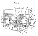
- FIG. 1 of the drawings an apparatus that is constructed and arranged in accordance with the invention is identified generally by the reference numeral 10.
- the apparatus 10 has a head die 11, a pin die 12 and an extrusion die 13.
- Extrusion is a relatively new process of fabricating metals, and the problems of suitable die material to withstand the high pressures required to extrude metal were not overcome until well into the twentieth century.
- a suitable material of which the head die 11, the pin die 12 and the extrusion die 13 may be formed is tungsten carbide, but new materials are being developed more rapidly today. Therefore, it is understood that the invention is not limited to any particular material for the dies 11, 12 and 13.
- a die will consist of two parts, a casing and a nib.
- the casing is that part shown in the drawings and identified by the reference numerals 11, 12 and 13. It is this casing that is made of tungsten carbide, whereas the nib (not visible) is the lining of the holes or apertures through which the metal is forced, and it is this lining that is made of industrial diamond.
- a substrate 14 may be formed with any number of holes in any number of patterns to fit a particular need of an electrical circuit to be formed later, only two holes 15 and 16 are shown in the drawings. As pointed out hereinabove, the number of the holes can be 360 or more.
- the number and the pattern of the plurality of holes in the substrate 14 are matched by the number and the pattern of a plurality of pin channels, illustrated by the two pin channels 17 and 18 in the pin die 12 and also by the plurality of orifices, illustrated by the two orifices 19 and 20 in the extrusion die 13.
- the holes 15 and 16 in the substrate 14, the pin channels 17 and 18 in the pin die 12 and the orifices 19 and 20 in the extrusion die 13 will be described in more detail in the description that follows.
- a new pin die 12 and a new extrusion die 13 can be installed if desired.
- the pin die 12 has a full pattern of holes (channels)
- the extrusion die 13 has a matching, full pattern of holes (orifices). Then, the holes that are not to be used for a particular group of substrates are closed off by plugs in the orifices 19 and 20 of the extrusion die 13.
- the extrusion die 13 is removable, however, by removing a plurality of bolts, represented by the two bolts 21 and 22.
- the pin channels 17 and 18 are held in position relative to the holes 15 and 16 by a plurality of guide posts, one of which is indicated by the guide post 23.
- two strips 24 and 25 are attached to the head die 11 by a plurality of threaded bolts, like the two bolts 26 and 27.
- the strips 24 and 25 are spaced apart a distance at least equal to the width of the substrate 14, so that upon first loading the substrate 14 in the apparatus, the substrate 14 will rest on flanges 28 and 29 extending along one edge of each strip 24 and 25, respectively.
- the head die 11 is moved to press the substrate 14 tightly and firmly against a support surface 30 on the pin die 12, leaving the spaces 31 and 32 above the flanges 28 and 29, respectively.
- the two spaced apart strips 24 and 25 will have to be moved if substrates having different widths are to be used in the apparatus 10, but the plurality of bolts, like the bolts 26 and 27, readily permit such an adjustment in this width.
- the head die 11, the substrate 14 and the pin die 12 are moved to shear the pin material along a line indicated by the arrow 33. Then, the head die 11, the substrate 14 and the pin die 12 are all returned to their original respective positions, and the extrusion action is begun again as the head die 11 is retracted to eject the pins.
- a substrate ejector 34 has a plurality of small, pin-like protrusions, two of which are shown and identified by the reference numerals 35 and 36, that fit in openings above each hole 15 and 16 in the substrate 14.
- the force required to eject a completed substrate 14 is minimal, and the action of the inclined surface 37 coming against the stationary surface 38 causes a surface 41 from which the pin-like protrusions 35 and 36 extend to be closed against a surface 42 on the head die 11, in order to eject the substrate 14.
- the s:ubstrate 14 will be removed by parts yet to be described, but then, the spring 40 moves the substrate ejector 34 to return it against a stop pin 43.
- the plurality of pin-like protrusions 35 and 36 will be at the surface of the substrate 14 with the ejector surface 41 resting against the head die surface 42.
- This position provides several advantages, one of which is that it ensures proper alignment of the protrusions 35 and 36 for later ejecting the completed substrate 14 and, second, it provides an indicator of the progress of the extrusion operation when the substrate ejector 34 raises up slightly and when the protrusions 35 and 36 are in the position shown in FIG. 1.
- the plurality of bolts are used to attach the apparatus of the invention 10 to a typical extrusion press, identified by the reference numeral 46.
- extrusion presses are available readily today for extruding such metals and their alloys as aluminium, copper, lead and even steel.
- a typical press for extruding copper has about a 5000 ton ram-load capacity and consists of a heavy steel shell lined with heat-resisting alloy steel and an extrusion cavity 47.
- FIG. 2 of the drawings.
- the same reference numerals are used throughout the drawings to identify the same or similar parts.
- FIG. 2 shows more of the principles of loading substrates into the apparatus 10 and of unloading the completed ones after the pinning is finished. However, this view is rotated 90 degrees from that of Fig. 1, so that in this view, the substrate 14 moves from right to left, whereas, in FIG. 1, the substrate 14 moves outwardly, toward the reader.
- the substrates having holes preformed in the desired number and pattern are arranged edge-to-edge, as indicated by the reference numeral 48.
- a suitable force is maintained on the blank substrates 48 by a slide 49 to urge them toward a stop 50.
- a substrate 48 will be in a correct position for loading onto a loading arm 51, and this correct position is identified by the numeral 52.
- the loading arm 51 moves to the left, as viewed in FIG. 2, to an approximate location, indicated now in FIG. 2 by the substrate 14.
- the movement of the loading arm 51 just described would be, looking at FIG. 1, toward the reader, in the space now occupied by the substrate 14 and between the two flanges 28 and 29 of the strips 24 and 25. At this point in its movement, the loading arm 51 moves downwardly, as viewed in FIG. 2, which leaves the blank substrate resting on the two flanges 28 and 29.
- the loading arm 51 then is retracted and raised back to its original position for receiving another blank substrate at the position 52.
- Such movements of the loading arm 51 are illustrated by the motion arrow diagram 1, 2, 3 and 4 that is adjacent to the loading arm 51.
- the motion arrow diagram is identified also by the reference numeral 53.
- a tray 54 is shown to the left in FIG. 2 that is filled in one lineal direction with completed, pinned substrates.
- the operating part of the tray 54 is two strips that are spaced apart like the strips 24 and 25 in FIG. 1.
- One of the strips, identified by numeral 55, is visible in FIG. 2.
- the strip 55 has a flange 56 that is like the flange 28 on the head die 11.
- the tray 54 has a suitable sensor to indicate when the tray is full.
- An alternative sensor is a counter at the end 57, but the preferred arrangement is a combination of both, i.e., a counter 96 at the end 57 and also a sensor 97 at the opposite end 58. By such an arrangement, the total number of completed substrates is available on the counter, and the sensor at the end 58 of the tray 54 makes the operation more automatic by providing appropriate indexing signals.
- a typical unloading operation is initiated by the head die 11 as it is raised away from the pin die 12 in order to eject a completed substrate 14.
- the tray 54 begins to move to the right, as viewed in FIG. 2, and it arrives beneath the substrate 14 as it is ejected by the protrusions 35 and 36.
- the ejection of the substrate 14 deposits it on the two flanges of the tray 54, the flange 56 begin visible in FIG. 2.
- the substrate loading arm 51 arrives with a blank substrate, and this pushes the completed substrate 14 to the left, as viewed in FIG. 2, further on the tray 54.
- the tray 54 moves out of the way, back to the left to its original starting position. Thus, one cycle of the unloading operation is completed.
- a completed, pinned substrate must be ejected.
- the loading of a blank substrate will assist the removal of the completed substrate, but before these operations are performed, the completed pins must be sheared from the extrusion material.
- a shear actuator mechanism 59 is operated.
- the distance of movement needed to perform this shearing operation is very small because of the small diameter of the extruded pins, and such distance indicated by the arrows 60 represents one-half of the distance of movement by the shear actuator mechanism 59.
- a rotatable arm 61 is connected to a suitable escapement device (not shown) by a positive attachment 62.
- a positive attachment is meant that no slippage is involved.
- the number of suitable escapement devices is large and forms no part of the present invention.
- the attachment 62 to the selected escapement device, to be appropriate for the present apparatus, is one that cannot slip, because while the diameter of each pin is on the order of 0,5 mm a large number of these pins is formed in each substrate, on the order of 360 or more. Any slippage in the actuation of the shearing mechanism will upset the timing of such operations as the loading and unloading of substrates, described above.
- a modification of the arm 61 is that it is pivotable rather than rotatable, by the attachment 62, and it may be pivoted any needed degree between 0 and 180.
- the arm 61 is either pivotable or rotatable about an axis 63, so that a cam 64 that is offset on an axis 65 will move the pin die 12 left and right along the shear line 33.
- a cam 64 that is offset on an axis 65 will move the pin die 12 left and right along the shear line 33.
- the head die 11 and the substrate 14 are moved with the pin die 12. This shearing action will be referred to in more detail hereinafter.
- roller 66 that is mounted eccentrically on an axis 67.
- the roller 66 is fitted snugly within an opening 68 in the head die 11, so that as the head die 11 is moved in the direction of the arrows 69, away from the pin die 12, and encounters the surface 38 through the substrate ejector 34, FIG. 1, the roller 66 will be at its highest point of lift for the head die 11.
- FIG. 3 of the drawings illustrates the position of the eccentric roller 66 acting within the opening 68 when the head die 11 is in its lowermost position, indicated by the arrows 73. With the roller fitting snugly within the opening 68, the head die 11 is locked securely in any location it is in.
- FIG. 4 of the drawings shows in somewhat diagrammatic form the location of the eccentric roller 66 with the head die 11, the pin die 12 and the extrusion die 13.
- the axis 67 for the roller 66 extends through its bearing supports 74 and 75, and a shaft 76 which terminates in an actuator arm 77 which is movable as indicated by the arrow 78.
- the actuator arm 77 is operated by means of a suitable escapement device (not shown), but it can be the same device, or at least timed with it. Also like the arm 61 in FIG. 2, the actuator arm 77 is movable in a rotatable manner or, preferably, in a pivotable manner.
- FIG. 5 of the drawings illustrates generally the operating principles involved in a corner locator 79 for positioning the substrate 14 accurately and for retaining it in that position laterally.
- the operating part of the corner locator 79 is a circular ring 80, also visible in FIG. 1.
- the ring 80 has cam slots 81 and 82 formed diametrically opposite each other, as illustrated.
- a cam member 83 is attached to a slide 84 and is fitted within the cam slot 81, so that as the ring 80 is moved, the slide 84 is moved as indicated by an arrow 85.
- a cam member 86 similar to the cam member 83, is attached to a slide 87 and is fitted within the cam slot 82 to move the slide 87, as indicated by an arrow 88, as the ring 80 is moved.
- Each of these slides 84 and 87 have respective ends 89 and 90 that are formed to match the corners of the substrate 14.
- the corner locator 79 is shown from the bottom of FIG. 1 looking up, and from that aspect, the view in FIG. 5 is seen.
- the substrate 14 is shown fitted within a recess having slides 91 and 92, and these slides 91 and 92 are indicated by lines 91 and 92 in FIG. 5.
- the substrate 48 is moved along the recess in the head die 11 by the loading arm 51, to an approximately correct location before it is deposited on the flanges 28 and 29, FIG. 1. Then, by adjusting the ring 80 to move the slides 84 and 87 to grip opposite corners of the blank substrate firmly, it is positioned accurately.
- the tray 54 in FIG. 2, being movable, it can be fixed in position, and the substrate loading arm 51 has an end 93 that is sufficiently ahead of the leading end 94 of the blank substrate being loaded to push the completed substrate 14 in a sliding manner along the flanges 28 and 29 to a position on the tray 54.
- a counter 96 is actuated by each edge of a substrate that passes, and a sensor 97 produces a signal causing the tray 54 to be indexed in a direction that is either toward the reader or into the figure so that a new, empty tray is moved into position for loading.
- the reference numeral 98 is used to identify a flared entrance into the space above the two flanges 28 and 29 to ensure a smooth substrate loading operation.
- FIG. 6 shows the presently preferred arrangement for forming each of the hundreds of pins by the extrusion method of the invention.
- a hollow like the hollow 99. The purpose for such a hollow 99 is to form a head 100 above the substrate 14.
- a relatively sharp edge about the hole 15 is identified by the numeral 101, while the opposite edge of the hole 15 is curved, as indicated by the numeral 102.
- Each pin channel like the pin channel 17, where it opens at the substrate support surface 30, is countersunk, as indicated by the numeral 103, to permit the formation of a bulge 104. Between the pin head 100 against the upper surface of the substrate 14 and the bulge 104 against the lower, or opposite, surface, each pin formed in the substrate 14 by the invention is fixed firmly in place.
- the line between the pin die 12 and the extrusion die 13 is the shear line 33.
- each orifice furthermost from the shear line 33 is countersunk to form a slip line field 105 to permit extruding at higher speeds and better "working" of the metal being extruded.
- the extrusion cavity 47 in the extrusion press 46 contains the usual ram 106 that is actuated, as indicated by the numeral 107. The details of such an extrusion press 46 are not included because they are well known in that art.
- FIG. 7 of the drawings illustrates an important modification of the invention, as will be explained in more detail presently.
- the essential differences in structure are embodied in the extrusion die 13 as passages 108 adjacent each orifice, such as the orifice 19.
- Each of the passages is located so that as the pin die 12 is moved to shear the pin material along the line 33, the sheared end of each pin will stop over one of the passages 108.
- the passages 108 are all connected to a suitable source of fluid under pressure.
- a suitable source of fluid under pressure is used to eject the pins from the pin die 12.
- Such fluid is at least used to assist in the otherwise usual ejection of the pins and completed substrate.
- An example of a suitable fluid is air, although in some instances of use of the invention a liquid would be more appropriate.
- FIG. 8 of the drawings illustrates still another modification of the invention.
- An important omission from the structure of FIG. 8 is the extrusion die 13 shown in all the other figures.
- the structure in FIG. 8 includes the protrusions 35 and 36, FIG. 1.
- Yet another modification of the apparatus according to the present invention is seen in the arcuate holes 15 and 16 in the substrate 14.
- the formation of the pin head 100 provides two significant purposes, one of which is identified hereinabove and that involves a later use of the pinned substrates.
- a "land" of electrically conductive material is formed around these heads 100 to provide the required electrical connection.
- the other significant purpose of the head 100 is that, along with the bulge 104, the pin is fixed in place firmly. Therefore, as the pin diameters are made smaller and smaller, the head 100 will become smaller also, to a point where its effectiveness for fixing the pin in place mechanically is not sufficient. Whereupon, a structure as illustrated in FIG. 8 provides more mechanical strength in the head 100.
- the particular degree of curvature of the arcuate holes 15 and 16 is not as important as the result which they admit, which is the increased strength of the head 100.
- the arcuate holes 15 and 16 can be curved adjacent the two surfaces of the substrate 14, like the curve 102 shown in FIG. 6, or like the degree of curvature shown in FIG. 8, which is a more continuous curve 109 from one surface of the substrate to the other. The curve 109 will maximize the strength of the head 100.
- Such a plastic material is suitable for pins as contemplated by the invention under certain conditions.
- the use of such a mixture in larger diameter pins is likely to produce spots of either nonconductivity or high resistance.
- the circuits formed on a substrate with pins of the invention involve very low voltages. There can be no assurance that an electrical arc will bridge a gap between granules or fiber particles, such as in a spark plug, for example, with its voltages on the order of 10,000 volts.
- pins are formed by extruding whatever electrically conductive material is selected, and if it is a plastic material, the extrusion process will "work" the material, compressing it to a point where no gaps exists, particularly for pin sizes of 0,5 mm and less in diameter.
- the extrusion cavity 47 contains the electrically conductive plastic material against which pressure is applied by an appropriate ram 110 (FIG.8), different from the ram 106 (FIG. 6), because in the extrusion of copper, the ram 106 will fit within the extrusion cavity 47 much more loosely than the ram 110 for extruding plastic.
- the ram 110 is actuated by an extrusion pump 111 through a suitable pipe 112.
- the temperature of the plastic material in the extrusion cavity 47 must be maintained at a certain temperature during the extrusion process. This is obtained by suitable tubes 113 in the extrusion press 46 around the walls of the extrusion cavity 47. A heating fluid and/or a cooling fluid is circulated in the tubes 113 either at intervals or alternately, as the need exists. A particular temperature to be maintained will be dictated by such factors as the material, speed of extrusion and ambient temperature.
- advantages include the following:
- the method is carried out by pressing a substrate of electrically nonconductive material, in which have been preformed a plurality of holes in a preselected pattern, tightly against a pin die having pin channels that match the holes in the substrate, while a material that is electrically conductive is extruded through the pin channels, through the holes in the substrate and forming a head in the pin material against one side of the substrate and a bulge against the opposite side to fix the pin material firmly in place. Then, the pin material is sheared from the pins on the opposite side of the pin die from the substrate, and the completed substrate is ejected.
- the surface 37 encounters the stationary surface 38 causing the plurality of protrusions 35 and 36 to push each of the heads 100 away from the head die 11 and causing the substrate 14 to drop down onto the flanges 28 and 29.
- the heads 100 are pushed free easily, but if additional force is needed, the head die 11 has room to continue movement causing the surface 37 to slide against the stationary surface 38, compressing the spring 40 and moving the substrate ejector 34 away from the stop pin 43, closing the space 72 against each of the guide posts 23.
- the substrate loading arm 51 moves into the apparatus 10 with a blank substrate 48, as the end 93 pushes the completed substrate 14 from the apparatus 10 onto the tray 54.
- the blank substrate 48 is left supported by the flanges 28 and 29, and the corner locator 79 is actuated to position the blank substrate accurately on the flanges 28 and 29 relative to the plurality of pin channels 17 and 18 and to retain the blank substrate firmly in place laterally.
- the head die 11 then is moved toward the pin die 12 to lock the blank substrate 48 tightly against the surface of the pin die 12.
- the extrusion press 46 is energized to start the extrusion of the electrically conductive material through the orifices 19 and 20, through the pin channels 17 and 18 and through the holes 15 and 16 in the blank substrate.
- the progress of the extrusion process at this point is indicated by the protrusions 35 and 36 moving away from the surface of the substrate slightly, the surface 44 coming against the surface 45, causing the two surfaces 41 and 42 to separate creating the space 70.
- the extrusion process continues to develop the head 100 and the bulge 104 in each of the pins, and the extrusion is stopped in response to (1) the passage of a preset interval of time, which may be determined by the experience of the operator, (2) the developed extrusion pressure on a suitable sensor, not shown, reaching a predetermined value or (3) the movement of the extrusion ram 106 a preset distance.
- the shear actuator mechanism 59 is operated to shear the pins along the shear line 33 and to return the pin die 12 and the head die 11 to their original position.
- the extrusion process is initiated briefly to move the pins out of the pin channels 17 and 18. Actually, the extrusion process is used only to start the newly formed pins to be freed within the pin channels 17 and 18, because once freed, they are removed by the action of the head die 11 and the two flanges 28 and 29.
Landscapes
- Engineering & Computer Science (AREA)
- Manufacturing & Machinery (AREA)
- Lead Frames For Integrated Circuits (AREA)
- Extrusion Of Metal (AREA)
- Forging (AREA)
- Manufacturing Of Electrical Connectors (AREA)
Applications Claiming Priority (2)
| Application Number | Priority Date | Filing Date | Title |
|---|---|---|---|
| US41399 | 1987-04-23 | ||
| US07/041,399 US4813130A (en) | 1987-04-23 | 1987-04-23 | Automatic extrusion pinning method and apparatus |
Publications (3)
| Publication Number | Publication Date |
|---|---|
| EP0287859A2 true EP0287859A2 (de) | 1988-10-26 |
| EP0287859A3 EP0287859A3 (en) | 1990-08-08 |
| EP0287859B1 EP0287859B1 (de) | 1993-09-01 |
Family
ID=21916317
Family Applications (1)
| Application Number | Title | Priority Date | Filing Date |
|---|---|---|---|
| EP88105085A Expired - Lifetime EP0287859B1 (de) | 1987-04-23 | 1988-03-29 | Verfahren und Vorrichtung zum Formen von Stiften aus extrudierbarem Material in einem Substrat |
Country Status (4)
| Country | Link |
|---|---|
| US (1) | US4813130A (de) |
| EP (1) | EP0287859B1 (de) |
| JP (1) | JPS63268511A (de) |
| DE (1) | DE3883584T2 (de) |
Cited By (2)
| Publication number | Priority date | Publication date | Assignee | Title |
|---|---|---|---|---|
| EP0627873A1 (de) * | 1993-06-01 | 1994-12-07 | SOPHIA SYSTEMS Co., Ltd. | Expansionskompensierter Präzisions-Extrusions-Apparat und Verfahren |
| US6196821B1 (en) * | 1998-01-16 | 2001-03-06 | Lily Chen | Mold assembly for injection molding flat-type heat sinks |
Families Citing this family (4)
| Publication number | Priority date | Publication date | Assignee | Title |
|---|---|---|---|---|
| DE3822535C1 (de) * | 1988-07-04 | 1990-01-11 | Fraunhofer-Gesellschaft Zur Foerderung Der Angewandten Forschung Ev, 8000 Muenchen, De | |
| US4946708A (en) * | 1988-11-18 | 1990-08-07 | International Business Machines Corporation | Pin transfer adhesive application for surface mount component processes |
| US5548486A (en) * | 1994-01-21 | 1996-08-20 | International Business Machines Corporation | Pinned module |
| US5878483A (en) * | 1995-06-01 | 1999-03-09 | International Business Machines Corporation | Hammer for forming bulges in an array of compliant pin blanks |
Family Cites Families (9)
| Publication number | Priority date | Publication date | Assignee | Title |
|---|---|---|---|---|
| US3302272A (en) * | 1963-12-26 | 1967-02-07 | Air Reduction | Forming a resistor with thin, compressed, contact portions |
| US3484935A (en) * | 1965-07-28 | 1969-12-23 | Western Electric Co | Method of producing electrical circuit assemblies having through connectors |
| US3354260A (en) * | 1966-07-18 | 1967-11-21 | Western Electric Co | Through-connectors for circuit boards and method of applying same |
| US3601523A (en) * | 1970-06-19 | 1971-08-24 | Buckbee Mears Co | Through hole connectors |
| US3971610A (en) * | 1974-05-10 | 1976-07-27 | Technical Wire Products, Inc. | Conductive elastomeric contacts and connectors |
| US4050756A (en) * | 1975-12-22 | 1977-09-27 | International Telephone And Telegraph Corporation | Conductive elastomer connector and method of making same |
| EP0051378A2 (de) * | 1980-11-03 | 1982-05-12 | AMP INCORPORATED (a New Jersey corporation) | Leiterplatte mit Gussschaltung und Verfahren zur Herstellung |
| KR850700098A (ko) * | 1983-09-21 | 1985-10-21 | 로이 에이취.맷신길 | 인쇄회로판 제조방법 |
| US4550493A (en) * | 1984-02-08 | 1985-11-05 | International Business Machines Corporation | Apparatus for connecting contact pins to a substrate |
-
1987
- 1987-04-23 US US07/041,399 patent/US4813130A/en not_active Expired - Fee Related
-
1988
- 1988-02-19 JP JP63035455A patent/JPS63268511A/ja active Granted
- 1988-03-29 DE DE88105085T patent/DE3883584T2/de not_active Expired - Fee Related
- 1988-03-29 EP EP88105085A patent/EP0287859B1/de not_active Expired - Lifetime
Cited By (2)
| Publication number | Priority date | Publication date | Assignee | Title |
|---|---|---|---|---|
| EP0627873A1 (de) * | 1993-06-01 | 1994-12-07 | SOPHIA SYSTEMS Co., Ltd. | Expansionskompensierter Präzisions-Extrusions-Apparat und Verfahren |
| US6196821B1 (en) * | 1998-01-16 | 2001-03-06 | Lily Chen | Mold assembly for injection molding flat-type heat sinks |
Also Published As
| Publication number | Publication date |
|---|---|
| EP0287859B1 (de) | 1993-09-01 |
| US4813130A (en) | 1989-03-21 |
| DE3883584D1 (de) | 1993-10-07 |
| JPH0333045B2 (de) | 1991-05-15 |
| EP0287859A3 (en) | 1990-08-08 |
| DE3883584T2 (de) | 1994-04-21 |
| JPS63268511A (ja) | 1988-11-07 |
Similar Documents
| Publication | Publication Date | Title |
|---|---|---|
| EP0086036A1 (de) | Verfahren und Vorrichtung zur Formung eines zylindrischen Stückes, insbesondere eines elektrischen Verbindungsgliedes | |
| CA1119894A (en) | Solder pack and method of manufacture thereof | |
| DE3733253C2 (de) | Verfahren zum Bohren von Löchern in Leiterplatten | |
| EP0287859B1 (de) | Verfahren und Vorrichtung zum Formen von Stiften aus extrudierbarem Material in einem Substrat | |
| US5417097A (en) | Process and apparatus for press forming | |
| US3528275A (en) | Method and apparatus for extruding hollow articles | |
| US5632173A (en) | Apparatus and method for cold forming a ring on a lead alloy battery terminal | |
| US4932251A (en) | Method of producing a core for a fuel injector | |
| US3547334A (en) | Apparatus for making cold bonded electrical composite contacts | |
| US4667394A (en) | Method of making a commutator ring having segments | |
| EP0051378A2 (de) | Leiterplatte mit Gussschaltung und Verfahren zur Herstellung | |
| US5095731A (en) | Shell casing machine | |
| US2284676A (en) | Method and machine for assembling washers with screw threaded fasteners | |
| US4744502A (en) | Process for the production of tri-metallic contact rivets | |
| US1492230A (en) | Process for working zinc | |
| US3492713A (en) | Apparatus and method for forming and positioning | |
| CN212598473U (zh) | 一种具有多重脱料机构的连续冲压模具 | |
| GB1562925A (en) | Production of elongated products | |
| JPH0227058B2 (de) | ||
| EP0493535B1 (de) | Vorrichtung und verfahren zum vorlochen von blöcken | |
| US3737999A (en) | Method for making cold bonded electrical composite contacts | |
| RU2064852C1 (ru) | Матрица для револьверного штампа-автомата | |
| US3460218A (en) | Apparatus for forming composite electrical contact using a linearly moving cutter bar | |
| SU592521A1 (ru) | Устройство дл прессовани металлических порошков | |
| EP0326008A2 (de) | Verfahren zur Verbesserung der Stranggeschwindigkeit beim Rückwärts-Strangpressen von Messingbarren und dgl. und Vorrichtung zur Durchführung des Verfahrens |
Legal Events
| Date | Code | Title | Description |
|---|---|---|---|
| PUAI | Public reference made under article 153(3) epc to a published international application that has entered the european phase |
Free format text: ORIGINAL CODE: 0009012 |
|
| AK | Designated contracting states |
Kind code of ref document: A2 Designated state(s): DE FR GB IT |
|
| 17P | Request for examination filed |
Effective date: 19890222 |
|
| PUAL | Search report despatched |
Free format text: ORIGINAL CODE: 0009013 |
|
| AK | Designated contracting states |
Kind code of ref document: A3 Designated state(s): DE FR GB IT |
|
| RHK1 | Main classification (correction) |
Ipc: H01R 43/16 |
|
| 17Q | First examination report despatched |
Effective date: 19920825 |
|
| GRAA | (expected) grant |
Free format text: ORIGINAL CODE: 0009210 |
|
| AK | Designated contracting states |
Kind code of ref document: B1 Designated state(s): DE FR GB IT |
|
| PG25 | Lapsed in a contracting state [announced via postgrant information from national office to epo] |
Ref country code: IT Free format text: LAPSE BECAUSE OF FAILURE TO SUBMIT A TRANSLATION OF THE DESCRIPTION OR TO PAY THE FEE WITHIN THE PRE;WARNING: LAPSES OF ITALIAN PATENTS WITH EFFECTIVE DATE BEFORE 2007 MAY HAVE OCCURRED AT ANY TIME BEFORE 2007. THE CORRECT EFFECTIVE DATE MAY BE DIFFERENT FROM THE ONE RECORDED.SCRIBED TIME-LIMIT Effective date: 19930901 |
|
| REF | Corresponds to: |
Ref document number: 3883584 Country of ref document: DE Date of ref document: 19931007 |
|
| ET | Fr: translation filed | ||
| PLBE | No opposition filed within time limit |
Free format text: ORIGINAL CODE: 0009261 |
|
| STAA | Information on the status of an ep patent application or granted ep patent |
Free format text: STATUS: NO OPPOSITION FILED WITHIN TIME LIMIT |
|
| 26N | No opposition filed | ||
| PGFP | Annual fee paid to national office [announced via postgrant information from national office to epo] |
Ref country code: FR Payment date: 19950228 Year of fee payment: 8 |
|
| PGFP | Annual fee paid to national office [announced via postgrant information from national office to epo] |
Ref country code: DE Payment date: 19950330 Year of fee payment: 8 |
|
| PGFP | Annual fee paid to national office [announced via postgrant information from national office to epo] |
Ref country code: GB Payment date: 19960208 Year of fee payment: 9 |
|
| PG25 | Lapsed in a contracting state [announced via postgrant information from national office to epo] |
Ref country code: FR Effective date: 19961129 |
|
| PG25 | Lapsed in a contracting state [announced via postgrant information from national office to epo] |
Ref country code: DE Effective date: 19961203 |
|
| REG | Reference to a national code |
Ref country code: FR Ref legal event code: ST |
|
| PG25 | Lapsed in a contracting state [announced via postgrant information from national office to epo] |
Ref country code: GB Effective date: 19970329 |
|
| GBPC | Gb: european patent ceased through non-payment of renewal fee |
Effective date: 19970329 |