EP0287331B1 - Sampled data memory system eg for a television picture magnification system - Google Patents
Sampled data memory system eg for a television picture magnification system Download PDFInfo
- Publication number
- EP0287331B1 EP0287331B1 EP88303278A EP88303278A EP0287331B1 EP 0287331 B1 EP0287331 B1 EP 0287331B1 EP 88303278 A EP88303278 A EP 88303278A EP 88303278 A EP88303278 A EP 88303278A EP 0287331 B1 EP0287331 B1 EP 0287331B1
- Authority
- EP
- European Patent Office
- Prior art keywords
- signal
- samples
- horizontal line
- video signal
- circuitry
- Prior art date
- Legal status (The legal status is an assumption and is not a legal conclusion. Google has not performed a legal analysis and makes no representation as to the accuracy of the status listed.)
- Expired - Lifetime
Links
Images


Classifications
-
- G—PHYSICS
- G06—COMPUTING OR CALCULATING; COUNTING
- G06T—IMAGE DATA PROCESSING OR GENERATION, IN GENERAL
- G06T3/00—Geometric image transformations in the plane of the image
- G06T3/40—Scaling of whole images or parts thereof, e.g. expanding or contracting
- G06T3/4007—Scaling of whole images or parts thereof, e.g. expanding or contracting based on interpolation, e.g. bilinear interpolation
-
- H—ELECTRICITY
- H04—ELECTRIC COMMUNICATION TECHNIQUE
- H04N—PICTORIAL COMMUNICATION, e.g. TELEVISION
- H04N5/00—Details of television systems
- H04N5/222—Studio circuitry; Studio devices; Studio equipment
- H04N5/262—Studio circuits, e.g. for mixing, switching-over, change of character of image, other special effects ; Cameras specially adapted for the electronic generation of special effects
- H04N5/2628—Alteration of picture size, shape, position or orientation, e.g. zooming, rotation, rolling, perspective, translation
-
- H—ELECTRICITY
- H04—ELECTRIC COMMUNICATION TECHNIQUE
- H04N—PICTORIAL COMMUNICATION, e.g. TELEVISION
- H04N9/00—Details of colour television systems
- H04N9/64—Circuits for processing colour signals
Definitions
- the present invention relates to a memory system which may be used for instance in a television picture magnification system.
- a second system set forth in U.S. Patent No. US-A-4,633,503 entitled "Video Zoom Processor” is able to expand video signals in real time to produce a magnified image.
- input video samples are written into one of two field memories while samples to be processed are read from the other memory.
- a third picture magnifying system develops a time-expanded video signal by storing sampled data video signals into a memory at a standard video rate, and then reading the samples at a reduced rate. If this memory were a single field memory, able to accept and provide continuous streams of sample values, the image produced by the system may be distorted. This distortion occurs because samples are read from the memory at a lower rate than that used to write samples into the memory. Under these conditions, samples representing one field on the expanded image may be read from the memory while samples representing portions of two different fields are written into the memory. In this instance, the resultant magnified picture may include information from two successive fields, causing distortion when the image includes interfield motion. This distortion may be described as a "tearing" of the image on the boundary where samples from the two different fields are displayed.
- a time base expanding signal interpolator arrangement uses a modified sequence of sample position memory addresses containing address repetitions and includes residual signals corresponding to subdivisions of the intervals between successive different addresses in the modified sequence.
- a fifth system for enlarging or reducing two-dimensional images is disclosed in EP-A-0093429.
- an original matrix of image elements is transformed into a scale converted matrix, using coordinate and saturation calculations, with account taken of the periodicity of the positional relation between the original and scale converted matrices.
- the present invention is embodied in circuitry which produces, from a source of sampled data video signal, a time-expansion video signal occurring as a sequence of field intervals.
- the circuitry includes a memory having a sufficient number of sample storage cells to hold M samples.
- a memory write address signal generator conditions the memory to store, during a first time interval, M samples representing one field of said source video signal.
- a read address signal generator conditions the memory to provide N consecutive stored samples from one field of the source data video during a second time interval, where integer N is less than integer M.
- a sample processor is responsive to the N provided samples for interpolating the N samples to generate M samples representing one field of a time-expanded video signal having a field interval substantially equal to the field interval of the source data video signal.
- the first and second time intervals each span an amount of time approximately equal to one field interval of the source data video signal and the beginning of the second time interval is delayed by an amount of time less than one field interval of the source data video signal relative to the beginning of the first time
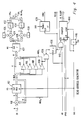
- FIGURE 1 is a block diagram showing video signal processing circuitry which includes a zoom feature incorporating the present invention.
- FIGURE 2 is a block diagram of field memory circuitry suitable for use in the video signal processing circuitry shown in FIGURE 1.
- FIGURE 3 is a timing diagram useful for describing tile operation of the field memory shown in FIGURE 2.
- FIGURE 4 is a block diagram of a read address generator suitable for use in the video signal processing circuitry shown in FIGURE 1.
- FIGURE 5 is a block diagram of a luminance/chrominance separator suitable for use in the video signal processing circuitry shown in FIGURE 1.
- FIGURE 6 is a block diagram of luminance signal vertical interpolation circuitry suitable for use in the video signal processing circuitry shown in FIGURE 1.
- FIGURE 7 is a block diagram of luminance signal horizontal interpolation circuitry suitable for use in the video signal processing circuitry shown in FIGURE 1.
- FIGURE 8 is a block diagram of chrominance signal vertical interpolation circuitry suitable for use in the video signal processing circuitry shown in FIGURE 1.
- FIGURE 9 is a block diagram of color difference signal horizontal interpolation circuitry suitable for use in the video signal processing circuitry shown in FIGURE 1.
- FIGURES 10A through 10D are timing diagrams useful for explaining the function of the zoom feature incorporated in the video signal processing circuitry shown in FIGURE 1.
- broad arrows represent busses for conveying multiple-bit parallel digital signals.
- Line arrows represent connections for conveying analog signals or single-bit digital signals.
- compensating delays may be required in certain of the signal paths.
- One skilled in the art of digital video signal processing circuit design would know where such delays would be needed in a particular system.
- the video signal processing circuitry shown in FIGURE 1 includes apparatus to perform a picture zoom function which allows video images to be magnified in real time using 128 magnification factors between one-to-one and two-to-one. Using a magnification factor of two-to-one, a portion of the original image occupying one-quarter of the display screen may be enlarged to occupy the entire screen.
- FIGURE 1 The following is a brief description of the various structural elements shown in FIGURE 1. This is followed by a more detailed description which refers to FIGURES 2-10.
- Digital sampled data composite video signals provided by an analog-to-digital converter (ADC) 14 are loaded into data storage elements of a field memory 16 that are addressed by write address values provided by a write address generator 20.
- the write address generator 20 is synchronized to a vertical synchronization signal VS.
- the memory 16 provides previously stored, sampled data composite video signals from data storage elements addressed by read address values provided by a read address generator 22.
- the read address generator 22 is synchronized to a delayed vertical synchronization signal DVS and is controlled by a vertical position signal VPOS provided by viewer controls 24.
- the signal VPOS conditions the memory 16 to provide only those lines of samples that lie within the portion of the image that is to be magnified.
- the sampled data composite video signal provided by the memory 16 is applied to luminance/chrominance separation circuitry 27.
- the circuitry 27 separates a luminance signal component, Y, and a combed chrominance signal component, C, from the sampled data composite video signal.
- the luminance signal, Y is expanded in the vertical direction by luminance signal vertical interpolation circuitry 28 using vertical interpolation factors ZRL.
- the factors ZRL are developed by the read address generator 22 from a magnification factor or zoom ratio, ZR, provided via the viewer controls 24.
- the vertically expanded luminance signal, provided by the interpolation circuitry 28, is applied to hanging dot correction circuitry 29, the output signal, Y, of which is expanded in the horizontal direction by luminance signal horizontal interpolation circuitry 30.
- the circuitry 30 interpolates only those samples occurring after a specified horizontal position, HPOS, provided via the viewer controls 24, to expand the lines of samples consistent with the zoom ratio ZR.
- the combed chrominance signal C provided by the separation circuitry 27 is expanded vertically by chrominance signal vertical interpolation circuitry 32, which also separates the chrominance signal into two quadrature phase related color difference signals, for example, I and Q.
- the vertically expanded color difference I ⁇ and Q ⁇ , provided by the circuitry 32 are expanded horizontally by color difference signal horizontal interpolation circuitry 34.
- the signals I ⁇ and Q ⁇ provided by the circuitry 34 and the signal Y ⁇ provided by the luminance signal horizontal interpolation circuitry 30 may, for example, be applied to conventional color difference and luminance signal processing circuitry (not shown) to produce a magnified image.
- a source of composite video signal 10 which may, for example, include the tuner, IF amplifier and video detector of a conventional color television receiver, provides a composite video signal to the ADC 14 and to sync separator and clock generator circuitry 12.
- the circuitry 12 which may be of conventional design, processes the composite video signals to produce a horizontal synchronization signal, HS, and the vertical synchronization signal, VS.
- the sync separator and clock generator 12 includes circuitry (not shown) which delays the signal VS by 128 horizontal line periods (128H) to produce the delayed vertical synchronization signal, DVS.
- the vertical deflection circuitry (not shown) of the video signal processing system which includes this circuitry, is responsive to the signal DVS for producing the magnified display.
- the circuitry 12 may also include a conventional burst-locked phase locked loop (not shown) which develops a clock signal, CK, having a frequency 4f c , which is four times the frequency, f c , of the color subcarrier component of the composite video signal.
- a delay of 128H between the signals VS and DVS allows any portion of a video image to be magnified by ratios ranging between one-to-one and two-to-one without producing an image that tears in the presence of interfield motion.
- the amount of delay between the signals VS and DVS may need to be programmable to avoid a torn image.
- the signal DVS would desirably be delayed by either 64 or 192 horizontal line periods depending on whether the portion of the image to be magnified is in the top half or the bottom half of the picture, respectively.
- This programmable delay may be realized, for example, by a programmable eight-bit counter (not shown) that is clocked by the signal HS.
- This counter is enabled by the signal VS and preset to 192 or 64 to produce delays of 64 and 192 horizontal line periods, respectively.
- the counter produces an output pulse on reaching a count value of 256.
- the ADC 14 which may, for example, be a conventional flash-type ADC, samples and digitizes the composite video signals applied to its input port at instants determined by the 4f c clock signal CK.
- the signal VIN provided by the ADC 14 is applied to the input port of the field memory 16.
- the field memory 16 appears to be a dual-port memory able to accept and provide continuous streams of eight-bit sample values (pixels) at a 4f c rate.
- the address values applied to the address input bus, ADDRESSA, of the memory 16 may be time division multiplexed to store a first stream of pixel data at one sequence of address values and simultaneously retrieve a second stream of pixel data using another sequence of address values.
- the field memory 16 is responsive to control signals provided by memory sequencing circuitry 18 as set forth below.
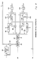
- FIGURE 2 is a block diagram of circuitry suitable for use as the field memory 16. This is a pipelined and interleaved memory system. Samples provided by the ADC 14 are stored either in memory cell array 218 or memory cell array 220. Each of the memory cell arrays 218 and 220 may include, for example, four 32K x 8 bit random access memory (RAM) integrated circuits (IC's) such as the HM65256AP manufactured by Hitachi. The memory IC's in each of the memory cell arrays 218 and 220 are configured to have mutually interconnected address and control input terminals but separate data input terminals.
- RAM random access memory
- the combination of the 4 IC's appears as a memory cell array having 32,768 addressable blocks where each block includes four data storage elements for holding, respectively, four eight-bit pixel values.
- the data read and data write operations to the memory cell arrays 218 and 220 are interleaved; while data is being written into the memory cell array 218 data is being read from the memory cell array 220 and vice-versa.
- this interleaving is achieved by dividing the field memory into two sections, A and B.
- the address and control signals applied to section B are delayed by four periods of the clock signal CK relative to the corresponding address and control signals applied to section A.
- a write operation using a second address value may be in progress in section A.
- a write operation using a third address value is performed on section A of the memory while the read operation using the second address value is performed on section B of the memory.
- the input buffer 212, memory cell array 218 and output buffer 230 are in section A and the input buffer 214, memory cell array 220 and output buffer 232 are in section B.
- FIGURE 2 The structure and operation of the field memory circuitry shown in FIGURE 2 is described using the timing diagrams shown in FIGURE 3, which illustrate the operation of the memory sequencing circuitry 18.
- the memory cell arrays 218 and 220 contain pixel data in blocks having addresses ADR1 and ADR1+1.
- Four pixel values of a block of data to be written into the memory cell arrays 218 and 220 have been applied to the shift register 210 at time T0, and the buffer registers 230 and 232 contain a block of pixel data read from the memory cell arrays 218 and 220 using the address value ADR1-1.
- the first operation is a memory read using address ADR1.
- the memory sequencing circuitry 18 pulses the signal LDO to transfer the block of pixel data held in the buffer registers 230 and 232, in parallel, into the output shift register 236. These pixel values are provided sequentially by the shift register 236 synchronous with the negative going edges of eight successive pulses of the signal CK.
- the address value ADR1 is applied to the ADDRESSA input port of the field memory 16.
- the chip enable signal CE A provided by the memory sequencing circuitry 18, is brought low, enabling the memory cell array 218.
- the signal OL A provided by the circuitry 18 is brought low, gating the input port of the buffer register 230 onto the bus DATAA.
- the memory sequencing circuitry 18 brings the output enable signal OE A low. This step in the memory read operation, enables the memory cell array 218 to apply the contents of the block of pixel data having the address ADR1 to the bus DATAA.
- the memory sequencing circuitry 18 brings the signal OL A high to latch the pixel data applied to the bus DATAA into the buffer register 230.
- the memory cell array 218 is disabled by bringing the signal CE A high and the memory read operation is complete.
- the address signal ADDRESSB, chip enable signal CE B, output enable signal OE B and output buffer load signal OL B are generated by delaying the corresponding signals ADDRESSA, CE A, OE A and OL A by four periods of the clock signal CK in the respective delay elements 222, 228, 226 and 234. Consequently, the memory read operation which read four pixel values from memory cell array 218 between times T0 and T1 is repeated on the memory cell array 220 between times T1 and T2.
- the eight pixel values, having the address ADR1, four from the memory cell array 218 and four from the memory cell array 220, are in the respective buffer registers 230 and 232.
- the signal LDO is pulsed by the circuitry 18 to transfer these eight pixel values, in parallel, to the shift register 236.
- the shift register 236 provides these pixel values sequentially for eight periods of the signal CK following time T2.
- a memory write operation using memory cell array 218 begins at time T1.
- the eighth input pixel value is shifted into the input shift register 210, immediately prior to the time T1.
- the memory sequencing circuitry 18 pulses the signal LDI to transfer the eight pixel values contained in the shift register 210 into the buffer registers 212 and 214.
- the memory sequencing circuitry begins to write the four pixel values held in the register 212 into the memory cell array 218.
- the address value ADR2, to be used to store these four pixel values, is applied to the address input port ADDRESSA of the field memory 16 at line T1.
- the memory sequencing circuitry 18 changes the input buffer enable signal IBE A and the write enable signal WE A to be logic zero.
- These signals respectively gate the values held in the input buffer 212 onto the bus DATAA and enable the memory cell array 218 to load the values on the bus DATAA into the addressed block.
- One-half of one period of the signal CK after time T1 the signal CE A is changed to logic zero by the circuitry 18, enabling the memory cell array 218 and, so, enabling the write operation to occur.
- the four pixel values held in the input buffer register 212 have stabilized in the block of the memory cell array 218 which has the address ADR2.
- One period of the clock signal CK after time T1 the circuitry 18 changes the signals IBE A and WE A to have values of logic one ending the memory write operation.
- Three and one-half clock periods after time T1 the circuitry 18 changes the chip enable signal CE A to a logic one, ending the memory write cycle.
- the signals IBE B and WE B are generated by delaying the corresponding signals IBE A and WE A by four periods of the signal CK in the respective delay elements 216 and 224. These signals, combined with the delayed address signal ADDRESSB and delayed chip enable signal CE B cause the memory write operation using the address value ADR2 to be repeated on the memory cell array 220 between time T2 and time T3. During this write operation, the four pixel values held in the buffer register 214 are transferred to the block of pixel storage cells in the memory cell array 220 that has the address value ADR2.
- a memory read operation is performed, using the memory cell array 218.
- four pixel values from a block of storage cells having the address ADR1+1 are read from the cell array 218 and loaded into the output buffer 230.
- This read operation is identical to the read operation performed between time T0 and time T1 and is not described in detail.
- a memory write operation In the time interval between times T3 and T4, a memory write operation, using an address value ADR2+1, writes the four pixel values, applied to the field memory 16 between times T2 and T3, into the memory cell array 218. Also between time T3 and time T4, four pixel values are read from the memory cell array 220 at the address ADR1+1 and are transferred to the output buffer register 232. These memory write and memory read operations are performed in the same manner as those described above and are not described in detail herein.
- the memory sequencing circuitry 18 is responsive to the clock signal CK to generate the signals IBE A, WE A, OE A, CE A, OL A, LDO and LDI.
- the circuitry 18 is reset at the beginning of each horizontal line of samples by the horizontal synchronization signal HS, provided by the sync separator and clock generator circuitry 12. This ensures that the first sample in any given line is stored in the field memory 16 on a block boundary.
- One skilled in the art of digital signal processing circuit design will be readily able to build suitable memory sequencing circuitry 18 from the description set forth above in reference to FIGURES 1, 2 and 3. Accordingly, the memory sequencing circuitry 18 is not described in detail herein.
- the address values applied to the field memory 16 have two parts, a line address, the eight most significant bits (MSB's), and a pixel block address, the seven least significant bits (LSB's).
- the line address values correspond to the 256 lines of video samples which may be written to or read from the memory 16 during one field interval.
- the pixel block address values correspond to the positions of successive blocks of eight pixel values on a horizontal line of the video image. The combination of a line address value and a pixel block address value points to a particular block of pixel storage cells in the field memory 16.
- the pixel block address signal, PADR, and a line address signal, WLADR, that is used to write data into the field memory 16, are generated by the write address generator 20.
- the generator 20 may include, for example, two counters (not shown).
- the first counter is reset by the vertical synchronization signal, VS, and incremented by the horizontal synchronization signal, HS.
- the count value provided by this first counter is the write-line address signal WLADR.
- the second counter is reset by the signal HS and incremented by a signal CK/8 having a frequency that is one-eighth the frequency of the signal CK.
- the signal CK/8 is generated by the memory sequencing circuitry 18 and may correspond, for example, to the signal LDO shown in FIGURE 3. This second counter produces the pixel block address signal which is used both for reading data from and writing data into the field memory 16.
- the write-line address signal WLADR and a read line address signal RLADR, provided by the read address generator 22, are applied to respective first and second input ports of a multiplexer 26.
- the multiplexer 26 is controlled by a signal CK/4, having a frequency that is one-fourth of the frequency of the signal CK.
- the signal CK/4 is provided by the memory sequencing circuitry 18 and is shown in the timing diagrams of FIGURE 3.
- the eight-bit signal provided by the multiplexer 26 forms the eight MSB's of the address signal, ADDRESSA, applied to the field memory 16.
- the pixel block address signal, PADR forms the seven LSB's of the signal ADDRESSA.
- the pixel block address portion of the signal ADDRESSA changes every eight periods of the clock signal CK to address successive blocks of pixel values in a horizontal line.
- the line address portion of the signal ADDRESSA changes every four periods of the signal CK, alternating between a line address value to be used to write data into the memory 16 and a line address value to be used to read data from the memory 16.
- FIGURE 4 is a block diagram of circuitry suitable for use as the read address generator 22.
- the generator 22 is responsive to the zoom ratio signal, ZR, and vertical position signal, VPOS, provided via the viewer controls 24, and to the horizontal synchronization signal, HS, and delayed vertical synchronization signal, DVS, to provide the line address signal RLADR used for the memory read operations.
- the read address generator 22 also provides a signal ZRL which contains the scale factors used by the vertical interpolation circuitry 28 and 32, a recirculate signal, RECIR, used by the luminance/chrominance separation circuitry 27, and a chrominance signal inversion signal, CINV, used by the chrominance signal vertical interpolation circuitry 32 as set forth below.
- the interpolation method used in this embodiment of the invention divides the space between any two successive lines in the original image into 255 potential interstitial line locations.
- the magnification factor used in this embodiment ranges from approximately 1 to 2, in steps of 1/256 (i.e. from 256/255 to 256/128). This relatively fine granularity in the magnification factor is desirable to produce the illusion of a continuous zoom when the magnification factor is changed. The fine granularity is more important for the spatial correctness of the entire image than for the proper interpolation of an individual line of samples or of an individual sample.
- the 255 potential interstitial line locations between any two successive lines may be grouped together into a smaller number of locations, for the purpose of interpolating an individual line of samples without seriously affecting the performance of the system.
- the interval between two successive lines of samples is divided into nine potential interpolation positions.
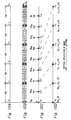
- FIGURES 10A through 10D are timing diagrams which illustrate how a line of samples is interpolated from a pair of successive lines to produce samples of the magnified image.
- FIGURE 10A illustrates that the interval between successive lines of samples may be divided into 256 parts.
- FIGURE 10B shows these 256 parts grouped together into nine interpolation positions.
- FIGURE 10C is an example of how interpolation is performed using a factor of 256/144 (i.e. 1.78).
- the position of individual lines of samples within the interpolation zones of FIGURE 10B are determined by repeatedly adding the value 144 to the value held by a modulo 256 accumulator.
- the first addition produces a value of 144, placing the first interpolated sample in a zone where 5/8 of the line of samples, L1, and 3/8 of the prior line of samples, L0, are summed to develop the interpolated line of samples, Z1.
- Adding 144 to the accumulator again yields a value of 32 (288 modulo 256).
- the line of samples, Z2 is formed by adding 1/8 of each sample in the line L2 to 7/8 of the corresponding sample in the line of samples L1.
- the lines of samples Z3 through Z8 are formed by repeatedly adding 144 to the accumulated value, modulo 256 and then using the relationship illustrated by the FIGURES 10B and 10C to determine which interpolation factors are to be used.
- FIGURE 10D illustrates how the picture is magnified in the vertical direction when the interpolated lines of samples Z0 through Z5 are displayed with the same timing as the original lines of samples.
- the zoom ratio value, ZR provided by the viewer controls 24 which, in this embodiment of the invention, may have a value between 128 and 255, is applied to one input port of an adder 410.
- the adder 410 sums the value ZR with the value held by an eight-bit register 412.
- the register 412 may include, for example, eight data type flip-flops configured as a parallel-input-parallel-output register.
- the register 412 is clocked by the horizontal synchronization signal, HS, to store the eight-bit value provided by the adder 410 once per horizontal line period.
- the register 412 is reset by the delayed vertical synchronization signal, DVS.
- the adder 410 and register 412 form a modulo 256 accumulator.
- the output value provided by the accumulator is the position of the interpolated line from among the 256 potential horizontal line positions between any two successive lines of the original image.
- the output values of the accumulator value are illustrated in FIGURE 10C.
- the four MSB's are coupled to the four inverters 414, 416, 418 and 420 which produce the one's complement of the value of the four MSB's.
- the one's complement is equal to (15-r) and is the numerator of the fraction (15-r)/16 which corresponds to the proportion of the contribution of the previous line to the interpolated value.
- the four MSB's of the value provided by the register 412 and the complemented four MSB's are concatenated as LSB's and MSB's, respectively, to produce values that are applied to a delay element 422.
- the delay element 422 is a synchronizing delay used to align the interpolation scale factors, ZRL, to the read line address signal, RLADR, and recirculate signal, RECIR.
- the values represented by the four LSB's of the signal provided by the delay element 422 are added to a value of one, provided by a digital value source 426 in an adder 424.
- Adding a one to the LSB's and dividing by two produces the value r1 which corresponds to the integer part of the eight-bit value provided by register 412 divided by thirty two, i.e. an integer value in the range 0-8.
- the value r1 is the numerator of the fraction r1/8 and, thus, is equal to 8K V where K V is the desired proportion of the contribution of the current line.
- the four MSB's of the signal provided by the delay element 422 (the ones-complement values) are added to a value of one provided by a digital value source 430 in an adder 428.
- the signal provided by the adder 428 is divided by two in the divider 434 to produce a signal 8(1-K) V which represents the second vertical interpolation factor, multiplied by eight.
- the signal 8(1-K) V is used by the vertical interpolation circuitry 28 and 32 to develop the interpolated lines of samples which represent the magnified image.
- the signal 8K V is the four LSB's, and the signal 8(1-K) V is the four MSB's of the signal ZRL.
- FIGURE 10B illustrates how the factors 8K V and 8(1-K) V are mapped onto the 256 interstitial line positions between successive lines of samples.
- a signal, MSB0, representing the most significant bit of the value provided by the adder 410 and a signal MSB1, representing the inverted most significant bit of the value provided by the register 412 are combined in a NAND gate 436 to produce a signal, which, when delayed by one horizontal line period by the delay element 438, becomes the recirculate signal RECIR.
- the signal provided by the NAND gate 436 has a logic zero value only when the most significant bit of the value provided by the register 412 is a zero and the most significant bit of the value provided by the adder 410 is a one. These values indicate that two successive interpolated lines of samples are to be interpolated from the same two lines of samples from the original image.
- the signal RECIR may be obtained by inverting an overflow output signal (not shown) provided by the adder 410 and delaying this inverted signal by two periods of the horizontal line synchronizing signal, HS.
- the signal RECIR is applied to the clock input port of a toggle-type flip-flop 439.
- the flip-flop 439 which may be, for example, a conventional J-K flip-flop having a value of logic one applied to both its J and K input terminals, changes its output state from a logic one to a logic zero and vice-versa each time a pulse is applied to its clock input terminal, CLK.
- the flip-flop 439 is reset to have a logic zero output state by the delayed vertical synchronization signal DVS.
- the signal CINV changes state each time that two successive lines of interpolated signal are developed from one pair of lines of the original signal.
- the signal CINV controls the inversion of the chrominance samples developed by the chrominance signal vertical interpolation circuitry described below. This signal enables the chrominance signals developed by the circuitry 32 to be properly demodulated into the I and Q color difference signals by conventional chrominance signal demodulation circuitry.
- the signal RECIR is applied to the luminance/chrominance separation circuitry 27 and to one input terminal of an AND gate 442. Another input terminal of the AND gate 442 is coupled to receive the horizontal synchronization signal HS. The signal provided by the AND gate 442 is applied to the clock input terminal of a counter 444 which produces the signal RLADR.
- the counter 444 increments its value once per horizontal line period unless the lines of samples used to generate the next interpolated line are the same as those that were used to generate the prior interpolated line.
- the counter 444 is cleared by the delayed vertical sync signal, DVS.
- the vertical position value VPOS is loaded as an initial value into the counter 444 by a delayed version of the signal DVS provided by the delay element 446.
- the counter 444 is cleared and preset by the signal DVS to ensure that the lines of samples read from the field memory 16 during one field interval are all from the same field of the input video signal. For example, when a magnification factor of 256/128 (2) is used, memory write operations occur at twice the rate of the memory read operations. In the present embodiment of the invention, the field memory 16 holds 256 lines of samples. In this example, the image to be expanded occupies a portion of the lower one-half of the original image. Since the memory read operation is synchronized to the DVS, the first line to be expanded, line number 128 of the original signal, is read from the memory one horizontal line period after it was written into the memory.
- the lines of samples displayed at the top of this expanded image would be from the previous field relative to the lines of samples displayed at the bottom of the image. Conversely, if the signal DVS were delayed by more than 128 horizontal line periods and a portion of the top half of the original image were magnified by a factor of 2, the lines of samples displayed at the bottom of the expanded image would be from the subsequent field relative to the lines of samples displayed at the top of the image. As set forth above, displaying samples from a single field is desirable to avoid a "tearing" of the image which may occur because of interfield motion. As set forth above, the vertical deflection circuitry (not shown) of the television receiver which produces the magnified display is controlled by the signal DVS.
- FIGURE 5 is a block diagram of exemplary luminance/chrominance separation circuitry.
- the lines of samples of the video signal, VOUT, provided by the field memory 16 are applied to one input port of a multiplexer 510, the output port of which is coupled to a one horizontal line period (1H) delay element 512.
- the output signal provided by the 1H delay element 512 is applied to a second input port of the multiplexer 510.
- the control input terminal of the multiplexer 510 is coupled to receive the signal RECIR.
- the multiplexer 510 is conditioned to pass the signal VOUT to the 1H delay element 512.
- the multiplexer 510 is conditioned to recirculate the samples provided by the 1H delay element 512 back to the input terminal of the delay element.
- FIGURE 5 implements a conventional 1H comb filter.
- Corresponding samples from a delayed line of samples and from an undelayed line of samples are summed in an adder 514 to provide a luminance signal, Y.
- the delayed samples are subtracted from the undelayed samples to produce a comb filtered chrominance signal, C, which includes chrominance signal components and relatively low frequency vertical detail signal components.
- the signal RECIR conditions the comb filter to use samples from the same pair of lines to generate the signals Y and C when two successive lines of the expanded video signal are to be interpolated from one pair of lines of the original video signal.
- the luminance signal, Y provided by the luminance/chrominance separation circuitry 27 is applied to the luminance signal vertical interpolator 28.
- FIGURE 6 is a block diagram of circuitry suitable for use as the interpolator 28.
- the luminance signal Y is applied to a delay element 610.
- the delay element 610 compensates the luminance signal Y for processing delays through the chrominance signal vertical interpolator circuitry 32 (described below) that develops the vertical detail signal, VDET.
- An adder 612 and a subtracter 618 respectively add the vertical detail signal, VDET, to and subtract the signal VDET from the luminance signal provided by the delay element 610.
- the signals developed by the adder 612 and subtracter 618 approximate the luminance signal components of two successive lines of the original video signal.
- the samples produced by the adder 612 which approximate the luminance samples from a current line of video signal, are multiplied, in a multiplier 614, by the interpolation scale factor 8K V provided by the read address generator 22 via the bus ZRL.
- the output signals of the multiplier 614 are applied to one input port of an adder 616.
- the luminance signal provided by the subtracter 618 which approximates luminance samples from the previous line of video signal, is scaled by the interpolation scale factor 8(1-K) in a multiplier 620.
- the output signal of the multiplier 620 is applied to a second input port of the adder 616.
- the output signal of the adder 616 is divided by 8 in the circuitry 622 to produce the vertically interpolated luminance signal.
- the signal developed by the luminance signal vertical interpolation circuitry 28 is applied to hanging dot correction circuitry 29.
- the circuitry 29 which may, for example, be the same as that described in U.S. Patent No. 4,636,842 entitled “Comb Filter 'Hanging Dot' Eliminator", removes spurious chrominance signal components from the vertically interpolated luminance signal based on the magnitude of the vertical detail signal VDET.
- the circuitry 29 is described in the above referenced patent and, so, is not described herein.
- FIGURE 7 is a block diagram showing circuitry suitable for use as the luminance signal horizontal interpolator 30.
- the circuitry shown in FIGURE 7 is divided into two parts.
- the circuitry which processes the signal Y ⁇ to produce the signal Y ⁇ is inside the dashed-line box, identified by the reference number 710.
- the remainder of the circuitry shown in FIGURE 7 controls the circuitry 710 and also controls the color difference signal horizontal interpolation circuitry 34 as set forth below in reference to FIGURE 9.
- the vertically interpolated luminance signal, Y ⁇ is applied to the input port of a demultiplexer 712.
- the demultiplexer 712 applies the lines of samples of the signal Y ⁇ alternately to 1H random access memories 714 and 716.
- the signal controlling the demultiplexer 712 is generated by halving the frequency of the horizontal synchronization signal, HS, in the frequency dividing circuitry 732.
- the output ports of the memories 714 and 716 are coupled to respective first and second input ports of a multiplexer 718.
- the multiplexer 718 is controlled by the signal generated by the frequency divider 732 to provide samples from memory 714 when the demultiplexer 712 is conditioned to apply samples to the memory 716 and to provide samples from memory 716 when the demultiplexer 712 is conditioned to apply samples to the memory 714.
- the samples provided by the multiplexer 718 are applied to a delay element 720 which is controlled by a gated clock signal provided by an AND gate 764 as set forth below.
- the delay element 720 provides samples to a multiplier 724 and to a delay element 722.
- the delay element 722 is also clocked by the gated clock signal provided by the AND gate 764.
- the samples provided by the delay element 722 are applied to a multiplier 726.
- the multipliers 724 and 726 which may, for example, be conventional 8-bit x 8-bit multipliers, scale the sample values provided by the respective delay elements 720 and 722 by interpolation factors 8K H and 8(1-K) H provided by dividing circuits 776 and 774, respectively.
- the scaled samples provided by the multiplying circuits 724 and 726 are summed in an adder 728 and divided by eight in sample value dividing circuitry 730 to produce samples representing the interpolated signal Y ⁇ .
- the circuitry that controls the interpolating circuitry 710 also develops the address values used to access the memories 714 and 716 and the interpolation scale factors used by the multipliers 724 and 726.
- Each of the 1H memories 714 and 716 is a random access memory. Address values used to access the memory 714 are provided by a multiplexer 736 while address values used to access the memory 716 are provided by the multiplexer 734. Each of the multiplexers 734 and 736 are coupled to receive read address values at respective first input ports from a read address counter 738 and to receive write address values at respective second input ports from a write address counter 740. The multiplexers 734 and 736 are conditioned by the signal provided by the frequency divider 732 to apply the write address values to the memory 714 or 716, whichever one is coupled to receive video samples from the demultiplexer 712, and to apply read address values to the other one of the memories 714 and 716.
- the write address counter 740 may be, for example, a ten-bit counter which is clocked by the 4f c signal CK and which is reset by the horizontal synchronization signal, HS.
- the read address counter 738 may also be a ten-bit counter which is clocked by a gated version of the signal CK provided by an AND gate 744 as set forth below.
- the counter 738 used in this embodiment of the invention, is a presettable counter.
- the horizontal position value, HPOS provided via the viewer controls 24 is applied to the counter 738 as the preset value. This value is loaded into the counter 738 coincident with a pulse of the horizontal synchronization signal, HS, delayed by one period of the signal CK via the delay element 742.
- the gated clock signal provided by the AND gate 744 is the logical AND of the clock signal CK and a signal ADHOLD provided by a NAND gate 746.
- the signal ADHOLD inhibits the read address counter 738 from incrementing when two successive interpolated samples are to be developed from a single pair of sample values of the signal Y ⁇ .
- the circuitry which generates the signal ADHOLD also generates the horizontal interpolation scale factors used to develop the signal Y ⁇ .
- the zoom ratio signal, ZR is applied to one input port of an adder 758.
- the output port of the adder 758 is coupled to the input port of an eight-bit register 756 which is clocked by the signal CK.
- the output port of the register 756 is coupled to a second input port the adder 758.
- the four MSB's of the value provided by the register 256 are applied to the input port of a delay element 760 both directly and via the respective inverters 748, 750, 752 and 754.
- the signal applied to the delay element 760 is an eight-bit signal.
- the four-bits provided by the inverters 748 through 754 are the four MSB's of this eight-bit signal and the four-bits provided by register 756 directly form the four LSB's of the signal.
- the signal HMSB0, the most significant bit of the signal provided by the register 756, and the signal HMSB1, the most significant bit of the signal provided by the delay element 760, are applied to the NAND gate 746 to generate the signal ADHOLD.
- the signal ADHOLD has a value of logic zero only when the signal HMSB0 and HMSB1 are both logic one. This occurs when the most significant bit of the value provided by the register 756 is a logic zero during one period of the signal CK and is a logic one during the next successive period of the signal CK. In this instance, two successive samples of the interpolated signal Y ⁇ are developed from one pair of samples of the signal Y ⁇ .
- the signal ADHOLD may be generated by inverting an overflow output signal (not shown) of the adder 758 and delaying this inverted output signal by two periods of the signal CK.
- the signal ADHOLD is delayed by one period of the signal CK, via the delay element 762, and applied to the input terminal of the AND gate 764.
- Another input terminal of the AND gate 764 is coupled to receive the clock signal CK.
- the signal provided by the AND gate 764 cycles successive samples of the signal Y ⁇ through the delay elements 720 and 722 for use by the interpolating multipliers 724 and 726.
- the clock signal applied to the delay elements 720 and 722 is disabled for one period of the signal CK.
- the samples provided by the delay elements 720 and 722 are processed by the multipliers 724 and 726 as set forth above.
- the values represented by the four LSB's of the signal provided by the delay elements 760 are added, in an adder 770, to a value of one supplied by a digital value source 772.
- the signal developed by the adder 770 is applied to a divider 776 which divides it by two to produce the horizontal interpolation factor 8K H . This factor is applied to the interpolating multiplier 724.
- the values represented by the four MSB's of the signal provided by the delay element 760 are added, in an adder 766, to a value of one provided by a digital value source 768.
- the values developed by the adder 766 are divided by two in the dividing circuitry 774 to produce the horizontal interpolation factor 8(1-K) H . This factor is applied to the interpolating multiplier 726.
- the operation of the interpolating multipliers 724 and 726 is set forth above.
- FIGURE 8 is a block diagram of circuitry suitable for use as the interpolator 32.
- the sampled data combed chrominance signal, C, provided by the separation circuitry 27 is applied to a vertical detail low-pass filter 810.
- the filter 810 which may, for example, have a frequency characteristic pass band from O H z to 2 MHz passes the relatively low frequency luminance vertical detail components of the signal C to the substantial exclusion of any chrominance signal components.
- the filter 810 provides the vertical detail signal, VDET, which is used by the luminance signal vertical interpolation circuitry 28 as set forth above.
- the signal VDET is subtracted from the signal C by the subtracter 812 to produce samples representing the chrominance band signal components of the comb filtered chrominance signal C.
- the signals developed by the subtracter 812 are applied to selective chrominance signal inverting circuitry 813.
- the circuitry 813 is controlled by the chrominance inversion signal, CINV, developed by the read address generator 22 as set forth above.
- the circuitry 813 acts to preserve the phase relationship between the clock signal CK and the I and Q phases of the vertically interpolated chrominance signal when successive lines of interpolated samples are derived from one pair of lines of the signal C.
- the phase corrected chrominance samples provided by the inverting circuitry 813 are applied to a chrominance signal demodulator 814.
- the demodulator 814 processes these samples to develop the two color difference signals I and Q.
- the signal I is applied to a 1H delay element 816 and to a multiplier 818.
- the 1H delayed I signal provided by the delay element 816 is applied to a multiplier 820.
- the multiplexers 818 and 820 which may be, for example, conventional 8 x 8 bit multipliers, scale the respective undelayed and delayed I signal sample values by the respective interpolation scale factors 8K V and 8(1-K) V provided by the read address generator circuitry 22 as set forth above.
- the scaled samples provided by the multipliers 818 and 820 are summed in an adder 822.
- the signal provided by the adder 822 is divided by eight in the dividing circuitry 824 to produce vertically interpolated lines of samples of a signal I ⁇ for application to the color difference signal horizontal interpolation circuitry 34.
- the Q color difference signals provided by the chrominance signal demodulator 814 are applied to circuitry which includes a 1H delay element 826, interpolating multipliers 828 and 830, an adder 832 and a sample value divider 834. This circuitry develops the vertically interpolated color difference signal, Q ⁇ .
- the Q signal vertical interpolation circuitry performs identically to the I signal vertical interpolation circuitry described above; consequently, it is not described in detail.
- samples of a color difference signal from one line of the input video signal may be simultaneously provided to both of the interpolating multipliers 818 and 820.
- the I ⁇ output signal of the interpolator 32 is the uninterpolated I signal. Due to the relatively low sensitivity of the eye to changes in color, artifacts resulting from the use of these uninterpolated samples are not objectionable.
- the chrominance signal vertical interpolator circuitry 32 may be reduced to the vertical detail filter 810, subtracter 812, chrominance signal inverter 813 and chrominance signal demodulator 814; completely eliminating the 1H delay elements 816 and 826, the multipliers 818, 820, 826 and 828, the adders 822 and 832 and the sample value dividing circuits 824 and 834, without seriously impairing the quality of the reproduced image.
- FIGURE 9 is a block diagram showing circuitry suitable for use as the horizontal interpolation circuitry 34.
- the circuitry 950 used to develop the interpolated Q color difference signal is identical to the circuitry used to develop the interpolated I color difference signal and, so, the circuitry 950 is shown as a single block.
- the circuitry, 910, used to develop the interpolated I color difference signal is, itself, identical to the circuitry 710 used to develop the horizontally interpolated luminance signals, accordingly, the circuitry 910 and the circuitry 950 are not described in detail.
- the horizontally and vertically interpolated color difference signals, I ⁇ and Q ⁇ , provided by the respective circuits 910 and 950 may be applied, for example, to conventional color difference signal processing circuits (not shown) and combined with the signal Y ⁇ to produce a magnified image.
Landscapes
- Engineering & Computer Science (AREA)
- Multimedia (AREA)
- Signal Processing (AREA)
- Physics & Mathematics (AREA)
- General Physics & Mathematics (AREA)
- Theoretical Computer Science (AREA)
- Studio Circuits (AREA)
- Television Systems (AREA)
- Processing Of Color Television Signals (AREA)
- Television Signal Processing For Recording (AREA)
Description
- The present invention relates to a memory system which may be used for instance in a television picture magnification system.
- Recent progress in digital video signal processing has led to the proposal of several television picture magnification systems. One of these systems, set forth in U.S. Patent No. US-A-4,302,776 entitled "Digital Still Picture Storage System With Size Change Facility" uses a real time frame store to capture one frame of video information. This information is read from the frame store using a much slower non-real-time data rate and applied to circuitry which generates a signal representing a magnified or reduced size frozen image.
- A second system, set forth in U.S. Patent No. US-A-4,633,503 entitled "Video Zoom Processor" is able to expand video signals in real time to produce a magnified image. In this system, input video samples are written into one of two field memories while samples to be processed are read from the other memory.
- A third picture magnifying system, set forth in U.S. Patent No. US-A-4,282,546 entitled "Television Image Size Altering Apparatus" develops a time-expanded video signal by storing sampled data video signals into a memory at a standard video rate, and then reading the samples at a reduced rate. If this memory were a single field memory, able to accept and provide continuous streams of sample values, the image produced by the system may be distorted. This distortion occurs because samples are read from the memory at a lower rate than that used to write samples into the memory. Under these conditions, samples representing one field on the expanded image may be read from the memory while samples representing portions of two different fields are written into the memory. In this instance, the resultant magnified picture may include information from two successive fields, causing distortion when the image includes interfield motion. This distortion may be described as a "tearing" of the image on the boundary where samples from the two different fields are displayed.
- In a fourth system disclosed in EP-A-0220880, a time base expanding signal interpolator arrangement is described. This arrangement uses a modified sequence of sample position memory addresses containing address repetitions and includes residual signals corresponding to subdivisions of the intervals between successive different addresses in the modified sequence.
- A fifth system for enlarging or reducing two-dimensional images is disclosed in EP-A-0093429. In such disclosed arrangement, an original matrix of image elements is transformed into a scale converted matrix, using coordinate and saturation calculations, with account taken of the periodicity of the positional relation between the original and scale converted matrices.
- The present invention is embodied in circuitry which produces, from a source of sampled data video signal, a time-expansion video signal occurring as a sequence of field intervals. The circuitry includes a memory having a sufficient number of sample storage cells to hold M samples. A memory write address signal generator conditions the memory to store, during a first time interval, M samples representing one field of said source video signal. A read address signal generator conditions the memory to provide N consecutive stored samples from one field of the source data video during a second time interval, where integer N is less than integer M. A sample processor is responsive to the N provided samples for interpolating the N samples to generate M samples representing one field of a time-expanded video signal having a field interval substantially equal to the field interval of the source data video signal. The first and second time intervals each span an amount of time approximately equal to one field interval of the source data video signal and the beginning of the second time interval is delayed by an amount of time less than one field interval of the source data video signal relative to the beginning of the first time interval.
- FIGURE 1 is a block diagram showing video signal processing circuitry which includes a zoom feature incorporating the present invention.
- FIGURE 2 is a block diagram of field memory circuitry suitable for use in the video signal processing circuitry shown in FIGURE 1.
- FIGURE 3 is a timing diagram useful for describing tile operation of the field memory shown in FIGURE 2.
- FIGURE 4 is a block diagram of a read address generator suitable for use in the video signal processing circuitry shown in FIGURE 1.
- FIGURE 5 is a block diagram of a luminance/chrominance separator suitable for use in the video signal processing circuitry shown in FIGURE 1.
- FIGURE 6 is a block diagram of luminance signal vertical interpolation circuitry suitable for use in the video signal processing circuitry shown in FIGURE 1.
- FIGURE 7 is a block diagram of luminance signal horizontal interpolation circuitry suitable for use in the video signal processing circuitry shown in FIGURE 1.
- FIGURE 8 is a block diagram of chrominance signal vertical interpolation circuitry suitable for use in the video signal processing circuitry shown in FIGURE 1.
- FIGURE 9 is a block diagram of color difference signal horizontal interpolation circuitry suitable for use in the video signal processing circuitry shown in FIGURE 1.
- FIGURES 10A through 10D are timing diagrams useful for explaining the function of the zoom feature incorporated in the video signal processing circuitry shown in FIGURE 1.
- In the drawings, broad arrows represent busses for conveying multiple-bit parallel digital signals. Line arrows represent connections for conveying analog signals or single-bit digital signals. Depending on the processing speed of the devices used, compensating delays may be required in certain of the signal paths. One skilled in the art of digital video signal processing circuit design would know where such delays would be needed in a particular system.
- The video signal processing circuitry shown in FIGURE 1 includes apparatus to perform a picture zoom function which allows video images to be magnified in real time using 128 magnification factors between one-to-one and two-to-one. Using a magnification factor of two-to-one, a portion of the original image occupying one-quarter of the display screen may be enlarged to occupy the entire screen.
- The following is a brief description of the various structural elements shown in FIGURE 1. This is followed by a more detailed description which refers to FIGURES 2-10.
- Digital sampled data composite video signals provided by an analog-to-digital converter (ADC) 14 are loaded into data storage elements of a
field memory 16 that are addressed by write address values provided by awrite address generator 20. Thewrite address generator 20 is synchronized to a vertical synchronization signal VS. Thememory 16 provides previously stored, sampled data composite video signals from data storage elements addressed by read address values provided by aread address generator 22. Theread address generator 22 is synchronized to a delayed vertical synchronization signal DVS and is controlled by a vertical position signal VPOS provided byviewer controls 24. The signal VPOS conditions thememory 16 to provide only those lines of samples that lie within the portion of the image that is to be magnified. The sampled data composite video signal provided by thememory 16 is applied to luminance/chrominance separation circuitry 27. Thecircuitry 27 separates a luminance signal component, Y, and a combed chrominance signal component, C, from the sampled data composite video signal. The luminance signal, Y, is expanded in the vertical direction by luminance signalvertical interpolation circuitry 28 using vertical interpolation factors ZRL. The factors ZRL are developed by theread address generator 22 from a magnification factor or zoom ratio, ZR, provided via theviewer controls 24. The vertically expanded luminance signal, provided by theinterpolation circuitry 28, is applied to hangingdot correction circuitry 29, the output signal, Y, of which is expanded in the horizontal direction by luminance signalhorizontal interpolation circuitry 30. Thecircuitry 30 interpolates only those samples occurring after a specified horizontal position, HPOS, provided via theviewer controls 24, to expand the lines of samples consistent with the zoom ratio ZR. - The combed chrominance signal C provided by the
separation circuitry 27 is expanded vertically by chrominance signalvertical interpolation circuitry 32, which also separates the chrominance signal into two quadrature phase related color difference signals, for example, I and Q. The vertically expanded color difference Iʹ and Qʹ, provided by thecircuitry 32 are expanded horizontally by color difference signalhorizontal interpolation circuitry 34. The signals Iʺ and Qʺ provided by thecircuitry 34 and the signal Yʺ provided by the luminance signalhorizontal interpolation circuitry 30 may, for example, be applied to conventional color difference and luminance signal processing circuitry (not shown) to produce a magnified image. - The following is a more detailed description of the video signal processing circuitry shown in FIGURE 1. A source of
composite video signal 10, which may, for example, include the tuner, IF amplifier and video detector of a conventional color television receiver, provides a composite video signal to theADC 14 and to sync separator and clock generator circuitry 12. The circuitry 12, which may be of conventional design, processes the composite video signals to produce a horizontal synchronization signal, HS, and the vertical synchronization signal, VS. In addition, the sync separator and clock generator 12 includes circuitry (not shown) which delays the signal VS by 128 horizontal line periods (128H) to produce the delayed vertical synchronization signal, DVS. The vertical deflection circuitry (not shown) of the video signal processing system which includes this circuitry, is responsive to the signal DVS for producing the magnified display. The circuitry 12 may also include a conventional burst-locked phase locked loop (not shown) which develops a clock signal, CK, having a frequency 4fc, which is four times the frequency, fc, of the color subcarrier component of the composite video signal. - As set forth below, a delay of 128H between the signals VS and DVS allows any portion of a video image to be magnified by ratios ranging between one-to-one and two-to-one without producing an image that tears in the presence of interfield motion. For magnification ratios larger than two-to-one, the amount of delay between the signals VS and DVS may need to be programmable to avoid a torn image. For example, if a magnification ratio of four-to-one were used, the signal DVS would desirably be delayed by either 64 or 192 horizontal line periods depending on whether the portion of the image to be magnified is in the top half or the bottom half of the picture, respectively. This programmable delay may be realized, for example, by a programmable eight-bit counter (not shown) that is clocked by the signal HS. This counter is enabled by the signal VS and preset to 192 or 64 to produce delays of 64 and 192 horizontal line periods, respectively. The counter produces an output pulse on reaching a count value of 256.
- The
ADC 14, which may, for example, be a conventional flash-type ADC, samples and digitizes the composite video signals applied to its input port at instants determined by the 4fc clock signal CK. The signal VIN provided by theADC 14 is applied to the input port of thefield memory 16. - Externally, the
field memory 16 appears to be a dual-port memory able to accept and provide continuous streams of eight-bit sample values (pixels) at a 4fc rate. The address values applied to the address input bus, ADDRESSA, of thememory 16 may be time division multiplexed to store a first stream of pixel data at one sequence of address values and simultaneously retrieve a second stream of pixel data using another sequence of address values. Thefield memory 16 is responsive to control signals provided bymemory sequencing circuitry 18 as set forth below. - FIGURE 2 is a block diagram of circuitry suitable for use as the
field memory 16. This is a pipelined and interleaved memory system. Samples provided by theADC 14 are stored either inmemory cell array 218 ormemory cell array 220. Each of thememory cell arrays memory cell arrays memory cell arrays memory cell array 218 data is being read from thememory cell array 220 and vice-versa. In general, this interleaving is achieved by dividing the field memory into two sections, A and B. The address and control signals applied to section B are delayed by four periods of the clock signal CK relative to the corresponding address and control signals applied to section A. Consequently, while a read operation, using a first address value is in progress in section B of the memory, a write operation using a second address value may be in progress in section A. Four clock periods later, a write operation using a third address value is performed on section A of the memory while the read operation using the second address value is performed on section B of the memory. In the system shown in FIGURE 2, theinput buffer 212,memory cell array 218 andoutput buffer 230 are in section A and theinput buffer 214,memory cell array 220 andoutput buffer 232 are in section B. - The structure and operation of the field memory circuitry shown in FIGURE 2 is described using the timing diagrams shown in FIGURE 3, which illustrate the operation of the
memory sequencing circuitry 18. In the example shown in FIGURE 3, thememory cell arrays memory cell arrays shift register 210 at time T₀, and the buffer registers 230 and 232 contain a block of pixel data read from thememory cell arrays - The first operation is a memory read using address ADR1. At time T₀, the
memory sequencing circuitry 18 pulses the signal LDO to transfer the block of pixel data held in the buffer registers 230 and 232, in parallel, into theoutput shift register 236. These pixel values are provided sequentially by theshift register 236 synchronous with the negative going edges of eight successive pulses of the signal CK. Also at time T₀, the address value ADR1 is applied to the ADDRESSA input port of thefield memory 16. One-half of one period of the clock signal CK following time T₀, the chip enable signalCE A provided by thememory sequencing circuitry 18, is brought low, enabling thememory cell array 218. One clock period after time T₀, the signalOL A, provided by thecircuitry 18 is brought low, gating the input port of thebuffer register 230 onto the bus DATAA. At a time one and one-half periods of the signal CK after time T₀, thememory sequencing circuitry 18 brings the output enable signalOE A low. This step in the memory read operation, enables thememory cell array 218 to apply the contents of the block of pixel data having the address ADR1 to the bus DATAA. Three clock periods after T₀, thememory sequencing circuitry 18 brings the signalOL A high to latch the pixel data applied to the bus DATAA into thebuffer register 230. Three and one-half clock cycles after time T₀, thememory cell array 218 is disabled by bringing the signalCE A high and the memory read operation is complete. - The address signal ADDRESSB, chip enable signal
CE B, output enable signalOE B and output buffer load signalOL B are generated by delaying the corresponding signals ADDRESSA,CE A,OE A andOL A by four periods of the clock signal CK in therespective delay elements memory cell array 218 between times T₀ and T₁ is repeated on thememory cell array 220 between times T₁ and T₂. At time T₂, the eight pixel values, having the address ADR1, four from thememory cell array 218 and four from thememory cell array 220, are in the respective buffer registers 230 and 232. At time T₂, the signal LDO is pulsed by thecircuitry 18 to transfer these eight pixel values, in parallel, to theshift register 236. Theshift register 236 provides these pixel values sequentially for eight periods of the signal CK following time T₂. - A memory write operation using
memory cell array 218 begins at time T₁. The eighth input pixel value is shifted into theinput shift register 210, immediately prior to the time T₁. At time T₁, thememory sequencing circuitry 18 pulses the signal LDI to transfer the eight pixel values contained in theshift register 210 into the buffer registers 212 and 214. At time T₁, the memory sequencing circuitry begins to write the four pixel values held in theregister 212 into thememory cell array 218. The address value ADR2, to be used to store these four pixel values, is applied to the address input port ADDRESSA of thefield memory 16 at line T₁. Also at time T₁, thememory sequencing circuitry 18 changes the input buffer enable signalIBE A and the write enable signalWE A to be logic zero. These signals respectively gate the values held in theinput buffer 212 onto the bus DATAA and enable thememory cell array 218 to load the values on the bus DATAA into the addressed block. One-half of one period of the signal CK after time T₁, the signalCE A is changed to logic zero by thecircuitry 18, enabling thememory cell array 218 and, so, enabling the write operation to occur. At the time TW₀, the four pixel values held in theinput buffer register 212 have stabilized in the block of thememory cell array 218 which has the address ADR2. One period of the clock signal CK after time T₁, thecircuitry 18 changes the signalsIBE A andWE A to have values of logic one ending the memory write operation. Three and one-half clock periods after time T₁, thecircuitry 18 changes the chip enable signalCE A to a logic one, ending the memory write cycle. - The signals
IBE B andWE B are generated by delaying the corresponding signalsIBE A andWE A by four periods of the signal CK in therespective delay elements CE B cause the memory write operation using the address value ADR2 to be repeated on thememory cell array 220 between time T₂ and time T₃. During this write operation, the four pixel values held in thebuffer register 214 are transferred to the block of pixel storage cells in thememory cell array 220 that has the address value ADR2. - Coincident with this second write operation using the
memory cell array 220, a memory read operation is performed, using thememory cell array 218. During the time interval between time T₂ and time T₃, four pixel values from a block of storage cells having the address ADR1+1 are read from thecell array 218 and loaded into theoutput buffer 230. This read operation is identical to the read operation performed between time T₀ and time T₁ and is not described in detail. - In the time interval between times T₃ and T₄, a memory write operation, using an address
value ADR2+ 1, writes the four pixel values, applied to thefield memory 16 between times T₂ and T₃, into thememory cell array 218. Also between time T₃ and time T₄, four pixel values are read from thememory cell array 220 at the address ADR1+1 and are transferred to theoutput buffer register 232. These memory write and memory read operations are performed in the same manner as those described above and are not described in detail herein. - The
memory sequencing circuitry 18 is responsive to the clock signal CK to generate the signalsIBE A,WE A,OE A,CE A,OL A, LDO and LDI. Thecircuitry 18 is reset at the beginning of each horizontal line of samples by the horizontal synchronization signal HS, provided by the sync separator and clock generator circuitry 12. This ensures that the first sample in any given line is stored in thefield memory 16 on a block boundary. One skilled in the art of digital signal processing circuit design will be readily able to build suitablememory sequencing circuitry 18 from the description set forth above in reference to FIGURES 1, 2 and 3. Accordingly, thememory sequencing circuitry 18 is not described in detail herein. - The address values applied to the
field memory 16 have two parts, a line address, the eight most significant bits (MSB's), and a pixel block address, the seven least significant bits (LSB's). The line address values correspond to the 256 lines of video samples which may be written to or read from thememory 16 during one field interval. The pixel block address values correspond to the positions of successive blocks of eight pixel values on a horizontal line of the video image. The combination of a line address value and a pixel block address value points to a particular block of pixel storage cells in thefield memory 16. - The pixel block address signal, PADR, and a line address signal, WLADR, that is used to write data into the
field memory 16, are generated by thewrite address generator 20. Thegenerator 20 may include, for example, two counters (not shown). The first counter is reset by the vertical synchronization signal, VS, and incremented by the horizontal synchronization signal, HS. The count value provided by this first counter is the write-line address signal WLADR. The second counter is reset by the signal HS and incremented by a signal CK/8 having a frequency that is one-eighth the frequency of the signal CK. The signal CK/8 is generated by thememory sequencing circuitry 18 and may correspond, for example, to the signal LDO shown in FIGURE 3. This second counter produces the pixel block address signal which is used both for reading data from and writing data into thefield memory 16. - The write-line address signal WLADR and a read line address signal RLADR, provided by the read
address generator 22, are applied to respective first and second input ports of amultiplexer 26. Themultiplexer 26 is controlled by a signal CK/4, having a frequency that is one-fourth of the frequency of the signal CK. The signal CK/4 is provided by thememory sequencing circuitry 18 and is shown in the timing diagrams of FIGURE 3. The eight-bit signal provided by themultiplexer 26 forms the eight MSB's of the address signal, ADDRESSA, applied to thefield memory 16. The pixel block address signal, PADR, forms the seven LSB's of the signal ADDRESSA. In the present embodiment of the invention, the pixel block address portion of the signal ADDRESSA changes every eight periods of the clock signal CK to address successive blocks of pixel values in a horizontal line. The line address portion of the signal ADDRESSA changes every four periods of the signal CK, alternating between a line address value to be used to write data into thememory 16 and a line address value to be used to read data from thememory 16. - FIGURE 4 is a block diagram of circuitry suitable for use as the
read address generator 22. Thegenerator 22 is responsive to the zoom ratio signal, ZR, and vertical position signal, VPOS, provided via the viewer controls 24, and to the horizontal synchronization signal, HS, and delayed vertical synchronization signal, DVS, to provide the line address signal RLADR used for the memory read operations. Theread address generator 22 also provides a signal ZRL which contains the scale factors used by thevertical interpolation circuitry chrominance separation circuitry 27, and a chrominance signal inversion signal, CINV, used by the chrominance signalvertical interpolation circuitry 32 as set forth below. - In order to understand the function of the circuitry shown in FIGURE 4, it is helpful to first understand how successive lines of samples of the original video image are interpolated to obtain lines of samples representing the magnified image. The interpolation method used in this embodiment of the invention divides the space between any two successive lines in the original image into 255 potential interstitial line locations. The magnification factor used in this embodiment ranges from approximately 1 to 2, in steps of 1/256 (i.e. from 256/255 to 256/128). This relatively fine granularity in the magnification factor is desirable to produce the illusion of a continuous zoom when the magnification factor is changed. The fine granularity is more important for the spatial correctness of the entire image than for the proper interpolation of an individual line of samples or of an individual sample. It has been determined that the 255 potential interstitial line locations between any two successive lines may be grouped together into a smaller number of locations, for the purpose of interpolating an individual line of samples without seriously affecting the performance of the system. In the present embodiment of the invention, for example, the interval between two successive lines of samples is divided into nine potential interpolation positions.
- FIGURES 10A through 10D are timing diagrams which illustrate how a line of samples is interpolated from a pair of successive lines to produce samples of the magnified image. FIGURE 10A illustrates that the interval between successive lines of samples may be divided into 256 parts. FIGURE 10B shows these 256 parts grouped together into nine interpolation positions. FIGURE 10C is an example of how interpolation is performed using a factor of 256/144 (i.e. 1.78).
- The position of individual lines of samples within the interpolation zones of FIGURE 10B are determined by repeatedly adding the
value 144 to the value held by a modulo 256 accumulator. The first addition produces a value of 144, placing the first interpolated sample in a zone where 5/8 of the line of samples, L₁, and 3/8 of the prior line of samples, L₀, are summed to develop the interpolated line of samples, Z₁. Adding 144 to the accumulator again yields a value of 32 (288 modulo 256). Using FIGURES 10B and 10C, the line of samples, Z₂, is formed by adding 1/8 of each sample in the line L₂ to 7/8 of the corresponding sample in the line of samples L₁. The lines of samples Z₃ through Z₈ are formed by repeatedly adding 144 to the accumulated value, modulo 256 and then using the relationship illustrated by the FIGURES 10B and 10C to determine which interpolation factors are to be used. FIGURE 10D illustrates how the picture is magnified in the vertical direction when the interpolated lines of samples Z₀ through Z₅ are displayed with the same timing as the original lines of samples. - Referring to FIGURE 4, the zoom ratio value, ZR, provided by the viewer controls 24 which, in this embodiment of the invention, may have a value between 128 and 255, is applied to one input port of an
adder 410. Theadder 410 sums the value ZR with the value held by an eight-bit register 412. Theregister 412 may include, for example, eight data type flip-flops configured as a parallel-input-parallel-output register. Theregister 412 is clocked by the horizontal synchronization signal, HS, to store the eight-bit value provided by theadder 410 once per horizontal line period. Theregister 412 is reset by the delayed vertical synchronization signal, DVS. Theadder 410 and register 412 form a modulo 256 accumulator. As set forth above, the output value provided by the accumulator is the position of the interpolated line from among the 256 potential horizontal line positions between any two successive lines of the original image. The output values of the accumulator value are illustrated in FIGURE 10C. - In the example illustrated in FIGURE 4, only the four MSB's of the value provided by the
register 412 are used in determining the proportions of the respective lines contributing toward the interpolated values. Using only the four MSB's effectively divides the value provided byregister 412 by 16, thus, the range of values available are reduced from 0-255 to the range 0-15. The number represented by the four MSB's is the numerator r of thefraction 4/16 which corresponds to the proportion of the contribution of the current line to the interpolated value. - The four MSB's are coupled to the four
inverters - The four MSB's of the value provided by the
register 412 and the complemented four MSB's are concatenated as LSB's and MSB's, respectively, to produce values that are applied to adelay element 422. Thedelay element 422 is a synchronizing delay used to align the interpolation scale factors, ZRL, to the read line address signal, RLADR, and recirculate signal, RECIR. The values represented by the four LSB's of the signal provided by thedelay element 422 are added to a value of one, provided by adigital value source 426 in anadder 424. - Adding a one to the LSB's and dividing by two (right-shifting and truncating the sum) produces the value r¹ which corresponds to the integer part of the eight-bit value provided by
register 412 divided by thirty two, i.e. an integer value in the range 0-8. The value r¹ is the numerator of the fraction r¹/8 and, thus, is equal to 8KV where KV is the desired proportion of the contribution of the current line. The four MSB's of the signal provided by the delay element 422 (the ones-complement values) are added to a value of one provided by adigital value source 430 in anadder 428. The signal provided by theadder 428 is divided by two in thedivider 434 to produce a signal 8(1-K)V which represents the second vertical interpolation factor, multiplied by eight. The signal 8(1-K)V is used by thevertical interpolation circuitry - A signal, MSB₀, representing the most significant bit of the value provided by the
adder 410 and a signal MSB₁, representing the inverted most significant bit of the value provided by theregister 412 are combined in aNAND gate 436 to produce a signal, which, when delayed by one horizontal line period by thedelay element 438, becomes the recirculate signal RECIR. The signal provided by theNAND gate 436 has a logic zero value only when the most significant bit of the value provided by theregister 412 is a zero and the most significant bit of the value provided by theadder 410 is a one. These values indicate that two successive interpolated lines of samples are to be interpolated from the same two lines of samples from the original image. Alternatively, the signal RECIR may be obtained by inverting an overflow output signal (not shown) provided by theadder 410 and delaying this inverted signal by two periods of the horizontal line synchronizing signal, HS. - The signal RECIR is applied to the clock input port of a toggle-type flip-
flop 439. The flip-flop 439, which may be, for example, a conventional J-K flip-flop having a value of logic one applied to both its J and K input terminals, changes its output state from a logic one to a logic zero and vice-versa each time a pulse is applied to its clock input terminal, CLK. The flip-flop 439 is reset to have a logic zero output state by the delayed vertical synchronization signal DVS. The signal CINV changes state each time that two successive lines of interpolated signal are developed from one pair of lines of the original signal. The signal CINV controls the inversion of the chrominance samples developed by the chrominance signal vertical interpolation circuitry described below. This signal enables the chrominance signals developed by thecircuitry 32 to be properly demodulated into the I and Q color difference signals by conventional chrominance signal demodulation circuitry. - The signal RECIR is applied to the luminance/
chrominance separation circuitry 27 and to one input terminal of an ANDgate 442. Another input terminal of the ANDgate 442 is coupled to receive the horizontal synchronization signal HS. The signal provided by the ANDgate 442 is applied to the clock input terminal of acounter 444 which produces the signal RLADR. Thecounter 444 increments its value once per horizontal line period unless the lines of samples used to generate the next interpolated line are the same as those that were used to generate the prior interpolated line. Thecounter 444 is cleared by the delayed vertical sync signal, DVS. The vertical position value VPOS is loaded as an initial value into thecounter 444 by a delayed version of the signal DVS provided by thedelay element 446. - The
counter 444 is cleared and preset by the signal DVS to ensure that the lines of samples read from thefield memory 16 during one field interval are all from the same field of the input video signal. For example, when a magnification factor of 256/128 (2) is used, memory write operations occur at twice the rate of the memory read operations. In the present embodiment of the invention, thefield memory 16 holds 256 lines of samples. In this example, the image to be expanded occupies a portion of the lower one-half of the original image. Since the memory read operation is synchronized to the DVS, the first line to be expanded,line number 128 of the original signal, is read from the memory one horizontal line period after it was written into the memory. If the signal DVS were delayed by less than 128 horizontal line periods relative to the signal VS, the lines of samples displayed at the top of this expanded image would be from the previous field relative to the lines of samples displayed at the bottom of the image. Conversely, if the signal DVS were delayed by more than 128 horizontal line periods and a portion of the top half of the original image were magnified by a factor of 2, the lines of samples displayed at the bottom of the expanded image would be from the subsequent field relative to the lines of samples displayed at the top of the image. As set forth above, displaying samples from a single field is desirable to avoid a "tearing" of the image which may occur because of interfield motion. As set forth above, the vertical deflection circuitry (not shown) of the television receiver which produces the magnified display is controlled by the signal DVS. - The recirculate signal RECIR generated by the read
address generator 22 is applied to the luminance/chrominance separation circuitry 27. FIGURE 5 is a block diagram of exemplary luminance/chrominance separation circuitry. The lines of samples of the video signal, VOUT, provided by thefield memory 16 are applied to one input port of amultiplexer 510, the output port of which is coupled to a one horizontal line period (1H)delay element 512. The output signal provided by the1H delay element 512 is applied to a second input port of themultiplexer 510. The control input terminal of themultiplexer 510 is coupled to receive the signal RECIR. When the signal RECIR is a logic one, themultiplexer 510 is conditioned to pass the signal VOUT to the1H delay element 512. When the signal RECIR is a logic zero, however, themultiplexer 510 is conditioned to recirculate the samples provided by the1H delay element 512 back to the input terminal of the delay element. - The remainder of the circuitry shown in FIGURE 5 implements a conventional 1H comb filter. Corresponding samples from a delayed line of samples and from an undelayed line of samples are summed in an
adder 514 to provide a luminance signal, Y. The delayed samples are subtracted from the undelayed samples to produce a comb filtered chrominance signal, C, which includes chrominance signal components and relatively low frequency vertical detail signal components. The signal RECIR conditions the comb filter to use samples from the same pair of lines to generate the signals Y and C when two successive lines of the expanded video signal are to be interpolated from one pair of lines of the original video signal. The luminance signal, Y, provided by the luminance/chrominance separation circuitry 27 is applied to the luminance signalvertical interpolator 28. FIGURE 6 is a block diagram of circuitry suitable for use as theinterpolator 28. - In FIGURE 6, the luminance signal Y is applied to a
delay element 610. Thedelay element 610 compensates the luminance signal Y for processing delays through the chrominance signal vertical interpolator circuitry 32 (described below) that develops the vertical detail signal, VDET. Anadder 612 and asubtracter 618 respectively add the vertical detail signal, VDET, to and subtract the signal VDET from the luminance signal provided by thedelay element 610. - The signals developed by the
adder 612 andsubtracter 618 approximate the luminance signal components of two successive lines of the original video signal. The samples produced by theadder 612, which approximate the luminance samples from a current line of video signal, are multiplied, in amultiplier 614, by the interpolation scale factor 8KV provided by the readaddress generator 22 via the bus ZRL. The output signals of themultiplier 614 are applied to one input port of anadder 616. The luminance signal provided by thesubtracter 618, which approximates luminance samples from the previous line of video signal, is scaled by the interpolation scale factor 8(1-K) in amultiplier 620. The output signal of themultiplier 620 is applied to a second input port of theadder 616. The output signal of theadder 616 is divided by 8 in thecircuitry 622 to produce the vertically interpolated luminance signal. - Referring to FIGURE 1, the signal developed by the luminance signal
vertical interpolation circuitry 28 is applied to hangingdot correction circuitry 29. Thecircuitry 29 which may, for example, be the same as that described in U.S. Patent No. 4,636,842 entitled "Comb Filter 'Hanging Dot' Eliminator", removes spurious chrominance signal components from the vertically interpolated luminance signal based on the magnitude of the vertical detail signal VDET. Thecircuitry 29 is described in the above referenced patent and, so, is not described herein. - The signal Yʹ provided by the hanging
dot correction circuitry 29 is applied to the luminancehorizontal interpolation circuitry 30. Thecircuitry 30 interpolates samples for insertion between pairs of successive samples in each line of the signal Yʹ to develop the signal Yʺ which is expanded both vertically and horizontally relative to the video signal provided bysource 10. FIGURE 7 is a block diagram showing circuitry suitable for use as the luminance signalhorizontal interpolator 30. The circuitry shown in FIGURE 7 is divided into two parts. The circuitry which processes the signal Yʹ to produce the signal Yʺ is inside the dashed-line box, identified by thereference number 710. The remainder of the circuitry shown in FIGURE 7 controls thecircuitry 710 and also controls the color difference signalhorizontal interpolation circuitry 34 as set forth below in reference to FIGURE 9. - In FIGURE 7, the vertically interpolated luminance signal, Yʹ, is applied to the input port of a
demultiplexer 712. Thedemultiplexer 712 applies the lines of samples of the signal Yʹ alternately to 1Hrandom access memories demultiplexer 712 is generated by halving the frequency of the horizontal synchronization signal, HS, in thefrequency dividing circuitry 732. The output ports of thememories multiplexer 718. Themultiplexer 718 is controlled by the signal generated by thefrequency divider 732 to provide samples frommemory 714 when thedemultiplexer 712 is conditioned to apply samples to thememory 716 and to provide samples frommemory 716 when thedemultiplexer 712 is conditioned to apply samples to thememory 714. The samples provided by themultiplexer 718 are applied to adelay element 720 which is controlled by a gated clock signal provided by an ANDgate 764 as set forth below. Thedelay element 720 provides samples to amultiplier 724 and to adelay element 722. Thedelay element 722 is also clocked by the gated clock signal provided by the ANDgate 764. The samples provided by thedelay element 722 are applied to amultiplier 726. Themultipliers respective delay elements circuits circuits adder 728 and divided by eight in samplevalue dividing circuitry 730 to produce samples representing the interpolated signal Yʺ. - The circuitry that controls the interpolating
circuitry 710 also develops the address values used to access thememories multipliers - Each of the
1H memories memory 714 are provided by amultiplexer 736 while address values used to access thememory 716 are provided by themultiplexer 734. Each of themultiplexers address counter 738 and to receive write address values at respective second input ports from awrite address counter 740. Themultiplexers frequency divider 732 to apply the write address values to thememory demultiplexer 712, and to apply read address values to the other one of thememories - The
write address counter 740 may be, for example, a ten-bit counter which is clocked by the 4fc signal CK and which is reset by the horizontal synchronization signal, HS. The readaddress counter 738 may also be a ten-bit counter which is clocked by a gated version of the signal CK provided by an ANDgate 744 as set forth below. Thecounter 738, used in this embodiment of the invention, is a presettable counter. The horizontal position value, HPOS, provided via the viewer controls 24 is applied to thecounter 738 as the preset value. This value is loaded into thecounter 738 coincident with a pulse of the horizontal synchronization signal, HS, delayed by one period of the signal CK via thedelay element 742. - The gated clock signal provided by the AND
gate 744 is the logical AND of the clock signal CK and a signal ADHOLD provided by aNAND gate 746. The signal ADHOLD inhibits the readaddress counter 738 from incrementing when two successive interpolated samples are to be developed from a single pair of sample values of the signal Yʹ. - The circuitry which generates the signal ADHOLD also generates the horizontal interpolation scale factors used to develop the signal Yʺ. As a first step in developing these factors, the zoom ratio signal, ZR, is applied to one input port of an
adder 758. The output port of theadder 758 is coupled to the input port of an eight-bit register 756 which is clocked by the signal CK. The output port of theregister 756 is coupled to a second input port theadder 758. Theregister 756, which may, for example, include eight data-type flip-flops arranged as a parallel-input, parallel-output register, and theadder 758 form a modulo 256 accumulator. The four MSB's of the value provided by theregister 256 are applied to the input port of adelay element 760 both directly and via therespective inverters delay element 760 is an eight-bit signal. The four-bits provided by theinverters 748 through 754 are the four MSB's of this eight-bit signal and the four-bits provided byregister 756 directly form the four LSB's of the signal. The signal HMSB₀, the most significant bit of the signal provided by theregister 756, and the signal HMSB₁, the most significant bit of the signal provided by thedelay element 760, are applied to theNAND gate 746 to generate the signal ADHOLD. The signal ADHOLD has a value of logic zero only when the signal HMSB₀ and HMSB₁ are both logic one. This occurs when the most significant bit of the value provided by theregister 756 is a logic zero during one period of the signal CK and is a logic one during the next successive period of the signal CK. In this instance, two successive samples of the interpolated signal Yʺ are developed from one pair of samples of the signal Yʹ. Alternatively, the signal ADHOLD may be generated by inverting an overflow output signal (not shown) of theadder 758 and delaying this inverted output signal by two periods of the signal CK. - In addition to selectively disabling the clock input signal to the read
address counter 738, the signal ADHOLD is delayed by one period of the signal CK, via thedelay element 762, and applied to the input terminal of the ANDgate 764. Another input terminal of the ANDgate 764 is coupled to receive the clock signal CK. The signal provided by the ANDgate 764 cycles successive samples of the signal Yʹ through thedelay elements multipliers delay elements delay elements multipliers - To develop the horizontal interpolation scale factors, the values represented by the four LSB's of the signal provided by the
delay elements 760 are added, in anadder 770, to a value of one supplied by adigital value source 772. The signal developed by theadder 770 is applied to adivider 776 which divides it by two to produce the horizontal interpolation factor 8KH. This factor is applied to the interpolatingmultiplier 724. Similarly, the values represented by the four MSB's of the signal provided by thedelay element 760 are added, in anadder 766, to a value of one provided by adigital value source 768. The values developed by theadder 766 are divided by two in the dividingcircuitry 774 to produce the horizontal interpolation factor 8(1-K)H. This factor is applied to the interpolatingmultiplier 726. The operation of the interpolatingmultipliers - Referring to FIGURE 1, the samples of the signal C provided by the luminance/
chrominance separation circuitry 27 are applied to the chrominancevertical interpolator 32. FIGURE 8 is a block diagram of circuitry suitable for use as theinterpolator 32. In FIGURE 8, the sampled data combed chrominance signal, C, provided by theseparation circuitry 27 is applied to a vertical detail low-pass filter 810. Thefilter 810, which may, for example, have a frequency characteristic pass band from O Hz to 2 MHz passes the relatively low frequency luminance vertical detail components of the signal C to the substantial exclusion of any chrominance signal components. Thefilter 810 provides the vertical detail signal, VDET, which is used by the luminance signalvertical interpolation circuitry 28 as set forth above. - The signal VDET is subtracted from the signal C by the
subtracter 812 to produce samples representing the chrominance band signal components of the comb filtered chrominance signal C. The signals developed by thesubtracter 812 are applied to selective chrominancesignal inverting circuitry 813. Thecircuitry 813 is controlled by the chrominance inversion signal, CINV, developed by the readaddress generator 22 as set forth above. Thecircuitry 813 acts to preserve the phase relationship between the clock signal CK and the I and Q phases of the vertically interpolated chrominance signal when successive lines of interpolated samples are derived from one pair of lines of the signal C. The phase corrected chrominance samples provided by the invertingcircuitry 813 are applied to achrominance signal demodulator 814. Thedemodulator 814, which may be of conventional design, processes these samples to develop the two color difference signals I and Q. The signal I is applied to a1H delay element 816 and to amultiplier 818. The 1H delayed I signal provided by thedelay element 816 is applied to amultiplier 820. Themultiplexers address generator circuitry 22 as set forth above. The scaled samples provided by themultipliers adder 822. The signal provided by theadder 822 is divided by eight in the dividingcircuitry 824 to produce vertically interpolated lines of samples of a signal Iʹ for application to the color difference signalhorizontal interpolation circuitry 34. - The Q color difference signals provided by the
chrominance signal demodulator 814 are applied to circuitry which includes a 1H delay element 826, interpolatingmultipliers adder 832 and asample value divider 834. This circuitry develops the vertically interpolated color difference signal, Qʹ. The Q signal vertical interpolation circuitry performs identically to the I signal vertical interpolation circuitry described above; consequently, it is not described in detail. - Using the chrominance signal vertical interpolation circuitry shown in FIGURE 8, samples of a color difference signal from one line of the input video signal, for example, samples of the signal I, may be simultaneously provided to both of the interpolating
multipliers interpolator 32 is the uninterpolated I signal. Due to the relatively low sensitivity of the eye to changes in color, artifacts resulting from the use of these uninterpolated samples are not objectionable. Moreover, because of the low sensitivity of the eye to changes in color, it is contemplated that the chrominance signalvertical interpolator circuitry 32 may be reduced to thevertical detail filter 810,subtracter 812,chrominance signal inverter 813 andchrominance signal demodulator 814; completely eliminating the1H delay elements 816 and 826, themultipliers adders value dividing circuits - The vertically interpolated I and Q color difference signals provided by the
circuits 32 are applied to color difference signalhorizontal interpolation circuitry 34. FIGURE 9 is a block diagram showing circuitry suitable for use as thehorizontal interpolation circuitry 34. Thecircuitry 950 used to develop the interpolated Q color difference signal is identical to the circuitry used to develop the interpolated I color difference signal and, so, thecircuitry 950 is shown as a single block. The circuitry, 910, used to develop the interpolated I color difference signal is, itself, identical to thecircuitry 710 used to develop the horizontally interpolated luminance signals, accordingly, thecircuitry 910 and thecircuitry 950 are not described in detail. The horizontally and vertically interpolated color difference signals, Iʺ and Qʺ, provided by therespective circuits
Claims (6)
- Circuitry for the time-expansion of video signals, occurring as a sequence of field intervals, including;
a source of sampled data video signal;
memory means, coupled to said source, having a sufficient number of sample storage cells to hold M sample values;
memory write address signal generating means, coupled to said memory means, for conditioning said memory means to store, during a first time interval, M samples representing one field of said source video signal, where M is a positive integer;
memory read address signal generating means and sample processing means, coupled to said memory means, characterized by;
said read address signal generating means (22) conditioning said memory (16) means to provide N consecutive stored samples from one field of said source data video (10,14) during a second time interval, where N is a positive integer less than M;
said sample processing means (28,29,30,32,34), is responsive to the N provided samples for interpolating said N samples to generate M samples representing one field of a time-expanded video signal having a field interval substantially equal to the field interval of said source data video signal; and
wherein said first and second time intervals each span an amount of time approximately equal to one field interval of said source data video signal and the beginning of said second time interval is delayed by an amount of time less than one field interval of said source data video signal relative to the beginning of said first time interval. - The circuitry set forth in Claim 1 characterized in that:
said sampled data video signal includes a horizontal line synchronizing signal component which defines horizontal line intervals of samples, where L horizontal line intervals of samples include M samples of said video signal and where K horizontal line intervals of samples of said video signal include N samples of said video signal, where L and K are positive integers, L being greater than K; and
the beginning of said second predetermined time interval is delayed by an amount of time corresponding to not more than L-K horizontal line intervals of said video signal relative to the beginning of said predetermined time interval. - The circuitry set forth in Claim 1 wherein said sampled data video signal from said source represents an unmagnified image and includes a vertical field synchronizing signal component which defines successive field intervals of said video signal, each of said field intervals including a plurality of horizontal line intervals of samples, and wherein said time-expanded video signal represents a magnified image, said circuitry further characterized by:
signal separating means, coupled to said source for separating the vertical field synchronizing signal from said video signal and for delaying said vertical field synchronizing signal by an amount of time substantially equal to a predetermined number of horizontal line intervals of said video signal to provide an undelayed vertical field synchronizing signal and a delayed vertical field synchronizing signal;
wherein said write address signal generating means is responsive to the vertical field synchronizing signal for generating said write address signal and said read address signal generating means is responsive to the delayed vertical field synchronizing signal for generating said read address signal and the beginning of said second time interval is delayed, by the amount of time represented by said predetermined number of horizontal line intervals, relative to the beginning of said first time interval. - The circuitry set forth in Claim 3 characterized in that:
said magnified video image is increased in size by a factor of two in the vertical direction relative to said unmagnified image;
each of the field intervals of said video signal includes L horizontal line intervals of samples which are stored in the M sample storage cells of said memory means, where L is a positive integer less than M; and
the delayed vertical field synchronising signal provided by said signal separating means is delayed by an amount of time substantially equal to the amount of time represented by L/2 horizontal line intervals of said video signal with respect to the undelayed vertical field synchronizing signal. - The circuitry set forth in Claim 1, characterized by:
said source of sampled data video signal represents an unmagnified image, said video signal including a horizontal line synchronizing signal component which defines successive horizontal line intervals of said video signal and a vertical field synchronizing component which defines successive field intervals of said video signal, where each of said vertical field intervals includes L horizontal line intervals of samples where L is a positive integer;
signal separating means, coupled to said source for separating said horizontal line synchronizing signal and said vertical field synchronizing signal from said video signal and for delaying said vertical field synchronizing signal by an amount of time corresponding to a predetermined number of horizontal line intervals of said video signal to provide as output signals said vertical field synchronizing signal, a delayed vertical field synchronizing signal and said horizontal line synchronizing signal;
memory means, coupled to said source, including a sufficient number of sample storage cells to hold samples representing L horizontal line intervals of said sampled data video signal, said memory means being configured to hold samples representing one of said horizontal line intervals of said sampled data video signal in a group of memory cells having a common line-address value and being responsive to a write-line address signal for storing horizontal line intervals of samples provided by said source and responsive to a read-line address signal for providing selected ones of said stored samples having a common line address value;
write-line address signal generating means coupled to said memory means and responsive to said horizontal line synchronizing signal and to said undelayed vertical field synchronizing signal for generating said write-line address signal which conditions said memory means to store L horizontal line intervals of samples provided by said source during a field interval defined by said undelayed vertical field synchronizing signal;
read address signal generating means, responsive to said horizontal line synchronizing signal and to said delayed vertical field synchronizing signal for generating said read-line address signal which conditions said memory means to provide K horizontal line intervals of samples during a field interval defined by said delayed vertical field synchronizing signal where K is a positive integer less than L; and
signal processing means, coupled to said memory means and responsive to the K horizontal line intervals of samples provided thereby for generating L horizontal line intervals of samples of a further sampled data video signal representing a magnified image. - The circuitry set forth in Claim 5 characterized in that:
said magnified video image is increased in size by a factor of 2 in the vertical direction relative to said unmagnified image; and
the delayed vertical synchronizing signal provided by said signal separating means is delayed by an amount of time substantially equal to the amount of time representing by L/2 horizontal line intervals of said video signal with respect to the undelayed vertical field synchronizing signal.
Applications Claiming Priority (2)
| Application Number | Priority Date | Filing Date | Title |
|---|---|---|---|
| US07/038,258 US4792856A (en) | 1987-04-14 | 1987-04-14 | Sampled data memory system as for a television picture magnification system |
| US38258 | 1987-04-14 |
Publications (3)
| Publication Number | Publication Date |
|---|---|
| EP0287331A2 EP0287331A2 (en) | 1988-10-19 |
| EP0287331A3 EP0287331A3 (en) | 1991-01-09 |
| EP0287331B1 true EP0287331B1 (en) | 1994-03-09 |
Family
ID=21898908
Family Applications (1)
| Application Number | Title | Priority Date | Filing Date |
|---|---|---|---|
| EP88303278A Expired - Lifetime EP0287331B1 (en) | 1987-04-14 | 1988-04-12 | Sampled data memory system eg for a television picture magnification system |
Country Status (6)
| Country | Link |
|---|---|
| US (1) | US4792856A (en) |
| EP (1) | EP0287331B1 (en) |
| JP (1) | JP2652401B2 (en) |
| KR (1) | KR970000850B1 (en) |
| DE (1) | DE3888221T2 (en) |
| HK (1) | HK1004048A1 (en) |
Families Citing this family (23)
| Publication number | Priority date | Publication date | Assignee | Title |
|---|---|---|---|---|
| JP2710123B2 (en) * | 1988-01-29 | 1998-02-10 | キヤノン株式会社 | Image magnifier |
| JPH0813126B2 (en) * | 1988-08-12 | 1996-02-07 | 沖電気工業株式会社 | Image communication device |
| US5083216A (en) * | 1988-12-27 | 1992-01-21 | Kabushiki Kaisha Toshiba | Image forming apparatus for forming an image according to magnification |
| US5047857A (en) * | 1989-04-20 | 1991-09-10 | Thomson Consumer Electronics, Inc. | Television system with zoom capability for at least one inset picture |
| US4991022A (en) * | 1989-04-20 | 1991-02-05 | Rca Licensing Corporation | Apparatus and a method for automatically centering a video zoom and pan display |
| JPH0771189B2 (en) * | 1989-05-16 | 1995-07-31 | 富士ゼロックス株式会社 | Image data scaling processor |
| US5125043A (en) * | 1989-06-23 | 1992-06-23 | Microterm, Inc. | Image processing with real time zoom logic |
| DE3927123A1 (en) * | 1989-08-17 | 1991-02-21 | Vidisys Video Und Digital Syst | Video image display on split video wall - stores common original or source image for several monitor screens or video projectors |
| US5023719A (en) * | 1989-10-16 | 1991-06-11 | Hughes Aircraft Company | Imaging system for providing multiple simultaneous real time images |
| JP2767933B2 (en) * | 1989-11-14 | 1998-06-25 | ソニー株式会社 | Pixel number conversion circuit |
| JPH0772839A (en) * | 1990-03-01 | 1995-03-17 | Ricoh Co Ltd | Color video display device |
| JPH0410783A (en) * | 1990-04-27 | 1992-01-14 | Hitachi Ltd | Video camera device |
| GB9012423D0 (en) * | 1990-06-04 | 1990-07-25 | Abekas Video Systems | Video image transformation |
| JP2913797B2 (en) * | 1990-08-10 | 1999-06-28 | ソニー株式会社 | Image scaling processing method |
| US5402513A (en) * | 1991-10-15 | 1995-03-28 | Pixel Semiconductor, Inc. | Video window generator with scalable video |
| DE4203478A1 (en) * | 1992-02-07 | 1993-08-12 | Thomson Brandt Gmbh | METHOD FOR IMPLEMENTING A DIGITAL VIDEO SIGNAL |
| KR950012078B1 (en) * | 1992-02-28 | 1995-10-13 | 삼성전자 주식회사 | Data reading apparatus for v-ram and method therefor |
| JP3216907B2 (en) * | 1992-05-18 | 2001-10-09 | 株式会社日立製作所 | Electronic zoom device and imaging device |
| US5481304A (en) * | 1992-09-25 | 1996-01-02 | Samsung Electronics Co., Ltd. | Apparatus for zooming a digital video signal of a predetermined color order which is derived from a charge-coupled device |
| FR2742910B1 (en) * | 1995-12-22 | 1998-04-17 | Thomson Multimedia Sa | METHOD AND DEVICE FOR ADDRESSING A MATRIX SCREEN |
| KR100211056B1 (en) * | 1995-12-23 | 1999-07-15 | 이계철 | Window control method for multiple videos |
| JP4131052B2 (en) | 1998-07-17 | 2008-08-13 | ソニー株式会社 | Imaging device |
| US6396962B1 (en) * | 1999-01-29 | 2002-05-28 | Sony Corporation | System and method for providing zooming video |
Citations (2)
| Publication number | Priority date | Publication date | Assignee | Title |
|---|---|---|---|---|
| EP0093429A2 (en) * | 1982-04-30 | 1983-11-09 | Hitachi, Ltd. | Method of and apparatus for enlarging/reducing two-dimensional images |
| EP0220880A2 (en) * | 1985-10-21 | 1987-05-06 | Sony Corporation | Signal interpolator |
Family Cites Families (21)
| Publication number | Priority date | Publication date | Assignee | Title |
|---|---|---|---|---|
| US3976982A (en) * | 1975-05-12 | 1976-08-24 | International Business Machines Corporation | Apparatus for image manipulation |
| JPS6037464B2 (en) * | 1976-07-20 | 1985-08-26 | 大日本スクリ−ン製造株式会社 | Variable magnification image duplication method |
| JPS54105920A (en) * | 1978-02-07 | 1979-08-20 | Matsushita Electric Ind Co Ltd | Picture display device |
| GB2047041B (en) * | 1979-03-22 | 1983-06-15 | Micro Consultants Ltd | Digital still picture storage system |
| US4282546A (en) * | 1979-11-28 | 1981-08-04 | Rca Corporation | Television image size altering apparatus |
| JPS5676683A (en) * | 1979-11-28 | 1981-06-24 | Ricoh Co Ltd | Processing method for picture deformation |
| US4546349A (en) * | 1981-09-29 | 1985-10-08 | Sperry Corporation | Local zoom for raster scan displays |
| JPS5892160A (en) * | 1981-11-27 | 1983-06-01 | Nec Corp | Sampling frequency converter |
| JPS58204668A (en) * | 1982-05-24 | 1983-11-29 | Dainippon Screen Mfg Co Ltd | Method for scanning and recording picture |
| DE3233288A1 (en) * | 1982-09-08 | 1984-03-08 | Robert Bosch Gmbh, 7000 Stuttgart | SYSTEM FOR TIME COMPRESSION AND / OR EXPANSION OF ELECTRICAL SIGNALS |
| NL8204728A (en) * | 1982-12-07 | 1984-07-02 | Philips Nv | TELEVISION SWITCH FOR GRID AND LINE FREQUENCY DOUBLING AND IMAGE ENLARGEMENT. |
| JPS59128862A (en) * | 1983-01-12 | 1984-07-25 | Konishiroku Photo Ind Co Ltd | Magnifying and reduction device |
| US4528585A (en) * | 1983-03-30 | 1985-07-09 | Rca Corporation | Television receiver having picture magnifying apparatus |
| JPH0727566B2 (en) * | 1983-12-26 | 1995-03-29 | 富士通株式会社 | Local area projection calculator |
| US4633503A (en) * | 1984-03-19 | 1986-12-30 | The United States Of America As Represented By The Secretary Of The Navy | Video zoom processor |
| JPH0685556B2 (en) * | 1984-03-30 | 1994-10-26 | 大日本スクリ−ン製造株式会社 | Magnification conversion method in image scanning recording apparatus |
| GB8410597D0 (en) * | 1984-04-25 | 1984-05-31 | Quantel Ltd | Video signal processing |
| US4636842A (en) * | 1984-11-29 | 1987-01-13 | Rca Corporation | Comb filter "hanging dot" eliminator |
| US4656515A (en) * | 1985-03-25 | 1987-04-07 | Rca Corporation | Horizontal compression of pixels in a reduced-size video image utilizing cooperating subsampling and display rates |
| JPS61245775A (en) * | 1985-04-24 | 1986-11-01 | Nec Corp | Horizontal address generating circuit of digital special effect device |
| US4667222A (en) * | 1985-04-29 | 1987-05-19 | Digital Services Corporation | Television effects system for manipulating composite color television signals |
-
1987
- 1987-04-14 US US07/038,258 patent/US4792856A/en not_active Expired - Lifetime
-
1988
- 1988-04-12 DE DE3888221T patent/DE3888221T2/en not_active Expired - Lifetime
- 1988-04-12 EP EP88303278A patent/EP0287331B1/en not_active Expired - Lifetime
- 1988-04-13 JP JP63089191A patent/JP2652401B2/en not_active Expired - Lifetime
- 1988-04-13 KR KR88004175A patent/KR970000850B1/en not_active Expired - Lifetime
-
1998
- 1998-04-14 HK HK98103034A patent/HK1004048A1/en not_active IP Right Cessation
Patent Citations (2)
| Publication number | Priority date | Publication date | Assignee | Title |
|---|---|---|---|---|
| EP0093429A2 (en) * | 1982-04-30 | 1983-11-09 | Hitachi, Ltd. | Method of and apparatus for enlarging/reducing two-dimensional images |
| EP0220880A2 (en) * | 1985-10-21 | 1987-05-06 | Sony Corporation | Signal interpolator |
Also Published As
| Publication number | Publication date |
|---|---|
| DE3888221D1 (en) | 1994-04-14 |
| EP0287331A3 (en) | 1991-01-09 |
| EP0287331A2 (en) | 1988-10-19 |
| US4792856A (en) | 1988-12-20 |
| KR880013389A (en) | 1988-11-30 |
| HK1004048A1 (en) | 1998-11-13 |
| DE3888221T2 (en) | 1994-09-22 |
| JPH0191576A (en) | 1989-04-11 |
| KR970000850B1 (en) | 1997-01-20 |
| JP2652401B2 (en) | 1997-09-10 |
Similar Documents
| Publication | Publication Date | Title |
|---|---|---|
| US4774581A (en) | Television picture zoom system | |
| EP0287331B1 (en) | Sampled data memory system eg for a television picture magnification system | |
| HK1004048B (en) | Sampled data memory system eg for a television picture magnification system | |
| US4712130A (en) | Chrominance signal frequency converter as for a pix-in-pix television receiver | |
| EP0356453B1 (en) | Interpolator for expanding video data | |
| US4750039A (en) | Circuitry for processing a field of video information to develop two compressed fields | |
| EP0444341B1 (en) | Improved definition television | |
| JP2880168B2 (en) | Video signal processing circuit capable of enlarged display | |
| EP0264966A2 (en) | Interpolator for television special effects system | |
| JPS62193378A (en) | System changing device | |
| US5434624A (en) | Apparatus for producing a multi-scene video signal | |
| JPH0681322B2 (en) | Storage of television signals | |
| JPS63260369A (en) | Special effect device | |
| EP0444947B1 (en) | Improved definition television | |
| US5091783A (en) | Still more feature for improved definition television digital processing units, systems, and methods | |
| EP0291347B1 (en) | Image processing method and apparatus | |
| US4412250A (en) | Memory-type sync generator with reduced memory requirements | |
| US4814860A (en) | Television picture zoom system having chroma phase restoration circuit | |
| EP0056052B1 (en) | Synchronizing circuit adaptable for various tv standards | |
| JP2510019B2 (en) | Image display method and device | |
| US4703341A (en) | Television having luma/chroma separation apparatus | |
| KR100220821B1 (en) | Electron zoom veriable device | |
| JPH0540618Y2 (en) | ||
| JPS6336675A (en) | Video image synthesizer | |
| JPH08317419A (en) | Image signal processor |
Legal Events
| Date | Code | Title | Description |
|---|---|---|---|
| PUAI | Public reference made under article 153(3) epc to a published international application that has entered the european phase |
Free format text: ORIGINAL CODE: 0009012 |
|
| AK | Designated contracting states |
Kind code of ref document: A2 Designated state(s): DE FR GB IT |
|
| PUAL | Search report despatched |
Free format text: ORIGINAL CODE: 0009013 |
|
| AK | Designated contracting states |
Kind code of ref document: A3 Designated state(s): DE FR GB IT |
|
| 17P | Request for examination filed |
Effective date: 19901217 |
|
| RAP1 | Party data changed (applicant data changed or rights of an application transferred) |
Owner name: RCA THOMSON LICENSING CORPORATION |
|
| 17Q | First examination report despatched |
Effective date: 19921021 |
|
| GRAA | (expected) grant |
Free format text: ORIGINAL CODE: 0009210 |
|
| AK | Designated contracting states |
Kind code of ref document: B1 Designated state(s): DE FR GB IT |
|
| REF | Corresponds to: |
Ref document number: 3888221 Country of ref document: DE Date of ref document: 19940414 |
|
| ITF | It: translation for a ep patent filed | ||
| ET | Fr: translation filed | ||
| PLBE | No opposition filed within time limit |
Free format text: ORIGINAL CODE: 0009261 |
|
| STAA | Information on the status of an ep patent application or granted ep patent |
Free format text: STATUS: NO OPPOSITION FILED WITHIN TIME LIMIT |
|
| 26N | No opposition filed | ||
| REG | Reference to a national code |
Ref country code: GB Ref legal event code: 732E |
|
| REG | Reference to a national code |
Ref country code: GB Ref legal event code: IF02 |
|
| PGFP | Annual fee paid to national office [announced via postgrant information from national office to epo] |
Ref country code: GB Payment date: 20070308 Year of fee payment: 20 |
|
| PGFP | Annual fee paid to national office [announced via postgrant information from national office to epo] |
Ref country code: DE Payment date: 20070424 Year of fee payment: 20 |
|
| PGFP | Annual fee paid to national office [announced via postgrant information from national office to epo] |
Ref country code: IT Payment date: 20070625 Year of fee payment: 20 |
|
| PGFP | Annual fee paid to national office [announced via postgrant information from national office to epo] |
Ref country code: FR Payment date: 20070424 Year of fee payment: 20 |
|
| REG | Reference to a national code |
Ref country code: GB Ref legal event code: PE20 Expiry date: 20080411 |
|
| PG25 | Lapsed in a contracting state [announced via postgrant information from national office to epo] |
Ref country code: GB Free format text: LAPSE BECAUSE OF EXPIRATION OF PROTECTION Effective date: 20080411 |