EP0287312A2 - Digital-analog converter - Google Patents
Digital-analog converter Download PDFInfo
- Publication number
- EP0287312A2 EP0287312A2 EP88303247A EP88303247A EP0287312A2 EP 0287312 A2 EP0287312 A2 EP 0287312A2 EP 88303247 A EP88303247 A EP 88303247A EP 88303247 A EP88303247 A EP 88303247A EP 0287312 A2 EP0287312 A2 EP 0287312A2
- Authority
- EP
- European Patent Office
- Prior art keywords
- dac
- digital
- analog converter
- outputted
- output voltage
- Prior art date
- Legal status (The legal status is an assumption and is not a legal conclusion. Google has not performed a legal analysis and makes no representation as to the accuracy of the status listed.)
- Withdrawn
Links
Images

Classifications
-
- H—ELECTRICITY
- H03—ELECTRONIC CIRCUITRY
- H03M—CODING; DECODING; CODE CONVERSION IN GENERAL
- H03M1/00—Analogue/digital conversion; Digital/analogue conversion
- H03M1/06—Continuously compensating for, or preventing, undesired influence of physical parameters
- H03M1/0617—Continuously compensating for, or preventing, undesired influence of physical parameters characterised by the use of methods or means not specific to a particular type of detrimental influence
- H03M1/0675—Continuously compensating for, or preventing, undesired influence of physical parameters characterised by the use of methods or means not specific to a particular type of detrimental influence using redundancy
- H03M1/0678—Continuously compensating for, or preventing, undesired influence of physical parameters characterised by the use of methods or means not specific to a particular type of detrimental influence using redundancy using additional components or elements, e.g. dummy components
- H03M1/068—Continuously compensating for, or preventing, undesired influence of physical parameters characterised by the use of methods or means not specific to a particular type of detrimental influence using redundancy using additional components or elements, e.g. dummy components the original and additional components or elements being complementary to each other, e.g. CMOS
-
- H—ELECTRICITY
- H03—ELECTRONIC CIRCUITRY
- H03M—CODING; DECODING; CODE CONVERSION IN GENERAL
- H03M1/00—Analogue/digital conversion; Digital/analogue conversion
- H03M1/06—Continuously compensating for, or preventing, undesired influence of physical parameters
- H03M1/08—Continuously compensating for, or preventing, undesired influence of physical parameters of noise
- H03M1/0863—Continuously compensating for, or preventing, undesired influence of physical parameters of noise of switching transients, e.g. glitches
-
- H—ELECTRICITY
- H03—ELECTRONIC CIRCUITRY
- H03M—CODING; DECODING; CODE CONVERSION IN GENERAL
- H03M1/00—Analogue/digital conversion; Digital/analogue conversion
- H03M1/66—Digital/analogue converters
Definitions
- the present invention relates to a digital-analog converter and is suitable for a digital audio equipment in that harmonic distortion or noise in particular can be reduced.
- the digital-analog converter (hereinafter called DAC) is an important constituent element which largely influences the performance of a digital audio equipment, but due to its composition, the DAC is susceptible to the influence of the supply voltage fluctuation, which used to cause the harmonic distortion or modulation distortion of audio signal.
- the DAC is consisted of a number of semiconductor devices, the DAC itself became a noise source causing S/N of the audio signal to deteriorate.
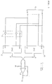
- Fig. 3 is a block diagram showing a composition of the aforementioned conventional digital-analog converter, wherein the digital-analog converter operates so as to output the difference of the output voltage between the two DACs, 10, 12, which operate with mutually opposite phases.
- An input digital signal 9 is inputted into the DAC 10 on one hand, and in inputted into the DAC 12 through an inverter 11 on the other hand.
- the output voltage of the DAC 10 and the output voltage of the DAC 12 have their phases inverted relatively, and by operating the difference of both DAC by an operational amplifier 13, it is possible to obtain two times the output voltage of each DAC.
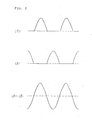
- Fig. 4 shows a relation of the output voltage waveform between each DAC in the aforementioned conventional digital-analog converter, in which the waveform A corresponds to the output voltage of the DAC 10 and the waveform B corresponds to the output voltage of the DAC 12.
- the waveform of A - B is the result of the subtraction of the waveform of A and the waveform of B, and the waveform of A - B becomes the output voltage obtained at the output terminal 14. That is, in the aforementioned example, when a sine wave is outputted, the output voltage waveform of each DAC also becomes the sine wave, so that the digital data to be inputted in either DAC will be inverted of all bits thereof when the waveform crosses zero.
- the present invention is designed in view of the above problems so as to prevent fundamentally the generation of "zero cross distortion" or glich in the output voltage waveform of each DAC, and intended to provide a digital-analog converter which can improve the fidelity considerably when reproducing analog signals of minute level in particular.
- the digital-analog converter of the present invention is equipped with a first DAC and a second DAC, an operational amplifier which carries out the addition and subtraction of the output voltage of the aforementioned first DAC and the output voltage of the aforementioned second DAC, when an analog signal of positive polarity is to be converted and outputted, the second DAC outputs a constant reference voltage, and when an analog signal of negative polarity is to be converted and outputted, the first DAC outputs a constant reference voltage.
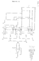
- Fig. 1 is a circuit diagram showing a composition of an embodiment of the present invention.
- the most significant bit of the input digital signal 1 is used as the positive/negative judgement signal to change an input digital signal to each DAC according to the positive state or the negative state of the polarity.
- the first data selector 2 is used to change the input digital signal of the first DAC 3, and operates so that when the input digital signal 1 is positive, the input digital signal from the second bit thereof to the least significant bit thereof are inputted into the first DAC 3, when the input digital signal is negative, "0" is inputted into all bits.
- the input digital signal 1 is converted into complement data by the complement operating device 4 to be inputted into the second data selector 5.
- the second data selector 5 is used to change the input digital signal of the second DAC 6, and operates so that when the input digital signal 1 is negative, complement of the input digital signal from the second bit thereof up to the least significant bit thereof is inputted into the second DAC 6, and when the input digital signal 1 is positive, "0" is inputted into all bits.
- the output voltage of each DAC is subtracted by the operational amplifier 7 and outputted at the output terminal 8.
- Fig. 2 shows the relation of the output voltage waveform between each DAC in the aforementioned embodiment, in which the waveform A corresponds to the output voltage of the first DAC 3 and the waveform B corresponds to the output voltage of the second DAC 6.
- the waveform of A - B is the result of the subtraction of the waveform of A and the waveform of B, and the waveform of A - B becomes the waveform obtained at the output terminal 8.
- each DAC is operating in a positive (or 0) range and will not be operating in a negative range. That is, each DAC will not cross zero and there will be no what is called "zero cross distortion" to be generated.
- the digital-analog converter of the present invention is equipped with a first DAC and a second DAC, an operational amplifier which carries out the addition and subtraction of the output voltage of the aforementioned first DAC and the output voltage of the aforementioned second DAC, when an analog signal of positive polarity is to be converted and outputted, and second DAC outputs a constant reference voltage, and when an analog signal of negative polarity is to be converted and outputted, the first DAC outputs a constant reference voltage. Therefore, the output voltage of each DAC is always positive (or 0) and there is no possibility of crossing zero.
- Fig. 1 is a circuit diagram showing the digital-analog converter of an embodiment of the present invention
- Fig. 2 is a waveform diagram showing the relation of the output voltage waveform between each DAC in the above embodiment
- Fig. 3 is a circuit diagram showing an example of the composition of a conventional digital-analog converter
- Fig. 4 is a waveform diagram showing the relation of the output voltage waveform between each DAC in the above conventional example.
Landscapes
- Engineering & Computer Science (AREA)
- Theoretical Computer Science (AREA)
- Analogue/Digital Conversion (AREA)
Abstract
The invention relates to a digital-analog converter (DAC), and is designed to prevent fundamentally "zero cross distortion" in the output voltage waveform of DAC or the generation of glitch and to improve the fidelity considerably when reproducing analog signals of minute level in particular, equipped with two DACs, a first DAC and a second DAC, and when reproducing a since wave for example, the digital-analog converter outputs the waveform corresponding to the input digital signal from the first DAC and outputs a certain reference voltage (0V for example) from the second DAC during a reproducing period of a positive half-wave.
Conversely, during a reproducing period of a negative half-wave, a positive waveform of which the input digital signal from the second DAC is inverted is outputted and a certain reference voltage (0V for example) is outputted from the first DAC. As a result of this, the output voltage of both DACs becomes positive or 0V so that the output voltage will not cross zero, and it becomes possible to eliminate "zero corss distortion" and the like.
Description
- The present invention relates to a digital-analog converter and is suitable for a digital audio equipment in that harmonic distortion or noise in particular can be reduced.
- The digital-analog converter (hereinafter called DAC) is an important constituent element which largely influences the performance of a digital audio equipment, but due to its composition, the DAC is susceptible to the influence of the supply voltage fluctuation, which used to cause the harmonic distortion or modulation distortion of audio signal.
- Further, because the DAC is consisted of a number of semiconductor devices, the DAC itself became a noise source causing S/N of the audio signal to deteriorate.
- As a means to improve the defect of the DAC as described above, a method which cancels the influence of the supply voltage fluctuation or the influence of noise by causing two DACs to operate with a push-pull has been suggested (Denpa Shimbun, March 13, 1987, Page 13).
- Fig. 3 is a block diagram showing a composition of the aforementioned conventional digital-analog converter, wherein the digital-analog converter operates so as to output the difference of the output voltage between the two DACs, 10, 12, which operate with mutually opposite phases.
- An input
digital signal 9 is inputted into theDAC 10 on one hand, and in inputted into theDAC 12 through an inverter 11 on the other hand. As a result of this entry, the output voltage of theDAC 10 and the output voltage of theDAC 12 have their phases inverted relatively, and by operating the difference of both DAC by anoperational amplifier 13, it is possible to obtain two times the output voltage of each DAC. - Fig. 4 shows a relation of the output voltage waveform between each DAC in the aforementioned conventional digital-analog converter, in which the waveform A corresponds to the output voltage of the
DAC 10 and the waveform B corresponds to the output voltage of theDAC 12. The waveform of A - B is the result of the subtraction of the waveform of A and the waveform of B, and the waveform of A - B becomes the output voltage obtained at theoutput terminal 14. That is, in the aforementioned example, when a sine wave is outputted, the output voltage waveform of each DAC also becomes the sine wave, so that the digital data to be inputted in either DAC will be inverted of all bits thereof when the waveform crosses zero. - As a result of inverting all bits while the waveform crosses zero, what is called "zero cross distortion" is generated or glich is generated thereby preventing high fidelity reproduction in many cases, but in the aforementioned example, there is no improvement as far as such high fidelity reproduction is concerned, allowing "zero cross distortion" or glich which is generated by each DAC is outputted as it is, and the effect of using two DACs is not so immediate.
- The present invention is designed in view of the above problems so as to prevent fundamentally the generation of "zero cross distortion" or glich in the output voltage waveform of each DAC, and intended to provide a digital-analog converter which can improve the fidelity considerably when reproducing analog signals of minute level in particular.
- In order to solve the above-mentioned problems, the digital-analog converter of the present invention is equipped with a first DAC and a second DAC, an operational amplifier which carries out the addition and subtraction of the output voltage of the aforementioned first DAC and the output voltage of the aforementioned second DAC, when an analog signal of positive polarity is to be converted and outputted, the second DAC outputs a constant reference voltage, and when an analog signal of negative polarity is to be converted and outputted, the first DAC outputs a constant reference voltage.
- The functions of the DAC of the present invention according to the aforementioned composition will be described as follows.
- That is, when reproducing a sine waveform for example, during a period wherein the positive half-wave is to be reproduced, a waveform corresponding to an input digital signal is outputted from the first DAC, and a constant reference voltage (0V for example) is outputted from the second DAC. Conversely, during a period wherein the negative half-wave is to be reproduced, the positive sine waveform which is inverted of an input digital signal is outputted from the second DAC, and a constant reference voltage (0V for example) is outputted from the first DAC. Consequently, the output voltage of either DAC becomes positive or 0V and will not cross zero, and it becomes possible to eliminate "zero cross distortion" and the like.
- Embodiments of the present invention will hereinafter be described with reference to the drawings.
- Fig. 1 is a circuit diagram showing a composition of an embodiment of the present invention.
- In the diagram, the most significant bit of the input
digital signal 1 is used as the positive/negative judgement signal to change an input digital signal to each DAC according to the positive state or the negative state of the polarity. Thefirst data selector 2 is used to change the input digital signal of thefirst DAC 3, and operates so that when the inputdigital signal 1 is positive, the input digital signal from the second bit thereof to the least significant bit thereof are inputted into thefirst DAC 3, when the input digital signal is negative, "0" is inputted into all bits. The inputdigital signal 1 is converted into complement data by thecomplement operating device 4 to be inputted into thesecond data selector 5. Thesecond data selector 5 is used to change the input digital signal of thesecond DAC 6, and operates so that when the inputdigital signal 1 is negative, complement of the input digital signal from the second bit thereof up to the least significant bit thereof is inputted into thesecond DAC 6, and when the inputdigital signal 1 is positive, "0" is inputted into all bits. The output voltage of each DAC is subtracted by theoperational amplifier 7 and outputted at theoutput terminal 8. - Fig. 2 shows the relation of the output voltage waveform between each DAC in the aforementioned embodiment, in which the waveform A corresponds to the output voltage of the
first DAC 3 and the waveform B corresponds to the output voltage of thesecond DAC 6. The waveform of A - B is the result of the subtraction of the waveform of A and the waveform of B, and the waveform of A - B becomes the waveform obtained at theoutput terminal 8. As can be known from Fig. 2, each DAC is operating in a positive (or 0) range and will not be operating in a negative range. That is, each DAC will not cross zero and there will be no what is called "zero cross distortion" to be generated. When the output waveform starts rising gradually from zero, input digital signal is changed in order from the lower bit, and as in the case of a conventional example, there is no possibility that all bits are inverted simultaneously. For this reason, it is difficult for glitch to be generated fundamentally, and a separate deglitch circuit is not necessary. As regards each DAC, because only the positive (or 0) output is required always, what is called the unipolar operation will suffice and it is not necessary to have bipolar operation as in the case of the conventional example. - As described above, the digital-analog converter of the present invention is equipped with a first DAC and a second DAC, an operational amplifier which carries out the addition and subtraction of the output voltage of the aforementioned first DAC and the output voltage of the aforementioned second DAC, when an analog signal of positive polarity is to be converted and outputted, and second DAC outputs a constant reference voltage, and when an analog signal of negative polarity is to be converted and outputted, the first DAC outputs a constant reference voltage. Therefore, the output voltage of each DAC is always positive (or 0) and there is no possibility of crossing zero. For this reason, what is called "zero cross distortion" will not be generated and the analog signal is changed in order from the lower bit in a minute signal level, and there is an effect the glich is difficult to be generated. Consequently, a high fidelity digital-analog converter is provided which is suitable for a digital audio equipment in which the distortion at a minute signal level in particular or noise becomes problematic.
- Fig. 1 is a circuit diagram showing the digital-analog converter of an embodiment of the present invention, Fig. 2 is a waveform diagram showing the relation of the output voltage waveform between each DAC in the above embodiment, Fig. 3 is a circuit diagram showing an example of the composition of a conventional digital-analog converter, and Fig. 4 is a waveform diagram showing the relation of the output voltage waveform between each DAC in the above conventional example.
Claims (3)
- (1) A digital-analog converter comprising a first digital-analog converter and a second digital-analog converter, an operational amplifier which carries out the addition and subtraction of the output voltage of the above first digital-analog converter and the above second digital-analog converter, when the analog signal of positive polarity is to be converted and outputted, the second digital-analog converter outputs a constant reference voltage, and when the analog signal of negative polarity is to be converted and outputted, the first digital-analog converter outputs a constant reference voltage.
- (2) A digital-analog converter according to claim 1, wherein when the analog signal of positive polarity is to be converted and outputted, "0" is inputted into all bits of the second digital-analog converter by the second data selector to cause a constant reference voltage to be outputted, and when the analog signal of negative polarity is to be converted and outputted, "0" is inputted into all bits of the first digital-analog converter by the first data selector to cause a constant reference voltage to be outputted.
- (3) A digital-analog converter according to claim 2, wherein when the analog signal of negative polarity is to be converted and outputted, complement data is inputted into the second digital-analog converter.
Applications Claiming Priority (2)
| Application Number | Priority Date | Filing Date | Title |
|---|---|---|---|
| JP62090269A JPS63256020A (en) | 1987-04-13 | 1987-04-13 | Digital/analog converter |
| JP90269/87 | 1987-04-13 |
Publications (2)
| Publication Number | Publication Date |
|---|---|
| EP0287312A2 true EP0287312A2 (en) | 1988-10-19 |
| EP0287312A3 EP0287312A3 (en) | 1992-05-13 |
Family
ID=13993787
Family Applications (1)
| Application Number | Title | Priority Date | Filing Date |
|---|---|---|---|
| EP19880303247 Withdrawn EP0287312A3 (en) | 1987-04-13 | 1988-04-12 | Digital-analog converter |
Country Status (4)
| Country | Link |
|---|---|
| EP (1) | EP0287312A3 (en) |
| JP (1) | JPS63256020A (en) |
| KR (1) | KR910009068B1 (en) |
| CN (1) | CN1011845B (en) |
Cited By (4)
| Publication number | Priority date | Publication date | Assignee | Title |
|---|---|---|---|---|
| AU614408B2 (en) * | 1988-11-14 | 1991-08-29 | Kollmorgen Corporation | Square root digital-to-analog converter |
| WO1997029547A1 (en) * | 1996-02-12 | 1997-08-14 | Advanced Micro Devices, Inc. | A digital to analog converter and dynamic current mirror structure to simplify on-chip wave shaping |
| US7456773B1 (en) * | 2007-06-14 | 2008-11-25 | Qualcomm Incorporated | Pseudo-differential class-AB digital-to-analog converter with code dependent DC current |
| RU2562371C1 (en) * | 2014-04-25 | 2015-09-10 | Леонид Анатольевич Бурцев | Method of adjustment of volume level |
Families Citing this family (10)
| Publication number | Priority date | Publication date | Assignee | Title |
|---|---|---|---|---|
| US4972188A (en) * | 1989-09-15 | 1990-11-20 | International Business Machines Corporation | Push pull double digital-to-analog converter |
| JPH03154519A (en) * | 1989-11-13 | 1991-07-02 | Advantest Corp | Bipolar d/a converter |
| JPH03238926A (en) * | 1990-02-15 | 1991-10-24 | Funai Denki Kenkyusho:Kk | Method for conversion and converter |
| JPH03117947U (en) * | 1990-03-17 | 1991-12-05 | ||
| JPH066229A (en) * | 1992-06-23 | 1994-01-14 | Mitsubishi Electric Corp | D/a converter |
| JP4588546B2 (en) * | 2005-06-13 | 2010-12-01 | 株式会社ケンウッド | Amplitude variable device and amplitude variable method |
| CN102055477B (en) * | 2010-11-29 | 2012-03-21 | 复旦大学 | Amplitude-interleaving analog digital composite signal processing circuit |
| CN103631296B (en) * | 2013-12-18 | 2016-03-30 | 海能达通信股份有限公司 | A kind of voltage regulator circuit system |
| JP2015201729A (en) * | 2014-04-07 | 2015-11-12 | ローム株式会社 | Mixer circuit, audio signal processing circuit, audio signal mixing method, on-vehicle audio device using the method, audio component device, and electronic apparatus |
| JP6748247B2 (en) * | 2019-03-04 | 2020-08-26 | ローム株式会社 | Audio signal processing circuit, vehicle-mounted audio device using the same, audio component device, electronic device |
Citations (4)
| Publication number | Priority date | Publication date | Assignee | Title |
|---|---|---|---|---|
| US3582939A (en) * | 1969-09-19 | 1971-06-01 | Honeywell Inc | Bipolar digital-to-analog converter |
| EP0079681A2 (en) * | 1981-11-12 | 1983-05-25 | Minnesota Mining And Manufacturing Company | Bipolar digital to analog converter |
| US4430642A (en) * | 1981-10-02 | 1984-02-07 | Westinghouse Electric Corp. | Digital-to-analog converter |
| US4488144A (en) * | 1980-05-01 | 1984-12-11 | Analogic Corporation | High linearity digital to analog converter |
Family Cites Families (1)
| Publication number | Priority date | Publication date | Assignee | Title |
|---|---|---|---|---|
| JPS57178417A (en) * | 1981-04-27 | 1982-11-02 | Hitachi Ltd | Digital to analog converting circuit |
-
1987
- 1987-04-13 JP JP62090269A patent/JPS63256020A/en active Pending
-
1988
- 1988-04-08 KR KR1019880003974A patent/KR910009068B1/en not_active IP Right Cessation
- 1988-04-12 EP EP19880303247 patent/EP0287312A3/en not_active Withdrawn
- 1988-04-12 CN CN88102773A patent/CN1011845B/en not_active Expired
Patent Citations (4)
| Publication number | Priority date | Publication date | Assignee | Title |
|---|---|---|---|---|
| US3582939A (en) * | 1969-09-19 | 1971-06-01 | Honeywell Inc | Bipolar digital-to-analog converter |
| US4488144A (en) * | 1980-05-01 | 1984-12-11 | Analogic Corporation | High linearity digital to analog converter |
| US4430642A (en) * | 1981-10-02 | 1984-02-07 | Westinghouse Electric Corp. | Digital-to-analog converter |
| EP0079681A2 (en) * | 1981-11-12 | 1983-05-25 | Minnesota Mining And Manufacturing Company | Bipolar digital to analog converter |
Cited By (5)
| Publication number | Priority date | Publication date | Assignee | Title |
|---|---|---|---|---|
| AU614408B2 (en) * | 1988-11-14 | 1991-08-29 | Kollmorgen Corporation | Square root digital-to-analog converter |
| WO1997029547A1 (en) * | 1996-02-12 | 1997-08-14 | Advanced Micro Devices, Inc. | A digital to analog converter and dynamic current mirror structure to simplify on-chip wave shaping |
| US5861830A (en) * | 1996-02-12 | 1999-01-19 | Advanced Micro Devices, Inc. | Digital to analog converter and dynamic current mirror structure to simplify on-chip wave shaping |
| US7456773B1 (en) * | 2007-06-14 | 2008-11-25 | Qualcomm Incorporated | Pseudo-differential class-AB digital-to-analog converter with code dependent DC current |
| RU2562371C1 (en) * | 2014-04-25 | 2015-09-10 | Леонид Анатольевич Бурцев | Method of adjustment of volume level |
Also Published As
| Publication number | Publication date |
|---|---|
| CN1011845B (en) | 1991-02-27 |
| KR880013328A (en) | 1988-11-30 |
| KR910009068B1 (en) | 1991-10-28 |
| JPS63256020A (en) | 1988-10-24 |
| EP0287312A3 (en) | 1992-05-13 |
| CN88102773A (en) | 1988-11-02 |
Similar Documents
| Publication | Publication Date | Title |
|---|---|---|
| EP0287312A2 (en) | Digital-analog converter | |
| JP2573850B2 (en) | Analog-to-digital converter | |
| US6362765B2 (en) | D/A converter | |
| EP0264921A2 (en) | A digital to analog converter | |
| EP0383689A2 (en) | Digital-to-analog converter | |
| JPS61191125A (en) | Digital-analog converter | |
| US4665381A (en) | Digital-to-analog converter | |
| US4498072A (en) | A/D Converter having a self-bias circuit | |
| US5021785A (en) | Floating point digital to analog converter with bias to establish range midpoint | |
| JPH0621814A (en) | Digital-to-analog converter provided with precise linear output for both positive and negative input values | |
| JP2579555B2 (en) | Digital / analog converter | |
| JP2599207B2 (en) | Digital-to-analog converter | |
| JP3018681B2 (en) | D / A converter | |
| US6229470B1 (en) | Analog clipping circuit for mixed signal codecs | |
| EP0279993A2 (en) | A circuit for removing unwanted temporal portions of a voltage varying signal | |
| KR100302591B1 (en) | Digital to analog converter | |
| JP2751177B2 (en) | Digital-to-analog converter | |
| US4855741A (en) | Logarithmic digital level display device | |
| SU1765893A1 (en) | Multiplying digital-to-analog converter | |
| JPH0964745A (en) | Optional waveform generator | |
| JP2662955B2 (en) | Digital-to-analog conversion circuit | |
| JPS60256228A (en) | Digital-analog converter | |
| KR19990010734A (en) | FM signal asymmetry correction device in optical disk system | |
| JPH05114298A (en) | Digital data storing/reproducing apparatus | |
| EP0177902B1 (en) | Digital-to-analog converter |
Legal Events
| Date | Code | Title | Description |
|---|---|---|---|
| PUAI | Public reference made under article 153(3) epc to a published international application that has entered the european phase |
Free format text: ORIGINAL CODE: 0009012 |
|
| AK | Designated contracting states |
Kind code of ref document: A2 Designated state(s): DE GB |
|
| PUAL | Search report despatched |
Free format text: ORIGINAL CODE: 0009013 |
|
| AK | Designated contracting states |
Kind code of ref document: A3 Designated state(s): DE GB |
|
| STAA | Information on the status of an ep patent application or granted ep patent |
Free format text: STATUS: THE APPLICATION IS DEEMED TO BE WITHDRAWN |
|
| 18D | Application deemed to be withdrawn |
Effective date: 19921114 |