EP0285523A1 - Optical-fibre delay line for coherent signal processing, and its uses in filtering, correlation, and spectral analysis - Google Patents
Optical-fibre delay line for coherent signal processing, and its uses in filtering, correlation, and spectral analysis Download PDFInfo
- Publication number
- EP0285523A1 EP0285523A1 EP88400803A EP88400803A EP0285523A1 EP 0285523 A1 EP0285523 A1 EP 0285523A1 EP 88400803 A EP88400803 A EP 88400803A EP 88400803 A EP88400803 A EP 88400803A EP 0285523 A1 EP0285523 A1 EP 0285523A1
- Authority
- EP
- European Patent Office
- Prior art keywords
- modulators
- fiber
- optical
- coupler
- optical fiber
- Prior art date
- Legal status (The legal status is an assumption and is not a legal conclusion. Google has not performed a legal analysis and makes no representation as to the accuracy of the status listed.)
- Withdrawn
Links
Images

Classifications
-
- G—PHYSICS
- G02—OPTICS
- G02F—OPTICAL DEVICES OR ARRANGEMENTS FOR THE CONTROL OF LIGHT BY MODIFICATION OF THE OPTICAL PROPERTIES OF THE MEDIA OF THE ELEMENTS INVOLVED THEREIN; NON-LINEAR OPTICS; FREQUENCY-CHANGING OF LIGHT; OPTICAL LOGIC ELEMENTS; OPTICAL ANALOGUE/DIGITAL CONVERTERS
- G02F1/00—Devices or arrangements for the control of the intensity, colour, phase, polarisation or direction of light arriving from an independent light source, e.g. switching, gating or modulating; Non-linear optics
- G02F1/01—Devices or arrangements for the control of the intensity, colour, phase, polarisation or direction of light arriving from an independent light source, e.g. switching, gating or modulating; Non-linear optics for the control of the intensity, phase, polarisation or colour
- G02F1/21—Devices or arrangements for the control of the intensity, colour, phase, polarisation or direction of light arriving from an independent light source, e.g. switching, gating or modulating; Non-linear optics for the control of the intensity, phase, polarisation or colour by interference
- G02F1/225—Devices or arrangements for the control of the intensity, colour, phase, polarisation or direction of light arriving from an independent light source, e.g. switching, gating or modulating; Non-linear optics for the control of the intensity, phase, polarisation or colour by interference in an optical waveguide structure
- G02F1/2252—Devices or arrangements for the control of the intensity, colour, phase, polarisation or direction of light arriving from an independent light source, e.g. switching, gating or modulating; Non-linear optics for the control of the intensity, phase, polarisation or colour by interference in an optical waveguide structure in optical fibres
-
- G—PHYSICS
- G06—COMPUTING; CALCULATING OR COUNTING
- G06E—OPTICAL COMPUTING DEVICES; COMPUTING DEVICES USING OTHER RADIATIONS WITH SIMILAR PROPERTIES
- G06E3/00—Devices not provided for in group G06E1/00, e.g. for processing analogue or hybrid data
- G06E3/001—Analogue devices in which mathematical operations are carried out with the aid of optical or electro-optical elements
- G06E3/003—Analogue devices in which mathematical operations are carried out with the aid of optical or electro-optical elements forming integrals of products, e.g. Fourier integrals, Laplace integrals, correlation integrals; for analysis or synthesis of functions using orthogonal functions
-
- G—PHYSICS
- G06—COMPUTING; CALCULATING OR COUNTING
- G06E—OPTICAL COMPUTING DEVICES; COMPUTING DEVICES USING OTHER RADIATIONS WITH SIMILAR PROPERTIES
- G06E3/00—Devices not provided for in group G06E1/00, e.g. for processing analogue or hybrid data
- G06E3/001—Analogue devices in which mathematical operations are carried out with the aid of optical or electro-optical elements
- G06E3/005—Analogue devices in which mathematical operations are carried out with the aid of optical or electro-optical elements using electro-optical or opto-electronic means
Definitions
- the invention relates to the field of signal processing, and in particular to processing using optical waves.
- optical waves to transmit information via optical waveguides, in particular by optical fibers, has multiple advantages, in particular because of the very low sensitivity of this type of guides to disturbances. Beyond the simple aspects of transmission, a certain number of applications of this optical signal transmission have made it possible to highlight interesting properties which will lead to the use of these optical guides also for the processing of the information transmitted on these guides. .
- the use of single-mode optical fibers as delay lines is advantageous in particular for the processing of wideband microwave signals.
- the dispersion performance of optical fibers more than 100 GHZ per kilometer, and attenuation, less than 0.5 dB per kilometer, make it possible to envisage bandwidth-delay products greater than 5 ⁇ 105 with delays of the order of several tens of microseconds.
- single-mode fibers for guidance can be fully exploited because it has been possible to develop suitable light sources and III-V semiconductor detectors, as well as integrated optical circuits performing the useful functions, for example coupling or modulation.
- the applicant company has moreover already described in the information bulletin of its research laboratory, in December 1986, the creation of a delay line with 5 GHz of band and 5 microseconds of delay.
- the optical carrier could be used for coherent processing, but in this case the relative phases of the optical carrier at each of the signal taps should be stable up to a fraction of the optical wavelength. This would require a very stable, narrow source spectrum; moreover the differences in optical path should also be constant up to a fraction of the wavelength. For this reason, coherent detection, which depends on the phase of the optical carrier, is not implemented in devices using delay lines with single-mode fibers.
- the subject of the invention is a signal processing device with optical delay line, which allows coherent processing of the transmitted signal and which therefore avoids the drawbacks of systems where only quadratic detection is possible, and opens up great possibilities of applications. .
- a signal processing device using a single-mode optical fiber is characterized in that, to carry out coherent processing, the device comprises a ring interferometer, the ring of which is the single-mode optical fiber, the two ends of the fiber being coupled to two ports of a bidirectional coupler, to another port of which a source intended is coupled providing a continuous optical wave, the two counter-rotating optical waves in the ring being combined at the output in the coupler to form interference analyzed by a detector coupled to the fourth port of the coupler, an electrooptic phase modulator placed at one end of the fiber introducing a pre-established phase shift at the rate of the travel time in the fiber to fix the operating point on the sinusoidal response of the interferometer according to the phase shift, the processing device further comprising phase modulators controlled by the signals to be processed placed on the fiber.
- a series of phase modulators are distributed equally over the fiber and controlled by the same signal to perform filtering functions, the interferometer being placed at an operating point where its characteristic is linear .
- phase modulators are arranged near the two ends of the fiber and controlled by different signals of which the product is to be produced, the interferometer being placed at an operating point where its characteristic is quadratic, to perform correlation functions or perform spectral analysis.
- the signal processing device using a tapped delay line, optical fiber comprises a source 1 which emits an optical wave pulse to which is coupled a single mode optical fiber 10 on which are distributed a certain number of taps P0, P1, P2 ... P n equidistant, the delay introduced between two consecutive taps, P i and P i + 1 , being equal to ⁇ ; the signals from these different sockets are transmitted via attenuators A0, A1, A2 .... A n at the inputs of a quadratic detector 30.
- the output signal of this quadratic detector is therefore the sum, weighted by the attenuators A0 ... A n , signals from the different taps P0 ... P n successively delayed by ⁇ .
- the defect of such a processing device is that it can only process positive signals, possibly by weighting them, due to the type of detection that can be used. Consequently, the weighting by negative coefficients is excluded for this type of system, except by using devices by which the outputs of the different sockets are combined in one or the other of two detectors depending on whether they are to be assigned a positive or negative coefficient, the outputs of these two detectors then being combined with different signs.
- FIG. 2 represents a delay line with optical fiber, called recirculation, according to the prior art.
- This structure comprises a source 1 which emits an optical wave pulse, an optical fiber loop 15 and a directional coupler 20 arranged in the following manner: the source 1 is connected to the first port A of the coupler, the optical fiber loop is connected between an opposite access C of the coupler and the conjugate access of A, B, and the output of the device takes place on the second opposite access D.
- the first pass a fraction of the optical wave is transmitted to the output D while the other fraction travels through the loop 15.
- On the second pass a fraction of the optical wave is transmitted to the output D and the other part recirculates in the loop 15 etc ...
- FIG. 3 represents a first embodiment of the signal processing device according to the invention.
- This device comprises a source 1 intended to emit a continuous optical wave, connected to a first access A of a bidirectional coupler (with fiber or integrated optics for example) 20.
- a bidirectional coupler with fiber or integrated optics for example
- To the two opposite accesses C and D of the directional coupler 20 are connected the two ends of a loop of single-mode optical fiber 25 at one end of which are mounted in series along the optical fiber of the electrooptical modulators M1, M2, etc ... M n ; two successive modulators M i , M i + 1 are connected by pieces of optical fiber of identical lengths introducing a delay equal to ⁇ i, i + 1 .
- These modulators are controlled by an electrical impulse control signal applied to the input E C.
- a phase modulator M G controlled by a signal of period equal to the propagation time in the fiber, is placed on the fiber at the other end to introduce a fixed phase shift between the two waves counter-rotating circulating in the fiber, fixing the operating point.
- a detector 30 is connected to the fourth access B of the coupler 20.
- the phase shifts can be added or subtracted on the quadratic detector within the limit of the linearity zone of the sinusoidal response of the interferometer set by the modulator M G.
- the processing possibilities are much greater.
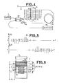
- FIG. 4 represents a particular embodiment of the coherent signal processing device according to the invention. Like the previous one, it includes a source 1, a bidirectional coupler 20, a coil of single-mode optical fiber 25 at one end of which are placed in series on the optical fiber of the basic modulators, and at the other end of which is placed the modulator M G . However, in this embodiment, the modulators are all produced on the same circuit M.
- G n , n 11 in the figure, provided with control electrodes arranged in a conventional manner on either side of the guide, and not shown in the figure, for the introduction of a phase shift due to the electric field applied to the guides.
- Pieces of optical fiber of length adapted to the delay ⁇ to be introduced between two modulators connect the output of one guide to the input of the next, for example according to the configuration shown in FIG. 4, where the output of a modulator and the input of the next modulator are produced on the same side face of the integrated optical circuit.
- This arrangement is not limiting and all the inputs of the modulators can be arranged on the same lateral face of the integrated optical circuit and all the outputs on the other face, optical fiber loops being adapted accordingly.
- the access to the directional coupler located on the same side as the source is connected to a detector 30.
- the electrical signal applied to the control input E C is an electrical pulse which introduces a phase modulation of the optical wave simultaneously on the light wave propagating on the optical figure, and therefore at times spaced from ⁇ on l continuous optical wave transmitted by the source.
- the length of the electrodes of each of the elementary modulators, whether they are produced independently or produced on the same integrated optical circuit determines the phase shift applied, and the direction of this phase shift is fixed by the direction of the electric field applied to these electrodes. By a particular configuration of the electrodes it is therefore possible to obtain phase shifts ⁇ 1 (t) and ⁇ 2 (t) on the two counter-rotating ⁇ 1 and ⁇ 2 waves in the fiber loop 25. An example of these phase shifts is shown in FIG.
- the wave ⁇ 1 first undergoes modulation by the modulator produced from the guide G1 while the counter-rotating wave ⁇ 2 first undergoes a phase shift by the modulator produced from the guide G11.
- FIG. 6 partially represents an embodiment of the modulator M where the control electrodes of the phase modulators have been represented, assuming that the phase shifts applied are those represented in FIG. 5.
- Each guide G1, G2, G3, G4 is associated with suitably configured control electrodes. These control electrodes are interconnected. In the example shown, the control voltage has the same direction for the first four modulators.
- the invention is not limited to the embodiments described and shown.
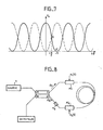
- the linear part of the sinusoidal response of the interferometer shown in FIG. 7 is used to detect phase differences.
- the interferometer is placed "at an angle" in the linear zone, that is to say that a phase modulator, M G , placed at one end of the fiber creates an additional phase modulation alternately of + and - , at the rate of the fiber travel time and therefore a additional phase shift equal to which places the operating point of the interferometer at point G of the sinusoidal response, FIG. 7, the phase variations resulting in power variations around this point.
- the non-linear part of the sinusoidal response of the interferometer can detect signals whose processing has been carried out at high frequency, for example around 10 GHz, in a lower frequency band, 10 to 100 MHz for example.
- This processing using the quadratic part of the response of the interferometer as a function of the phase applies for example to the performance of functions such as inter-correlation, auto-correlation or spectrum analysis.
- FIG. 8 illustrates an embodiment of the processing device according to the invention: a source 1 is connected to the first access A of a 3dB coupler, 20, which distributes the incident optical wave between the two ends of a loop of optical fiber 25, themselves coupled to the ports C and D of the coupler 20.
- Two phase modulators M ⁇ 1 and M ⁇ 2 controlled by electrical signals respectively s1 (t) and s2 (t) create phase modulations respectively ⁇ 1 (t) and ⁇ 2 (t).
- the phase difference between the two counter-rotating waves is ⁇ , that is to say that the operating point on the characteristic of FIG. 7 is G ⁇
- the intensity of the light on the detector 30 coupled to the fourth port, B, of the coupler 20 is a function of the product ⁇ 1 (t) . ⁇ 2 (t).
- the detected intensity is a function of ⁇ 1 (t) ⁇ 2 (t) dt where td is the detector response time.
- the optical fiber 25 between M ⁇ 1 and M ⁇ 2 can be a fiber with high dispersion so that the information applied via s1 (t) on the wave traversing the fiber in the direction "-" is filtered, and likewise for the information applied via s2 (t) on the wave traversing the fiber in the direction "+".
- the optical wave can be amplified by any known means.
- This amplification, in the loop, or even downstream, can for example be carried out by stimulated "RAMAN” effect (by transfer of energy from a pump signal to the optical wave), by optical semiconductor amplification, or by coupling of waves.
- s1 (t) s (t)
- signal to be analyzed s2 (t) cos ⁇ t (or sin ⁇ t)
- ⁇ 2 ⁇ (f + f ⁇ t)
- This signal is therefore directly linked to the Fourier transform of s (t): s (t) cos ( ⁇ t) dt It is possible to obtain the real part or the imaginary part of the Fourier transform using two similar circuits.
- the structure represented in FIG. 3 with several modulators controlled by the same signal, ie s (t), can be associated with the structure represented in FIG. 8 for allow the signal to be repeated, at a rate equal to the propagation time between modulators, a number of times equal to the number of modulators:
- the modulator M G shown in FIGS. 3, 4 and 8 can in practice be integrated with the bidirectional coupler 20, the device thus using a multifunction integrated optical circuit.
Landscapes
- Physics & Mathematics (AREA)
- Nonlinear Science (AREA)
- Engineering & Computer Science (AREA)
- Theoretical Computer Science (AREA)
- Mathematical Physics (AREA)
- Optics & Photonics (AREA)
- General Physics & Mathematics (AREA)
- Optical Communication System (AREA)
- Optical Integrated Circuits (AREA)
Abstract
Description
L'invention se rapporte au domaine du traitement de signal, et notamment à un traitement utilisant des ondes optiques.The invention relates to the field of signal processing, and in particular to processing using optical waves.
L'utilisation d'ondes optiques pour transmettre des informations par l'intermédiaire de guides d'ondes optiques, notamment par des fibres optiques, présente de multiples intérêts notamment du fait de la très faible sensibilité de ce type de guides aux perturbations. Au delà des simples aspects de transmission, un certain nombre d'applications de cette transmission optique de signal ont permis de mettre en évidence des propriétés intéressantes qui vont amener à l'utilisation de ces guides optiques également pour le traitement des informations transmises sur ces guides.The use of optical waves to transmit information via optical waveguides, in particular by optical fibers, has multiple advantages, in particular because of the very low sensitivity of this type of guides to disturbances. Beyond the simple aspects of transmission, a certain number of applications of this optical signal transmission have made it possible to highlight interesting properties which will lead to the use of these optical guides also for the processing of the information transmitted on these guides. .
En particulier, l'utilisation des fibres optiques monomodes comme lignes à retard est intéressante notamment pour le traitement des signaux hyperfréquences large bande. En effet les performances de dispersion des fibres optiques, plus de 100 GHZ par kilomètre, et d'atténuation, moins de 0,5 dB par kilomètre, permettent d'envisager des produits bande passante-retard supérieurs à 5×10⁵ avec des retards de l'ordre de plusieurs dizaines de microsecondes.In particular, the use of single-mode optical fibers as delay lines is advantageous in particular for the processing of wideband microwave signals. Indeed, the dispersion performance of optical fibers, more than 100 GHZ per kilometer, and attenuation, less than 0.5 dB per kilometer, make it possible to envisage bandwidth-delay products greater than 5 × 10⁵ with delays of the order of several tens of microseconds.
Les performances des fibres monomodes pour le guidage sont complètement exploitables du fait qu'on a pu mettre au point des sources de lumière et des détecteurs à semi-conducteurs III-V adaptés, ainsi que des circuits optiques intégrés réalisant les fonctions utiles, par exemple couplage ou modulation.The performance of single-mode fibers for guidance can be fully exploited because it has been possible to develop suitable light sources and III-V semiconductor detectors, as well as integrated optical circuits performing the useful functions, for example coupling or modulation.
La société demanderesse a d'ailleurs déjà décrit dans le bulletin d'informations de son laboratoire de recherches, en décembre 1986, la réalisation d'une ligne à retard de 5 GHz de bande et 5 microsecondes de retard.The applicant company has moreover already described in the information bulletin of its research laboratory, in December 1986, the creation of a delay line with 5 GHz of band and 5 microseconds of delay.
Du fait de ces grandes possibilités, l'utilisation de fibres optiques monomodes pour le traitement a déjà été envisagée notamment comme lignes à retard dans un article intitulé "Optical fiber delay line signal processing" de IEEE Transaction on Microwave Theroy and Techniques, vol. MTT 33, n°3, mars 1985. Cet article décrit notamment des lignes à prises et des lignes à re-circulation dans lesquelles la fibre optique ou des boucles de celle-ci sont utilisées pour introduire des retards sur le signal transmis. Les lignes à retard ainsi constituées combinent de manière incohérente les signaux issus des différentes prises aménagées à cet effet le long de la ligne à retard.Because of these great possibilities, the use of single-mode optical fibers for processing has already been envisaged in particular as delay lines in an article entitled "Optical fiber delay line signal processing" by IEEE Transaction on Microwave Theroy and Techniques, vol. MTT 33, n ° 3, March 1985. This article describes in particular tap lines and recirculation lines in which optical fiber or loops thereof are used to introduce delays on the transmitted signal. The delay lines thus formed incoherently combine the signals from the different sockets fitted for this purpose along the delay line.
En théorie la porteuse optique pourrait être utilisée pour du traitement cohérent, mais dans ce cas il faudrait que les phases relatives de la porteuse optique à chacune des prises de signal soient stables jusqu'à une fraction de la longueur d'onde optique. Cela requérerait un spectre de source étroit, très stable ; de plus les différences de chemin optique devraient également être constantes jusqu'à une fraction de la longueur d'onde. Pour cette raison la détection cohérente, qui dépend de la phase de la porteuse optique, n'est pas mise en oeuvre dans les dispositifs utilisant des lignes à retard à fibres monomodes.In theory, the optical carrier could be used for coherent processing, but in this case the relative phases of the optical carrier at each of the signal taps should be stable up to a fraction of the optical wavelength. This would require a very stable, narrow source spectrum; moreover the differences in optical path should also be constant up to a fraction of the wavelength. For this reason, coherent detection, which depends on the phase of the optical carrier, is not implemented in devices using delay lines with single-mode fibers.
Seule la sommation incohérente par des détecteurs quadratiques, est possible, et la pondération éventuellement négative des signaux issus des différentes prises sur une ligne à retard à fibre optique monomode, pour réaliser des fonctions de filtrage, ne peut pas être accomplie optiquement.Only incoherent summation by quadratic detectors is possible, and the possibly negative weighting of the signals coming from the different taps on a delay line with single mode optical fiber, to perform filtering functions, cannot be accomplished optically.
L'invention a pour objet un dispositif de traitement de signal avec ligne à retard optique, qui autorise un traitement cohérent du signal transmis et qui donc évite les inconvénients des systèmes où seule la détection quadratique est possible, et ouvre de grandes possibilités d'applications.The subject of the invention is a signal processing device with optical delay line, which allows coherent processing of the transmitted signal and which therefore avoids the drawbacks of systems where only quadratic detection is possible, and opens up great possibilities of applications. .
Selon l'invention, un dispositif de traitement de signal utilisant une fibre optique monomode, est caractérisé en ce que, pour effectuer un traitement cohérent, le dispositif comporte un interféromètre en anneau dont l'anneau est la fibre optique monomode, les deux extrémités de la fibre étant couplées à deux accès d'un coupleur bidirectionnel, à un autre accès duquel est couplée une source destinée à fournir une onde optique continue, les deux ondes optiques contrarotatives dans l'anneau étant combinées en sortie dans le coupleur pour former des interférences analysées par un détecteur couplé au quatrième accès du coupleur, un modulateur de phase électrooptique placé à une extrémité de la fibre introduisant un déphasage préétabli au rythme du temps de parcours dans la fibre pour fixer le point de fonctionnement sur la réponse sinusoïdale de l'interféromètre en fonction du déphasage, le dispositif de traitement comportant en outre des modulateurs de phase commandés par les signaux à traiter placés sur la fibre.According to the invention, a signal processing device using a single-mode optical fiber, is characterized in that, to carry out coherent processing, the device comprises a ring interferometer, the ring of which is the single-mode optical fiber, the two ends of the fiber being coupled to two ports of a bidirectional coupler, to another port of which a source intended is coupled providing a continuous optical wave, the two counter-rotating optical waves in the ring being combined at the output in the coupler to form interference analyzed by a detector coupled to the fourth port of the coupler, an electrooptic phase modulator placed at one end of the fiber introducing a pre-established phase shift at the rate of the travel time in the fiber to fix the operating point on the sinusoidal response of the interferometer according to the phase shift, the processing device further comprising phase modulators controlled by the signals to be processed placed on the fiber.
Dans un premier mode de réalisation particulièrement adapté au filtrage, une série de modulateurs de phase sont équirépartis sur la fibre et commandés par le même signal pour réaliser des fonctions de filtrage, l'interféromètre étant placé à un point de fonctionnement où sa caractéristique est linéaire.In a first embodiment particularly suitable for filtering, a series of phase modulators are distributed equally over the fiber and controlled by the same signal to perform filtering functions, the interferometer being placed at an operating point where its characteristic is linear .
Dans un autre mode de réalisation deux modulateurs de phase sont disposés à proximité des deux extrémités de la fibre et commandés par des signaux différents dont on souhaite faire le produit, l'interféromètre étant placé à un point de fonctionnement où sa caractéristique est quadratique, pour réaliser des fonctions de corrélation ou effectuer une analyse spectrale.In another embodiment, two phase modulators are arranged near the two ends of the fiber and controlled by different signals of which the product is to be produced, the interferometer being placed at an operating point where its characteristic is quadratic, to perform correlation functions or perform spectral analysis.
L'invention sera mieux comprise et d'autres caractéristiques apparaîtront à l'aide de la description qui suit en référence aux figures annexées.
- - La figure 1 représente une ligne à retard à prise utilisant une fibre optique, selon l'art antérieur ;
- - La figure 2 est une ligne à re-circulation, utilisant une fibre optique, selon l'art antérieur ;
- - La figure 3 est un dispositif de traitement selon l'invention dans un premier mode de réalisation ;
- - La figure 4 est un second mode de réalisation du dispositif de traitement utilisant une ligne à retard à fibre optique selon l'invention ;
- - La figure 5 est un diagramme de signaux explicatifs ;
- - La figure 6 représente un mode de réalisation d'un modulateur M ;
- - La figure 7 représente la réponse sinusoïdale de l'interféromètre ;
- - La figure 8 représente un troisième mode de réalisation du dispositif de traitement selon l'invention.
- - Figure 1 shows a delay line taken using an optical fiber, according to the prior art;
- - Figure 2 is a re-circulation line, using an optical fiber, according to the prior art;
- - Figure 3 is a processing device according to the invention in a first embodiment;
- - Figure 4 is a second embodiment of the processing device using a fiber optic delay line according to the invention;
- - Figure 5 is a diagram of explanatory signals;
- - Figure 6 shows an embodiment of a modulator M;
- - Figure 7 shows the sinusoidal response of the interferometer;
- - Figure 8 shows a third embodiment of the processing device according to the invention.
Le dispositif de traitement de signal utilisant une ligne à retard à prises, à fibre optique, selon l'art antérieur comporte une source 1 qui émet une impulsion d'onde optique à laquelle est couplée une fibre optique monomode 10 sur laquelle sont réparties un certain nombre de prises P₀, P₁, P₂ ... Pn équidistantes, le retard introduit entre deux prises consécutives, Pi et Pi+1, étant égal à τ ; les signaux issus de ces différentes prises sont transmis via des atténuateurs respectivement A₀, A₁, A₂ .... An aux entrées d'un détecteur quadratique 30. Le signal de sortie de ce détecteur quadratique est donc la somme, pondérée par les atténuateurs A₀ ... An, des signaux issus des différentes prises P₀ ... Pn successivement retardés de τ.The signal processing device using a tapped delay line, optical fiber, according to the prior art comprises a
Comme indiqué ci-dessus, le défaut d'un tel dispositif de traitement est qu'il ne peut traiter que des signaux positifs, éventuellement en les pondérant, du fait du type de détection utilisable. En conséquence la pondération par des coefficients négatifs est exclue pour ce type de système, sauf en utilisant des artifices par lesquels les sorties des différentes prises sont combinées dans l'un ou l'autre de deux détecteurs selon qu'ils doivent être affectés d'un coefficient positif ou négatif, les sorties de ces deux détecteurs étant alors combinées avec des signes différents.As indicated above, the defect of such a processing device is that it can only process positive signals, possibly by weighting them, due to the type of detection that can be used. Consequently, the weighting by negative coefficients is excluded for this type of system, except by using devices by which the outputs of the different sockets are combined in one or the other of two detectors depending on whether they are to be assigned a positive or negative coefficient, the outputs of these two detectors then being combined with different signs.
La figure 2 représente une ligne à retard à fibre optique, dite à re-circulation, selon l'art antérieur. Cette structure comporte une source 1 qui émet une impulsion d'onde optique, une boucle de fibre optique 15 et un coupleur directionnel 20 arrangé de la manière suivante : la source 1 est reliée au premier accès A du coupleur, la boucle de fibre optique est branchée entre un accès opposé C du coupleur et l'accès conjugué de A,B, et la sortie du dispositif s'effectue sur le second accès opposé D. Ainsi au premier passage une fraction de l'onde optique est transmise à la sortie D tandis que l'autre fraction parcourt la boucle 15. Au second passage une fraction de l'onde optique est transmise à la sortie D et l'autre partie re-circule dans la boucle 15 etc... On obtient ainsi, entre les impulsions de sortie, des retards strictement égaux puisque le trajet optique est le même.FIG. 2 represents a delay line with optical fiber, called recirculation, according to the prior art. This structure comprises a
Comme le dispositif représenté sur la figure 1, celui représenté sur la figure 2 ne permet pas d'effectuer sur le signal un traitement cohérent.Like the device represented in FIG. 1, that represented in FIG. 2 does not allow coherent processing to be carried out on the signal.
La figure 3 représente un premier mode de réalisation du dispositif de traitement de signal selon l'invention. Ce dispositif comporte une source 1 destinée à émettre une onde optique continue, reliée à un premier accès A d'un coupleur bidirectionnel (à fibre ou optique intégrée par exemple) 20. Aux deux accès opposés C et D du coupleur directionnel 20 sont reliées les deux extrémités d'une boucle de fibre optique monomode 25 à une extrémité de laquelle sont montés en série le long de la fibre optique des modulateurs électrooptiques M₁, M₂, etc... Mn ; deux modulateurs Mi, Mi+1 successifs sont reliés par des morceaux de fibre optique de longueurs identiques introduisant un retard égal à τi,i+1. Ces modulateurs sont commandés par un signal électrique de commande impulsionnel appliqué à l'entrée EC. Un modulateur de phase MG, commandé par un signal de période égale au temps de propagation dans la fibre, est placé sur la fibre à l'autre extrémité pour introduire un déphasage fixe entre les deux ondes contra-rotatives circulant dans la fibre, fixant le point de fonctionnement. Un détecteur 30 est branché au quatrième accès B du coupleur 20. Cette structure est celle d'un interféromètre en anneau, dans l'anneau duquel sont placés ensérie plusieurs modulateurs de phase en optique intégrée, séparés par des retards τi,i+1. Typiquement τ = 5 nanosecondes pour un mètre de fibre optique. Ces modulateurs, commandés par le même signal de commande impulsionnel, vont introduire des déphasages impulsionnels espacés de τ sur le signal continu transmis dans la boucle. Lorsque les signaux repassent sur le coupleur bidirectionnel où les ondes interfèrent, les déphasages pourront s'ajouter ou se soustraire sur le détecteur quadratique dans la limite de la zone de linéarité de la réponse sinusoïdale de l'interféromètre fixée par le modulateur MG. Par rapport au système antérieur comportant une ligne à prises du type de celle décrite sur la figure 1, les possibilités de traitement sont beaucoup plus importantes.FIG. 3 represents a first embodiment of the signal processing device according to the invention. This device comprises a
La figure 4 représente un mode particulier de réalisation du dispositif de traitement de signal cohérent selon l'invention. Il comporte comme le précédent une source 1, un coupleur bidirectionnel 20, une bobine de fibre optique monomode 25 à une extrémité duquel sont placés en série sur la fibre optique des modulateurs élémentaires, et à l'autre extrémité duquel est placé le modulateur MG. Mais dans ce mode de réalisation les modulateurs sont tous réalisés sur le même circuit M. Ce circuit est un circuit optique intégré de largeur l = 10 à 20 mm, selon la modulation de phase souhaitée, et à la surface duquel sont prévus des guides optiques, G₁, G₂ ... Gn, n = 11 sur la figure, munis d'électrodes de commande disposées de manière classique de part et d'autre du guide, et non représentées sur la figure, pour l'introduction d'un déphasage du fait du champ électrique appliqué aux guides. Des morceaux de fibre optique de longueur adaptée au retard τ à introduire entre deux modulateurs relient la sortie d'un guide à l'entrée du suivant, par exemple selon la configuration représentée sur la figure 4, où la sortie d'un modulateur et l'entrée du modulateur suivant sont réalisées sur une même face latérale du circuit optique intégré. Cette disposition n'est pas limitative et toutes les entrées des modulateurs pourront être disposées sur la même face latérale du circuit optique intégrée et toutes les sorties sur l'autre face, des boucles de fibre optique étant adaptées en conséquence. Comme précédemment l'accès du coupleur directionnel situé du même côté que la source est relié à un détecteur 30.FIG. 4 represents a particular embodiment of the coherent signal processing device according to the invention. Like the previous one, it includes a
Le signal électrique appliqué à l'entrée de commande EC est une impulsion électrique qui introduit une modulation de phase de l'onde optique simultanément sur l'onde lumineuse se propageant sur la figure optique, et donc à des instants espacés de τ sur l'onde optique continue transmise par la source. La longueur des électrodes de chacun des modulateurs élémentaires, qu'ils soient réalisés indépendamment ou réalisés sur le même circuit optique intégré détermine le déphasage appliqué, et le sens de ce déphasage est fixé par le sens du champ électrique appliqué à ces électrodes. Par une configuration particulière des électrodes il est donc possible d'obtenir des déphasages φ1(t) et φ2(t) sur les deux ondes Ω₁ et Ω₂ contra-rotatives dans la boucle de fibre 25. Un exemple de ces déphasages est représenté sur la figure 5 : l'onde Ω₁ subit d'abord une modulation par le modulateur réalisé à partir du guide G₁ alors que l'onde contra-rotative Ω₂ subit d'abord un déphasage par le modulateur réalisé à partir du guide G₁₁. La modulation peut être analogique ou par quanta, c'est-à-dire que les décalages de phase peuvent être quelconques pourvu que l'on reste dans la partie linéaire de la caractéristique puissance du signal de sortie résultant des interférences en fonction de la phase, dont la variation est sinusoïdale en fonction de la différence de phase entre les deux ondes quand l'interféromètre est placé au biais :
P(Δ φ) = PM (1 + sin Δ φ) et Δ φ = φ₁-φ₂,
où PM est la puissance maximale de sortie.The electrical signal applied to the control input E C is an electrical pulse which introduces a phase modulation of the optical wave simultaneously on the light wave propagating on the optical figure, and therefore at times spaced from τ on l continuous optical wave transmitted by the source. The length of the electrodes of each of the elementary modulators, whether they are produced independently or produced on the same integrated optical circuit determines the phase shift applied, and the direction of this phase shift is fixed by the direction of the electric field applied to these electrodes. By a particular configuration of the electrodes it is therefore possible to obtain phase shifts φ 1 (t) and φ 2 (t) on the two counter-rotating Ω₁ and Ω₂ waves in the
P (Δ φ) = P M (1 + sin Δ φ) and Δ φ = φ₁-φ₂,
where P M is the maximum output power.
La figure 6 représente partiellement un mode de réalisation du modulateur M où les électrodes de commande des modulateurs de phase ont été représentées, en supposant que les déphasages appliqués sont ceux représentés sur la figure 5.FIG. 6 partially represents an embodiment of the modulator M where the control electrodes of the phase modulators have been represented, assuming that the phase shifts applied are those represented in FIG. 5.
Pour la réalisation des modulateurs, quelques précautions doivent être prises pour que la capacité parasite introduite par les électrodes de commande du modulateur ne vienne pas limiter la bande passante. Pour cela, la configuration la mieux adaptée est celle représentée sur la figure 6, où le champ électrique est appliqué entre les deux extrémités des électrodes, dans le sens de propagation de l'onde optique, les deux autres extrémités étant chargées sur une résistance de charge R = 50 ohms de façon à réaliser une ligne adaptée. Chaque guide G₁, G₂, G₃, G₄ est associé à des électrodes de commande convenablement configurées. Ces électrodes de commande sont interconnectées. Dans l'exemple représenté la tension de commande a le même sens pour les quatre premiers modulateurs.For the realization of the modulators, some precautions must be taken so that the parasitic capacity introduced by the control electrodes of the modulator does not come to limit the bandwidth. For this, the most suitable configuration is that shown in FIG. 6, where the electric field is applied between the two ends of the electrodes, in the direction of propagation of the optical wave, the other two ends being charged on a resistance of load R = 50 ohms so as to produce a suitable line. Each guide G₁, G₂, G₃, G₄ is associated with suitably configured control electrodes. These control electrodes are interconnected. In the example shown, the control voltage has the same direction for the first four modulators.
L'invention n'est pas limitée aux modes de réalisation décrits et représentés. En particulier dans le mode de réalisation représenté sur la figure 3, il est possible d'effectuer une pondération en appliquant au signal de commande des différents modulateurs une pondération au moyen d'atténuateurs du signal impulsionnel électrique de commande.The invention is not limited to the embodiments described and shown. In particular in the embodiment shown in FIG. 3, it is possible to carry out a weighting by applying to the control signal of the different modulators a weighting by means of attenuators of the electrical impulse control signal.
Il est également possible d'effectuer un traitement avec des signaux de commande différents appliqués aux différents modulateurs M₁, M₂ ...It is also possible to carry out processing with different control signals applied to the different modulators M₁, M₂ ...
Dans les modes de réalisation du dispositif de traitement de signal utilisant une ligne à retard décrits ci-dessus, on utilise la partie linéaire de la réponse sinusoïdale de l'interféromètre représentée sur la figure 7 pour détecter des différences de phase. Pour cela, l'interféromètre est placé "au biais" dans la zone linéaire, c'est-à-dire qu'un modulateur de phase, MG, placé à une extrémité de la fibre crée une modulation de phase supplémentaire alternativement de
+![]()
![]()
![]()
+ ![]()
![]()
![]()
Il est également possible d'utiliser la partie non linéaire de la réponse sinusoïdale de l'interféromètre pour détecter des signaux dont le traitement a été réalisé à haute fréquence, par exemple autour de 10 GHz, dans une bande de fréquence plus faible, 10 à 100 MHz par exemple. Ce traitement utilisant la partie quadratique de la réponse de l'interféromètre en fonction de la phase s'applique par exemple à la réalisation de fonctions telles que l'inter-corrélation, l'auto-corrélation ou l'analyse de spectre.It is also possible to use the non-linear part of the sinusoidal response of the interferometer to detect signals whose processing has been carried out at high frequency, for example around 10 GHz, in a lower frequency band, 10 to 100 MHz for example. This processing using the quadratic part of the response of the interferometer as a function of the phase applies for example to the performance of functions such as inter-correlation, auto-correlation or spectrum analysis.
En effet, il a été indiqué dans l'exemple ci-dessus que les modulateurs de phase répartis le long de la fibre étaient commandés par le même signal. Mais ces modulateurs, et notamment deux modulateurs placés aux deux extrémités de la fibre optique peuvent être commandés par des signaux différents, s₁(t) et s₂(t). La figure 8 illustre un mode de réalisation du dispositif de traitement selon l'invention : une source 1 est reliée au premier accès A d'un coupleur 3dB, 20, qui répartit l'onde optique incidente entre les deux extrémités d'une boucle de fibre optique 25, elles-mêmes couplées aux accès C et D du coupleur 20. Deux modulateurs de phase Mʹ₁ et Mʹ₂ commandés par des signaux électriques respectivement s₁(t) et s₂(t) créent des modulations de phase respectivement φ₁(t) et φ₂(t). Lorsqu'une modulation supplémentaire est appliquée, telle qu'en l'absence de signaux s₁ et s₂ la différence de phase entre les deux ondes contra-rotatives est ¶, c'est-à-dire que le point de fonctionnement sur la caractéristique de la figure 7 est Gʹ, l'intensité de la lumière sur le détecteur 30 couplé au quatrième accès, B, du coupleur 20 est fonction du produit
φ₁(t).φ₂(t).Indeed, it was indicated in the example above that the phase modulators distributed along the fiber were controlled by the same signal. However, these modulators, and in particular two modulators placed at the two ends of the optical fiber can be controlled by different signals, s₁ (t) and s₂ (t). FIG. 8 illustrates an embodiment of the processing device according to the invention: a
φ₁ (t) .φ₂ (t).
En conséquence, si la détection est faite dans une bande passante faible (par exemple 100 MHz) et que les signaux s₁(t) et s₂(t) sont à fréquence élevée (par exemple 10 GHz), l'intensité détectée est fonction de
![]()
où td est le temps de réponse du détecteur.Consequently, if the detection is made in a low bandwidth (for example 100 MHz) and the signals s₁ (t) and s₂ (t) are at high frequency (for example 10 GHz), the detected intensity is a function of
![]()
where td is the detector response time.
Cette structure permet une détection faible bande (B=1/tb) pour des signaux dont le traitement est fait à plus haute fréquence, 10GHz par exemple. Cette détection faible bande permet de limiter le bruit photonique (au niveau de la photodiode détecteur).This structure allows low band detection (B = 1 / tb) for signals whose processing is done at higher frequency, 10GHz for example. This low band detection makes it possible to limit the photonic noise (at the level of the detector photodiode).
Pour que le déphasage à la sortie de l'interféromètre ne dépende que de s₁(t-τ₁) et s₂(t-τ₂), où τ₁ est le temps de propagation entre l'accès C et le modulateur Mʹ₁ et où τ₂ est le temps de propagation entre l'accès D et le modulateur Mʹ₂ la fibre optique 25, entre Mʹ₁ et Mʹ₂ peut être une fibre à forte dispersion de sorte que l'information appliquée via s₁(t) sur l'onde parcourant la fibre dans le sens "-" soit filtrée, et de même pour l'information appliquée via s₂(t) sur l'onde parcourant la fibre dans le sens "+".So that the phase shift at the output of the interferometer only depends on s₁ (t-τ₁) and s₂ (t-τ₂), where τ₁ is the propagation time between access C and the modulator Mʹ₁ and where τ₂ is the propagation time between the access D and the modulator Mʹ₂ the
Il est aussi possible d'ajouter dans la boucle un autre élément à forte dispersion.It is also possible to add another highly dispersed element to the loop.
Enfin, pour améliorer le rapport signal/bruit, l'onde optique peut être amplifiée par tout moyen connu. Cette amplification, dans la boucle, ou même en aval, peut être par exemple réalisée par effet "RAMAN" stimulé (par transfert d'énergie d'un signal de pompe à l'onde optique), par amplification optique à semi-conducteurs, ou encore par couplage d'ondes.Finally, to improve the signal / noise ratio, the optical wave can be amplified by any known means. This amplification, in the loop, or even downstream, can for example be carried out by stimulated "RAMAN" effect (by transfer of energy from a pump signal to the optical wave), by optical semiconductor amplification, or by coupling of waves.
Pour une application à l'analyse de spectre :
s₁(t) = s(t), signal à analyser
s₂(t) = cos ωt (ou sin ωt)
où ω = 2¶(f+fʹt), pour une modulation de fréquence en rampe, le signal à la sortie du détecteur est de la forme :
S(t) = So - ![]()
s₁ (t) = s (t), signal to be analyzed
s₂ (t) = cos ωt (or sin ωt)
where ω = 2¶ (f + fʹt), for a ramp frequency modulation, the signal at the output of the detector is of the form:
S (t) = S o - ![]()
Ce signal est donc directement lié à la transformée de Fourier de s(t) :
![]()
Il est possible d'obtenir la partie réelle ou la partie imaginaire de la transformée de Fourier en utilisant deux circuits semblables.This signal is therefore directly linked to the Fourier transform of s (t):
![]()
It is possible to obtain the real part or the imaginary part of the Fourier transform using two similar circuits.
Les ordres de grandeur peuvent être les suivants, avec les technologies existantes :
. F = 5 à 15 GHz
. R la résolution
. T le temps de balayage : T ≃ ![]()
- 1) si la puissance disponible sur le détecteur est de l'ordre de 1µW, R = 100 MHz, T = 1µs et SNR = 30 si on reste dans la partie quadratique de la réponse de l'interféromètre, à mieux que 2%.
- 2) Si la puissance disponible sur le détecteur est de l'ordre de 10µW, E = 10 MHz et SNR ≃ 300, toujours en restant dans la partie quadratique de la réponse de l'interféromètre, à mieux que 2%.
. F = 5 to 15 GHz
. R the resolution
. T sweep time: T ≃
- 1) if the power available on the detector is of the order of 1µW, R = 100 MHz, T = 1µs and SNR = 30 if we remain in the quadratic part of the response of the interferometer, better than 2%.
- 2) If the power available on the detector is of the order of 10µW, E = 10 MHz and SNR ≃ 300, still remaining in the quadratic part of the response of the interferometer, better than 2%.
Lorsque le temps de balayage T est supérieur à la durée du signal à analyser, la structure représentée sur la figure 3 à plusieurs modulateurs commandés par un même signal, soit s(t), peut être associée à la structure représentée sur la figure 8 pour permettre de répéter le signal, à un rythme égal au temps de propagation entre modulateurs, un nombre de fois égal au nombre de modulateurs : Pour cela le modulateur Mʹ₁ recevant s(t) est remplacé par une suite de modulateurs recevant tous le signal s(t), et un autre modulateur reçoit cos(ωt) avec ω= 2¶(f+fʹt).When the scanning time T is greater than the duration of the signal to be analyzed, the structure represented in FIG. 3 with several modulators controlled by the same signal, ie s (t), can be associated with the structure represented in FIG. 8 for allow the signal to be repeated, at a rate equal to the propagation time between modulators, a number of times equal to the number of modulators: For this, the modulator Mʹ₁ receiving s (t) is replaced by a series of modulators receiving all the signal s ( t), and another modulator receives cos (ωt) with ω = 2¶ (f + fʹt).
Le modulateur MG représenté sur les figures 3, 4 et 8 peut en pratique être intégré avec le coupleur bidirectionnel 20, le dispositif utilisant ainsi un circuit optique intégré multifonctions.The modulator M G shown in FIGS. 3, 4 and 8 can in practice be integrated with the
Claims (11)
Applications Claiming Priority (2)
| Application Number | Priority Date | Filing Date | Title |
|---|---|---|---|
| FR8704725A FR2613564B1 (en) | 1987-04-03 | 1987-04-03 | CONSISTENT SIGNAL PROCESSING DEVICE USING AN OPTICAL DELAY LINE |
| FR8704725 | 1987-04-03 |
Publications (1)
| Publication Number | Publication Date |
|---|---|
| EP0285523A1 true EP0285523A1 (en) | 1988-10-05 |
Family
ID=9349775
Family Applications (1)
| Application Number | Title | Priority Date | Filing Date |
|---|---|---|---|
| EP88400803A Withdrawn EP0285523A1 (en) | 1987-04-03 | 1988-04-01 | Optical-fibre delay line for coherent signal processing, and its uses in filtering, correlation, and spectral analysis |
Country Status (3)
| Country | Link |
|---|---|
| EP (1) | EP0285523A1 (en) |
| JP (1) | JPS63265217A (en) |
| FR (1) | FR2613564B1 (en) |
Cited By (1)
| Publication number | Priority date | Publication date | Assignee | Title |
|---|---|---|---|---|
| FR2642923A1 (en) * | 1989-02-03 | 1990-08-10 | Thomson Csf | Device for optical signal processing, especially for microwave signals, with evanescent-wave optical couplers, and use of such a device |
Families Citing this family (1)
| Publication number | Priority date | Publication date | Assignee | Title |
|---|---|---|---|---|
| JP4983149B2 (en) * | 2006-08-21 | 2012-07-25 | 富士通株式会社 | Optical transmitter |
Family Cites Families (1)
| Publication number | Priority date | Publication date | Assignee | Title |
|---|---|---|---|---|
| JPS59195220A (en) * | 1983-04-20 | 1984-11-06 | Masayuki Izutsu | Optical detector |
-
1987
- 1987-04-03 FR FR8704725A patent/FR2613564B1/en not_active Expired
-
1988
- 1988-04-01 EP EP88400803A patent/EP0285523A1/en not_active Withdrawn
- 1988-04-04 JP JP63082841A patent/JPS63265217A/en active Pending
Non-Patent Citations (3)
| Title |
|---|
| IEEE TRANSACTIONS ON MICROWAVE THEORY AND TECHNIQUES, vol. MTT-33, no. 3, mars 1985, pages 193-210, IEEE; K.P. JACKSON et al.: "Optical fiber delay-line signal processing" * |
| JOURNAL OF LIGHTWAVE TECHNOLOGY, vol. LT-4, no. 7, juillet 1986, pages 852-857, IEEE, New York, US; W.A. STALLARD et al.: "Integrated optic devices for coherent transmission" * |
| PATENT ABSTRACTS OF JAPAN, vol. 9, no. 58 (P-341)[1781], 14 mars 1985; & JP-A-59 195 220 (MASAYUKI IZUTSU) 06-11-1984 * |
Cited By (1)
| Publication number | Priority date | Publication date | Assignee | Title |
|---|---|---|---|---|
| FR2642923A1 (en) * | 1989-02-03 | 1990-08-10 | Thomson Csf | Device for optical signal processing, especially for microwave signals, with evanescent-wave optical couplers, and use of such a device |
Also Published As
| Publication number | Publication date |
|---|---|
| FR2613564A1 (en) | 1988-10-07 |
| FR2613564B1 (en) | 1989-06-23 |
| JPS63265217A (en) | 1988-11-01 |
Similar Documents
| Publication | Publication Date | Title |
|---|---|---|
| EP0020216B1 (en) | Digitally controlled optical intensity modulator in integrated optics and digital-analog converter comprising such a modulator | |
| EP0068949B1 (en) | Method and device for optical analogue to digital conversion | |
| EP0531499B1 (en) | Optically operated electric transversal filter | |
| EP0603036B1 (en) | Optical processing apparatus for electrical signals | |
| EP0017571B1 (en) | Light intensity modulator in integrated optics and integrated optical circuit comprising such a modulator | |
| EP0835559B1 (en) | Non-linearity estimation method and device | |
| EP0853395A1 (en) | Polarisation dispersion compensation device in an optical transmission system | |
| CA1108431A (en) | Echometre for localising defects affecting light conductors | |
| US5376786A (en) | Optoelectronic transversal filter with variable gain bi-polar taps | |
| EP1782027B1 (en) | Pulse profile measurement device | |
| EP0266249B1 (en) | Three-axes optical-fibre ring interferometer | |
| EP0099282B1 (en) | Polarization-independent integrated optical modulator | |
| EP0048640B1 (en) | Device for separating two light signals emitted by two sources of different wavelengths and transmitted by the same optical fibre, and receiver comprising such a device | |
| EP0816896A2 (en) | Optical component | |
| EP0285523A1 (en) | Optical-fibre delay line for coherent signal processing, and its uses in filtering, correlation, and spectral analysis | |
| FR2662805A1 (en) | Fibre-optic rotation sensor | |
| EP0094866B1 (en) | Bidirectional link arrangement of the single-mode optical fibre bus type | |
| FR2640379A1 (en) | METHOD FOR ANALYZING GUIDED OPTICAL COMPONENTS, OPTICAL FIBERS, OR OPTICAL GUIDE NETWORKS THROUGH TEMPORAL TIME REFLECTOMETRY AND REFLECTOMETER | |
| JP2002023211A (en) | Time compensating architecture controlling timing of optical signal | |
| FR2797331A1 (en) | OPTICAL DIFFERENTIATOR | |
| EP1158352A2 (en) | Optical NRZ-RZ converter | |
| US5136532A (en) | Coherent signal processing device using an optical delay line and application thereof to filtering correlation product and spectral analysis | |
| EP0421880B1 (en) | Multipurpose integrated optics component and distribution network with optical amplification | |
| EP0449202A1 (en) | Integrated optical bidirectional single-mode coupler | |
| FR2680060A1 (en) | METHOD FOR FIBER OPTICAL TRANSMISSION OF A SIGNAL FROM A SENSOR, IN PARTICULAR A HYDROPHONE |
Legal Events
| Date | Code | Title | Description |
|---|---|---|---|
| PUAI | Public reference made under article 153(3) epc to a published international application that has entered the european phase |
Free format text: ORIGINAL CODE: 0009012 |
|
| AK | Designated contracting states |
Kind code of ref document: A1 Designated state(s): DE FR GB IT NL SE |
|
| 17P | Request for examination filed |
Effective date: 19890320 |
|
| RAP3 | Party data changed (applicant data changed or rights of an application transferred) |
Owner name: THOMSON-CSF |
|
| 17Q | First examination report despatched |
Effective date: 19910716 |
|
| RAP1 | Party data changed (applicant data changed or rights of an application transferred) |
Owner name: THOMSON-CSF |
|
| STAA | Information on the status of an ep patent application or granted ep patent |
Free format text: STATUS: THE APPLICATION IS DEEMED TO BE WITHDRAWN |
|
| 18D | Application deemed to be withdrawn |
Effective date: 19931103 |