EP0280516A2 - Differential amplifier circuit - Google Patents
Differential amplifier circuit Download PDFInfo
- Publication number
- EP0280516A2 EP0280516A2 EP19880301549 EP88301549A EP0280516A2 EP 0280516 A2 EP0280516 A2 EP 0280516A2 EP 19880301549 EP19880301549 EP 19880301549 EP 88301549 A EP88301549 A EP 88301549A EP 0280516 A2 EP0280516 A2 EP 0280516A2
- Authority
- EP
- European Patent Office
- Prior art keywords
- amplifier
- inverting input
- circuit
- output
- resistor
- Prior art date
- Legal status (The legal status is an assumption and is not a legal conclusion. Google has not performed a legal analysis and makes no representation as to the accuracy of the status listed.)
- Granted
Links
Images
Classifications
-
- H—ELECTRICITY
- H03—ELECTRONIC CIRCUITRY
- H03F—AMPLIFIERS
- H03F3/00—Amplifiers with only discharge tubes or only semiconductor devices as amplifying elements
- H03F3/34—Dc amplifiers in which all stages are dc-coupled
- H03F3/343—Dc amplifiers in which all stages are dc-coupled with semiconductor devices only
- H03F3/347—Dc amplifiers in which all stages are dc-coupled with semiconductor devices only in integrated circuits
-
- H—ELECTRICITY
- H03—ELECTRONIC CIRCUITRY
- H03F—AMPLIFIERS
- H03F3/00—Amplifiers with only discharge tubes or only semiconductor devices as amplifying elements
- H03F3/45—Differential amplifiers
-
- H—ELECTRICITY
- H03—ELECTRONIC CIRCUITRY
- H03F—AMPLIFIERS
- H03F2200/00—Indexing scheme relating to amplifiers
- H03F2200/261—Amplifier which being suitable for instrumentation applications
Definitions
- a previously proposed circuit for the differential amplification of two input signals comprises an operational amplifier with a particular arrangement of feedback and input resistors of which the relative values are such as to achieve a true differential output from the amplifier.
- the input signals In order to achieve a high input impedance for each signal, which is desirable for reasons to be described later herein, the input signals have to be applied to the previously proposed circuit via respective high input impedance unity gain amplifiers.
- three amplifiers are needed which not only incurs a cost penalty but also can limit the obtainable performance.
- the 1986 Linear Applications Databook published by National Semiconductor Corporation shows, on page 90, a proposed circuit for a high input impedance instrumentation amplifier using only two operational amplifiers.
- the input signals are applied to respective ones of the non-inverting inputs of the two amplifiers; the output signal is taken from the output of one of the amplifiers; and first, second, third and fourth resistors are connected respectively between ground and the inverting input of the other amplifier, between the inverting input and the output of this other amplifier, between the output of this other amplifier and the inverting input of the one amplifier and between the inverting input and the output of the one amplifier.
- the first and fourth resistors are given equal values while the second and third resistors are also made equal to one another and the differential gain of the arrangement is then determined by the ratio of the first and second resistor values.
- the object of this invention is to provide an alternative configuration for a high input impedance differential amplifier, which alternative may be preferred to the above described prior art proposal, for example to more easily permit the adoption of some particular layout design for an overall integrated circuit which incorporates the differential amplifier.
- a circuit for the differential amplification of a first and a second received signal comprising:- first, second, third and fourth electrical conductor portions for receiving said first signal between the first and third portions and said second signal between the second and third portions, the fourth portion being for supplying an output signal of the circuit; first and second operational amplifiers each having an inverting input, a non-inverting input and an output, the inverting input of the first amplifier being coupled to said first electrical conductor portion, the non-inverting input of the second amplifier being coupled to said second electrical conductor portion, and the output of the first amplifier being coupled to the fourth electrical conductor portion; first circuit means defining a resistive path having a first resistance value between the non-inverting input of the first amplifier and the output of the second amplifier; second circuit means defining a resistive path having a second resistance value between the non-inverting input of the first amplifier and said third electrical conductor portion; third circuit means defining a resistive path having a third resistance value
- differential amplification circuit comprising an amplifier with inverting and non-inverting inputs and an output for supplying the amplified difference between two input signals to the circuit, amplification means for ensuring the presentation of a high input impedance to each of the two input signals, and a plurality of resistors connected to the amplifier and amplification means for ensuring true differential amplification of the two input signals and for defining the gain of the circuit, characterised in that the amplification means comprises a single second amplifier (26) with inverting and non-inverting inputs, said input signals are applied to respective ones of the inverting input of the first mentioned amplifier (25) and the non-inverting input of the second amplifier (26), and said plurality of resistors comprise a first resistor (22) connected between a common ground potential point and the non-inverting input of the first mentioned amplifier, a second resistor (21) between the non-inverting input of the first mentioned amplifier (25) and the output of the second amplifier, a
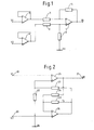
- the two input signals VI and V2 are applied via respective unity gain amplifiers 5 and 6 and respective input resistors 3 and 1 to respective ones of the inverting and non-inverting inputs of an operational amplifier 7.
- a feedback resistor 4 is connected between the output and inverting input of amplifier 7 and a further resistor 2 is connected between its non-inverting input and a common zero-volt reference line for the signals V1 and V2.
- the output signal V0 from amplifier 7 equals (V1 - V2)R4/R3, ie a true differential output is obtained, provided that R4/R3 equals R2/R1 and the open loop differential mode gain of amplifier 7 is very high.
- Each of the unity gain amplifiers 5 and 6 also comprise a high open-loop gain operational amplifier but with a direct feedback connection between its output and inverting input, the signal V1 or V2 as appropriate being applied to the non-inverting input of the amplifier.
- the function of the amplifiers 5 and 6 is to provide a high input impedance to the signals V1 and V2.
- V0 (V2 - V1)R4/R3 but the input impedances seen by the signals V1 and V2 are now relatively low and also unequal, that for V1 being approximately equal to R3 and that for V2 being around (R1 + R2).
- V1 and V2 were derived from sources generating equal emfs and having finite source impedances, then V1 and V2 would become different even if those source impedances were equal, which may well not be the case.
- the input signals V1 and V2 are applied via input terminals 20 direct to the inverting input of an amplifier 25 and the non-inverting input of an amplifier 26 respectively.
- the non-inverting input of amplifier 25 is connected via resistor 22 to a common reference line for signals V1 and V2, again a zero-volt reference in this example, and via a resistor 21 to the output of amplifier 26.
- the inverting input of amplifier 26 is connected via resistor 23 to the output of the same amplifier 26 and vi a resistor 24 to the output of the amplifier 25.
- the circuit output terminal 27 is also connected to the output of the amplifier 25.
- the potential at the non-inverting input of amplifier 25 must equal the potential V1, at its inverting input while the potential at the inverting input of amplifier 26 must equal the potential V2 at the non-inverting input of the amplifier 26. If the potential at the non-inverting input of the amplifier 25 is V1, then the potential at the output of amplifier 26 must be V1(R21 + R22)/R22. Thus, the potential dropped across resistor 23 is defined and hence also the current i3 flowing through it. This current also flows through resistor 24 and hence the voltage drop across it can be calculated and thence also the output voltage V0.
- figure 2 has only two amplifiers instead of three. This not only reduces cost but, in addition, assuming the detailed design is properly done, the circuit of figure 1 can have somewhat superior frequency and offset performance. This is so simply because both these parameters tend to be degraded by the amplifiers of which figure 2 has only two instead of three.
- the amplifiers 25 and 26 in figure 2 each have a high open-loop gain.
- the term 'high' here means at least several times greater than the designed differential mode gain of the circuit, preferably several orders of magnitude greater.
- the relationship between the amplifier open-loop gain and the design differential mode gain determines the accuracy of the circuit, for example if the open-loop gain is one hundred times the differential mode gain of the circuit, then the circuit will have an inherent inaccuracy of around one percent. All this applies equally well to the figure 1 circuit of course and those skilled in the art will be well able to choose appropriate amplifiers.
- the amplifiers 25 and 26 may well be chosen from the range of integrated circuit operational amplifiers, presently commercially available, which have such high open-loop gains that the point becomes somewhat irrelevant.
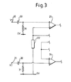
- the circuit shown in figure 2 is especially suitable where the signals V1 and V2 are direct current (d.c.) to low frequency alternating signals. If the circuit is to handle only alternating signals these can be a.c. coupled into the amplifiers 25 and 26 as shown in figure 3.
- the figure 3 circuit is only partly shown but is identical to that of figure 2 except that each terminal 20 is connected to its associated amplifier via a capacitor 30 while in each case a resistor 31 is connected between the zero-volt reference line and the point of interconnection between the capacitor and amplifier
- the relative values of the capacitors 30 and resistors 31 are chosen in dependence upon the input signal frequency range to be handled - the resistors 31, would normally best have quite high values, perhaps one Megaohm or more.
- resistors 21 to 24 could be replaced, by an appropriate impedance network intended for example, to achieve some special frequency characteristic.
- a resistor could be replaced by a resistor and inductor in series, a resistor and a capacitor in parallel, or a combination of these. In this, care has to be taken of course not the render the circuit unstable, ie to turn it into an oscillator circuit.
Abstract
Description
- A previously proposed circuit for the differential amplification of two input signals comprises an operational amplifier with a particular arrangement of feedback and input resistors of which the relative values are such as to achieve a true differential output from the amplifier. In order to achieve a high input impedance for each signal, which is desirable for reasons to be described later herein, the input signals have to be applied to the previously proposed circuit via respective high input impedance unity gain amplifiers. Thus, altogether, three amplifiers are needed which not only incurs a cost penalty but also can limit the obtainable performance.
- The 1986 Linear Applications Databook published by National Semiconductor Corporation shows, on page 90, a proposed circuit for a high input impedance instrumentation amplifier using only two operational amplifiers. The input signals are applied to respective ones of the non-inverting inputs of the two amplifiers; the output signal is taken from the output of one of the amplifiers; and first, second, third and fourth resistors are connected respectively between ground and the inverting input of the other amplifier, between the inverting input and the output of this other amplifier, between the output of this other amplifier and the inverting input of the one amplifier and between the inverting input and the output of the one amplifier. The first and fourth resistors are given equal values while the second and third resistors are also made equal to one another and the differential gain of the arrangement is then determined by the ratio of the first and second resistor values.
- The object of this invention is to provide an alternative configuration for a high input impedance differential amplifier, which alternative may be preferred to the above described prior art proposal, for example to more easily permit the adoption of some particular layout design for an overall integrated circuit which incorporates the differential amplifier.
- According to one aspect of the invention, there is provided a circuit for the differential amplification of a first and a second received signal, the circuit comprising:-
first, second, third and fourth electrical conductor portions for receiving said first signal between the first and third portions and said second signal between the second and third portions, the fourth portion being for supplying an output signal of the circuit;
first and second operational amplifiers each having an inverting input, a non-inverting input and an output, the inverting input of the first amplifier being coupled to said first electrical conductor portion, the non-inverting input of the second amplifier being coupled to said second electrical conductor portion, and the output of the first amplifier being coupled to the fourth electrical conductor portion;
first circuit means defining a resistive path having a first resistance value between the non-inverting input of the first amplifier and the output of the second amplifier;
second circuit means defining a resistive path having a second resistance value between the non-inverting input of the first amplifier and said third electrical conductor portion;
third circuit means defining a resistive path having a third resistance value between the inverting input and output of the second amplifier; and
fourth circuit means defining a resistive path having a fourth resistance value between the output of the first amplifier and the inverting input of the second amplifier;
the ratio of the second to the first resistance value being substantially equal to the ratio of the fourth to the third resistance value. - According to a second aspect of the invention, there is provided differential amplification circuit comprising an amplifier with inverting and non-inverting inputs and an output for supplying the amplified difference between two input signals to the circuit, amplification means for ensuring the presentation of a high input impedance to each of the two input signals, and a plurality of resistors connected to the amplifier and amplification means for ensuring true differential amplification of the two input signals and for defining the gain of the circuit, characterised in that the amplification means comprises a single second amplifier (26) with inverting and non-inverting inputs, said input signals are applied to respective ones of the inverting input of the first mentioned amplifier (25) and the non-inverting input of the second amplifier (26), and said plurality of resistors comprise a first resistor (22) connected between a common ground potential point and the non-inverting input of the first mentioned amplifier, a second resistor (21) between the non-inverting input of the first mentioned amplifier (25) and the output of the second amplifier, a third resistor (24) between the output of the first amplifier (25) and the inverting input of the second amplifier (26), and a fourth resistor (23) between the inverting input and the output of the second amplifier, the ratio (R22/R21) of said second to said first resistor being at least substantially equal to the ratio (R24/R23) of the third to the fourth resistor.
- For a better understanding of the invention, reference will be made, by way of example, to the accompanying drawings, in which:-
- figure 1 is a simplified diagram of a previously proposed differential amplifier circuit,
- figure 2 is a simplified diagram of a differential amplifier circuit in accordance with the present invention, and
- figure 3 is part of a simplified diagram of a modification of the figure 2 circuit, the modification also being in accordance with the present invention.
- In the previously proposed differential amplifier circuit of figure 1, the two input signals VI and V2 are applied via respective
unity gain amplifiers 5 and 6 andrespective input resistors 3 and 1 to respective ones of the inverting and non-inverting inputs of anoperational amplifier 7. A feedback resistor 4 is connected between the output and inverting input ofamplifier 7 and afurther resistor 2 is connected between its non-inverting input and a common zero-volt reference line for the signals V1 and V2. With R1, R2, R3 and R4 being the resistance values of theresistors amplifier 7 equals (V1 - V2)R4/R3, ie a true differential output is obtained, provided that R4/R3 equals R2/R1 and the open loop differential mode gain ofamplifier 7 is very high. Each of theunity gain amplifiers 5 and 6 also comprise a high open-loop gain operational amplifier but with a direct feedback connection between its output and inverting input, the signal V1 or V2 as appropriate being applied to the non-inverting input of the amplifier. The function of theamplifiers 5 and 6 is to provide a high input impedance to the signals V1 and V2. If theamplifiers 5 and 6 were not present, ie if the signals V1 and V2 were to be applied direct to theinput resistors 3 and 1, there would still be obtained an output V0 = (V2 - V1)R4/R3 but the input impedances seen by the signals V1 and V2 are now relatively low and also unequal, that for V1 being approximately equal to R3 and that for V2 being around (R1 + R2). Thus, if V1 and V2 were derived from sources generating equal emfs and having finite source impedances, then V1 and V2 would become different even if those source impedances were equal, which may well not be the case. The result, of course, is that for the two sources producing equal emfs, an output signal is produced byamplifier 7 and this is normally undesirable. The presence of theunity gain amplifiers 5 and 6 avoids the above problems but, of course, the circuit then comprises three operational amplifiers. - In the example, shown in figure 2, of a differential amplifier circuit according to the invention, the input signals V1 and V2 are applied via
input terminals 20 direct to the inverting input of anamplifier 25 and the non-inverting input of anamplifier 26 respectively. The non-inverting input ofamplifier 25 is connected viaresistor 22 to a common reference line for signals V1 and V2, again a zero-volt reference in this example, and via aresistor 21 to the output ofamplifier 26. The inverting input ofamplifier 26 is connected viaresistor 23 to the output of thesame amplifier 26 and viaresistor 24 to the output of theamplifier 25. Thecircuit output terminal 27 is also connected to the output of theamplifier 25. It can be shown by analysis along the lines indicated by the formulae and voltage values given on figure 2, and verified by inspection of the circuit diagram, that the signal V0 at the output of theamplifier 25 equals (V2 - V1)(R21 + R22)/R21, ie a true differential output is again obtained, provided that R24/R23 equals R22/R21, where R21, R22, R23 and R24 are the resistance values ofresistors amplifiers amplifier 25 must equal the potential V1, at its inverting input while the potential at the inverting input ofamplifier 26 must equal the potential V2 at the non-inverting input of theamplifier 26. If the potential at the non-inverting input of theamplifier 25 is V1, then the potential at the output ofamplifier 26 must be V1(R21 + R22)/R22. Thus, the potential dropped acrossresistor 23 is defined and hence also the current i₃ flowing through it. This current also flows throughresistor 24 and hence the voltage drop across it can be calculated and thence also the output voltage V0. - As with the figure 1 circuit, the signals V1 and V2 each see a high input impedance. Meanwhile, however, figure 2 has only two amplifiers instead of three. This not only reduces cost but, in addition, assuming the detailed design is properly done, the circuit of figure 1 can have somewhat superior frequency and offset performance. This is so simply because both these parameters tend to be degraded by the amplifiers of which figure 2 has only two instead of three.
- Just as with the amplifiers of figure 1, it is assumed that the
amplifiers amplifiers - The circuit shown in figure 2 is especially suitable where the signals V1 and V2 are direct current (d.c.) to low frequency alternating signals. If the circuit is to handle only alternating signals these can be a.c. coupled into the
amplifiers terminal 20 is connected to its associated amplifier via acapacitor 30 while in each case aresistor 31 is connected between the zero-volt reference line and the point of interconnection between the capacitor and amplifier The relative values of thecapacitors 30 andresistors 31 are chosen in dependence upon the input signal frequency range to be handled - theresistors 31, would normally best have quite high values, perhaps one Megaohm or more. - Although not always essential, it may be desirable in the case of figure 3 to also provide a.c. coupling at the output side of the circuit, ie by interposing a series capacitor (not shown) between the
amplifier 25 andoutput terminal 27. The capacitor should be downstream of the connection toresistor 24 to avoid upsetting the d.c. state of the circuit. Similarly, provided the d.c. state setting paths between the amplifiers are maintained, one or more of theresistors 21 to 24 could be replaced, by an appropriate impedance network intended for example, to achieve some special frequency characteristic. For example, a resistor could be replaced by a resistor and inductor in series, a resistor and a capacitor in parallel, or a combination of these. In this, care has to be taken of course not the render the circuit unstable, ie to turn it into an oscillator circuit.
Claims (7)
first, second, third and fourth electrical conductor portions for receiving said first signal between the first and third portions and said second signal between the second and third portions, the fourth portion being for supplying an output signal of the circuit;
first and second operational amplifiers each having an inverting input, a non-inverting input and an output, the inverting input of the first amplifier being coupled to said first electrical conductor portion, the non-inverting input of the second amplifier being coupled to said second electrical conductor portion, and the output of the first amplifier being coupled to the fourth electrical conductor portion;
first circuit means defining a resistive path having a first resistance value between the non-inverting input of the first amplifier and the output of the second amplifier;
second circuit means defining a resistive path having a second resistance value between the non-inverting input of the first amplifier and said third electrical conductor portion;
third circuit means defining a resistive path having a third resistance value between the inverting input and output of the second amplifier; and
fourth circuit means defining a resistive path having a fourth resistance value between the output of the first amplifier and the inverting input of the second amplifier;
the ratio of the second to the first resistance value being substantially equal to the ratio of the fourth to the third resistance value.
Applications Claiming Priority (2)
| Application Number | Priority Date | Filing Date | Title |
|---|---|---|---|
| GB8704193 | 1987-02-23 | ||
| GB878704193A GB8704193D0 (en) | 1987-02-23 | 1987-02-23 | Differential amplifier circuit |
Publications (3)
| Publication Number | Publication Date |
|---|---|
| EP0280516A2 true EP0280516A2 (en) | 1988-08-31 |
| EP0280516A3 EP0280516A3 (en) | 1989-05-10 |
| EP0280516B1 EP0280516B1 (en) | 1992-11-11 |
Family
ID=10612760
Family Applications (1)
| Application Number | Title | Priority Date | Filing Date |
|---|---|---|---|
| EP88301549A Expired EP0280516B1 (en) | 1987-02-23 | 1988-02-23 | Differential amplifier circuit |
Country Status (6)
| Country | Link |
|---|---|
| US (1) | US4853644A (en) |
| EP (1) | EP0280516B1 (en) |
| JP (1) | JPS63314009A (en) |
| DE (1) | DE3875754T2 (en) |
| DK (1) | DK168722B1 (en) |
| GB (1) | GB8704193D0 (en) |
Cited By (2)
| Publication number | Priority date | Publication date | Assignee | Title |
|---|---|---|---|---|
| EP0453680A2 (en) * | 1990-04-27 | 1991-10-30 | Analog Devices, Inc. | Three-terminal operational amplifier and applications thereof |
| EP0454972A2 (en) * | 1990-05-03 | 1991-11-06 | Motorola, Inc. | A high gain differential-to single ended amplifier having a tee network feedback loop |
Families Citing this family (1)
| Publication number | Priority date | Publication date | Assignee | Title |
|---|---|---|---|---|
| CN104007353B (en) * | 2013-02-26 | 2016-12-28 | 国网山东省电力公司菏泽供电公司 | Interface testing circuit |
Citations (1)
| Publication number | Priority date | Publication date | Assignee | Title |
|---|---|---|---|---|
| EP0208433A2 (en) * | 1985-07-05 | 1987-01-14 | Robert G. Irvine | Response-gain independent amplifier |
-
1987
- 1987-02-23 GB GB878704193A patent/GB8704193D0/en active Pending
-
1988
- 1988-02-23 DE DE8888301549T patent/DE3875754T2/en not_active Expired - Fee Related
- 1988-02-23 US US07/159,101 patent/US4853644A/en not_active Expired - Fee Related
- 1988-02-23 DK DK094488A patent/DK168722B1/en not_active IP Right Cessation
- 1988-02-23 JP JP63040541A patent/JPS63314009A/en active Pending
- 1988-02-23 EP EP88301549A patent/EP0280516B1/en not_active Expired
Patent Citations (1)
| Publication number | Priority date | Publication date | Assignee | Title |
|---|---|---|---|---|
| EP0208433A2 (en) * | 1985-07-05 | 1987-01-14 | Robert G. Irvine | Response-gain independent amplifier |
Non-Patent Citations (2)
| Title |
|---|
| ELECTRICAL DESIGN NEWS, vol. 31, no. 11, May 1986, pages 185-194,196,198,200, Boston, Massachusetts, US; R. WIDLAR et al.: "High-power op amp provides diverse circuit functions" * |
| IEEE ELECTRO, vol. 7, May 1982, pages 1-13, New York, US; T.J. SCHWARTZ, Sr. et al.: "IC OP AMP combines lowest noise performance available with prevision and high speed" * |
Cited By (4)
| Publication number | Priority date | Publication date | Assignee | Title |
|---|---|---|---|---|
| EP0453680A2 (en) * | 1990-04-27 | 1991-10-30 | Analog Devices, Inc. | Three-terminal operational amplifier and applications thereof |
| EP0453680A3 (en) * | 1990-04-27 | 1991-11-27 | Precision Monolithics Inc. | Three-terminal operational amplifier and applications thereof |
| EP0454972A2 (en) * | 1990-05-03 | 1991-11-06 | Motorola, Inc. | A high gain differential-to single ended amplifier having a tee network feedback loop |
| EP0454972A3 (en) * | 1990-05-03 | 1993-03-31 | Motorola, Inc. | A high gain differential-to single ended amplifier having a tee network feedback loop |
Also Published As
| Publication number | Publication date |
|---|---|
| EP0280516B1 (en) | 1992-11-11 |
| DK94488A (en) | 1988-08-24 |
| JPS63314009A (en) | 1988-12-22 |
| DE3875754D1 (en) | 1992-12-17 |
| DE3875754T2 (en) | 1993-04-22 |
| US4853644A (en) | 1989-08-01 |
| EP0280516A3 (en) | 1989-05-10 |
| DK94488D0 (en) | 1988-02-23 |
| DK168722B1 (en) | 1994-05-24 |
| GB8704193D0 (en) | 1987-04-01 |
Similar Documents
| Publication | Publication Date | Title |
|---|---|---|
| US4320351A (en) | Differential amplifying system with bootstrapping | |
| US4152659A (en) | Low noise differential amplifier | |
| JPH0326563B2 (en) | ||
| US7123080B2 (en) | Differential amplification input circuit | |
| US4227095A (en) | Deviation driver circuit | |
| EP0280516B1 (en) | Differential amplifier circuit | |
| US4217555A (en) | Amplifier circuit arrangement with stabilized power-supply current | |
| US4879521A (en) | Differential amplifier | |
| US5153499A (en) | Precision voltage controlled current source with variable compliance | |
| US4739280A (en) | Amplifier circuit having reduced crossover distortion | |
| US6680642B2 (en) | Analog bipolar current source | |
| EP1088393B1 (en) | Amplifier arrangement | |
| JPS6228606B2 (en) | ||
| EP0492291A1 (en) | Double bridge amplifier stage for two input signals, particularly for stereo applications | |
| JP4839572B2 (en) | Input circuit | |
| US4123721A (en) | Bias current compensated operational amplifier circuit | |
| JP3216753B2 (en) | DA conversion circuit device | |
| RU2054790C1 (en) | Measuring operational amplifier | |
| SU981897A1 (en) | Inductive voltage divider | |
| JP2022060091A (en) | Differential amplifier circuit | |
| NO172019B (en) | Differential gain | |
| JPH0495406A (en) | Differential amplifier circuit | |
| JPH0494203A (en) | Amplifier circuit | |
| JPH10290124A (en) | Electronic circuit | |
| JPS6322666B2 (en) |
Legal Events
| Date | Code | Title | Description |
|---|---|---|---|
| PUAI | Public reference made under article 153(3) epc to a published international application that has entered the european phase |
Free format text: ORIGINAL CODE: 0009012 |
|
| 17P | Request for examination filed |
Effective date: 19880305 |
|
| AK | Designated contracting states |
Kind code of ref document: A2 Designated state(s): CH DE FR GB IT LI SE |
|
| PUAL | Search report despatched |
Free format text: ORIGINAL CODE: 0009013 |
|
| AK | Designated contracting states |
Kind code of ref document: A3 Designated state(s): CH DE FR GB IT LI SE |
|
| 17Q | First examination report despatched |
Effective date: 19911001 |
|
| GRAA | (expected) grant |
Free format text: ORIGINAL CODE: 0009210 |
|
| RAP3 | Party data changed (applicant data changed or rights of an application transferred) |
Owner name: BRITISH AEROSPACE PUBLIC LIMITED COMPANY |
|
| ITF | It: translation for a ep patent filed |
Owner name: BARZANO' E ZANARDO ROMA S.P.A. |
|
| AK | Designated contracting states |
Kind code of ref document: B1 Designated state(s): CH DE FR GB IT LI SE |
|
| REF | Corresponds to: |
Ref document number: 3875754 Country of ref document: DE Date of ref document: 19921217 |
|
| ET | Fr: translation filed | ||
| ITTA | It: last paid annual fee | ||
| PLBE | No opposition filed within time limit |
Free format text: ORIGINAL CODE: 0009261 |
|
| STAA | Information on the status of an ep patent application or granted ep patent |
Free format text: STATUS: NO OPPOSITION FILED WITHIN TIME LIMIT |
|
| 26N | No opposition filed | ||
| PGFP | Annual fee paid to national office [announced via postgrant information from national office to epo] |
Ref country code: FR Payment date: 19950113 Year of fee payment: 8 |
|
| PGFP | Annual fee paid to national office [announced via postgrant information from national office to epo] |
Ref country code: SE Payment date: 19950116 Year of fee payment: 8 |
|
| PGFP | Annual fee paid to national office [announced via postgrant information from national office to epo] |
Ref country code: GB Payment date: 19950119 Year of fee payment: 8 Ref country code: DE Payment date: 19950119 Year of fee payment: 8 Ref country code: CH Payment date: 19950119 Year of fee payment: 8 |
|
| EAL | Se: european patent in force in sweden |
Ref document number: 88301549.7 |
|
| PG25 | Lapsed in a contracting state [announced via postgrant information from national office to epo] |
Ref country code: GB Effective date: 19960223 |
|
| PG25 | Lapsed in a contracting state [announced via postgrant information from national office to epo] |
Ref country code: SE Effective date: 19960224 |
|
| PG25 | Lapsed in a contracting state [announced via postgrant information from national office to epo] |
Ref country code: LI Effective date: 19960229 Ref country code: CH Effective date: 19960229 |
|
| REG | Reference to a national code |
Ref country code: CH Ref legal event code: PL |
|
| GBPC | Gb: european patent ceased through non-payment of renewal fee |
Effective date: 19960223 |
|
| PG25 | Lapsed in a contracting state [announced via postgrant information from national office to epo] |
Ref country code: FR Effective date: 19961031 |
|
| PG25 | Lapsed in a contracting state [announced via postgrant information from national office to epo] |
Ref country code: DE Effective date: 19961101 |
|
| REG | Reference to a national code |
Ref country code: FR Ref legal event code: ST |
|
| PG25 | Lapsed in a contracting state [announced via postgrant information from national office to epo] |
Ref country code: IT Free format text: LAPSE BECAUSE OF NON-PAYMENT OF DUE FEES;WARNING: LAPSES OF ITALIAN PATENTS WITH EFFECTIVE DATE BEFORE 2007 MAY HAVE OCCURRED AT ANY TIME BEFORE 2007. THE CORRECT EFFECTIVE DATE MAY BE DIFFERENT FROM THE ONE RECORDED. Effective date: 20050223 |