EP0279160A2 - Méthode et processeur série à grande vitesse des pixels du voisinnage - Google Patents
Méthode et processeur série à grande vitesse des pixels du voisinnage Download PDFInfo
- Publication number
- EP0279160A2 EP0279160A2 EP88100080A EP88100080A EP0279160A2 EP 0279160 A2 EP0279160 A2 EP 0279160A2 EP 88100080 A EP88100080 A EP 88100080A EP 88100080 A EP88100080 A EP 88100080A EP 0279160 A2 EP0279160 A2 EP 0279160A2
- Authority
- EP
- European Patent Office
- Prior art keywords
- memory
- pixels
- serial
- input
- pixel
- Prior art date
- Legal status (The legal status is an assumption and is not a legal conclusion. Google has not performed a legal analysis and makes no representation as to the accuracy of the status listed.)
- Withdrawn
Links
- 238000000034 method Methods 0.000 title description 6
- 230000015654 memory Effects 0.000 claims abstract description 128
- 238000001914 filtration Methods 0.000 claims description 17
- 230000002401 inhibitory effect Effects 0.000 claims 1
- 230000001360 synchronised effect Effects 0.000 claims 1
- 239000004020 conductor Substances 0.000 description 115
- 238000010586 diagram Methods 0.000 description 8
- 230000004044 response Effects 0.000 description 6
- 230000001934 delay Effects 0.000 description 2
- 230000006870 function Effects 0.000 description 2
- 238000012545 processing Methods 0.000 description 2
- 101100191136 Arabidopsis thaliana PCMP-A2 gene Proteins 0.000 description 1
- 238000012935 Averaging Methods 0.000 description 1
- 101100048260 Saccharomyces cerevisiae (strain ATCC 204508 / S288c) UBX2 gene Proteins 0.000 description 1
- 239000003086 colorant Substances 0.000 description 1
- 230000011664 signaling Effects 0.000 description 1
Images


Classifications
-
- G—PHYSICS
- G06—COMPUTING; CALCULATING OR COUNTING
- G06T—IMAGE DATA PROCESSING OR GENERATION, IN GENERAL
- G06T5/00—Image enhancement or restoration
- G06T5/20—Image enhancement or restoration using local operators
Definitions
- the invention relates to apparatus and methods for receiving high speed serial data arranged in rows from a scanner and performing filtering operations on each pixel based on the states of a neighborhood of pixels surrounding that pixel and serially outputting filtered data or pixels at the same speed.
- serial data arranged in rows to form pages or screens is produced by a serial scanner that scans the rows and outputs the data serially.
- a CCD (charged coupled device) or a video scanner may produce serial pixel data at a 10 MHz rate.
- Each row of scanned data may include, for example, 1000 pixels followed by an "end of row” signal, and after, for example, 1000 rows have been scanned, an "end of page" or end of screen signal may be produced.
- Each pixel code may be a logical "0", representing a light area or a logical "1" indicating a dark area, or each pixel code may be a multi-bit code representing a wide range of colors, from transparent through black.
- noise i.e., extraneous spots or irregularities of the surface or item being scanned. It is very desirable to be able to filter such noise information out of the pixel data.
- a technique for filtering the pixel data involves processing a high speed string of serial pixel codes by feeding them into a high speed computer, and executing filtering algorithms that examine three pixel by three pixel neighborhoods as they would appear on a display screen.
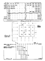
- Fig. 1 shows a simplified screen of data in which P1, P2, P3, etc., represent pixel codes that are serially output.
- each row includes 100 pixels
- each page or screen includes 100 rows, although in many applications there typically would be 3400 pixel codes per row, and 3400 rows per page or screen.
- reference numeral 2 designates a three by three pixel neighborhood centered about a "present" or "object” pixel P ⁇ i.
- the above-mentioned filtering algorithm produces a new filtered value of P ⁇ i based on the values of neighborhood pixels surrounding P ⁇ i within the solid line designating the neighborhood 2.
- the neighborhood 2 shifts one pixel to right, as indicated by the dotted lines 3, and the object pixel would become P ⁇ 5, and its filtered value, based on the eight surrounding neighborhood pixels, would be computed by the filtering algorithm.
- the algorithm takes a suitable weighted average of all nine pixel codes within neighborhood 2. Then, the neighborhood 2 is moved one pixel to the right, as indicated by dotted lines 3, and the filtering algorithm is re-executed for the object pixel in the center of that neighborhood 3. This procedure of shifting the object neighborhood by one pixel and computing a new weighted average for the object pixel thereof is repeated for every incoming pixel code to obtain the filtered pixel code values, which then are serially output to a conventional display memory or the like. The filtered pixel codes then are serially fed from the display memory to a display screen so that a filtered image appears without the above-mentioned extraneous noise images picked up by the scanning apparatus.
- a problem with the above-described technique is that the execution of the filtering algorithm by a computer is very time consuming.
- Each of the nine pixel codes in each neighborhood has to be accessed at least once, and this must be done sequentially, since random access memories need to be accessed one location at a time.
- additional computer instruction cycles are required to execute whatever filtering algorithm is applied to the present neighborhood.
- the invention provides a pixel processor including serially connected first, second, and third memories, and also including fourth, fifth, and sixth serially connected memories, and control circuitry for writing odd numbered rows of pixels into the first memory and even numbered rows of incoming pixels into the fourth memory, and circuitry for shifting odd numbered rows of pixels stored in the first and second memories into the second and third memories, respectively, simultaneously with the writing of even numbered rows of incoming pixels into the second memory.
- circuitry is provided for shifting even numbered rows of pixels stored in the fourth and fifth memories into the fifth and sixth memories, respectively, simultaneously with the writing of odd numbered rows of pixels into the first memory.
- the outputs of the six memories are coupled to inputs of multiplexer circuitry.
- the outputs of the multiplexer circuitry are coupled to the inputs of three three-bit serial-to parallel-converters.
- the three outputs of the first serial-to parallel converter represent the first row of a pixel neighborhood
- the three outputs of the second serial-to-parallel converter represent the second row of the same pixel neighborhood
- the outputs of the third serial-to-parallel converter represent the third row of the same neighborhood.
- the outputs of the three serial-to-parallel converters are gated to address inputs of a read only memory storing filter algorithms. Outputs of the read only memory represent output pixel data that is filtered in accordance with the stored filter algorithms or tables.
- a demultiplexer selects the desired pixel output.
- the apparatus presents the three by three pixel neighborhoods at the same data rate at which input pixels are supplied from a scanner to the device, causing the filtered outputs of the read only memory to also appear at the same data rate. Consequently, the demultiplexed or selected pixel output signal has the same data rate as the pixel inputs.
- Circuitry is provided to inhibit outputting of pixel data until the first and second rows of pixels and the first two pixels of the third row are written into the memories so that the first complete three by three pixel neighborhood is available before outputting of any filtered pixel data. Circuitry also is provided to automatically generate internal strobe signals needed to continue clocking of stored data through the memories after an "end of page" signal is received, allowing neighborhoods still stored in the memories to be filtered and converted to pixel output data.
- Gating circuitry applies logical "0" input levels to the address inputs of the read only memory as necessary to generate "dummy" left-hand columns for neighborhoods in which the object pixel is on the left-hand end of the stored pixel rows, and also includes circuitry for applying logical "0" levels to address inputs of the read only memory to provide a "dummy" right-hand column for neighborhoods of pixels at the right-hand end of the stored rows, allowing accurate filtering of the pixels at the beginning and end of every row.
- Fig. 2 shows a typical three by three pixel neighborhood 2, utilized to determine a weighted average or filtered value of the center or object pixel P ⁇ i.
- the neighborhood 2 moves from left to right so that the center pixel P ⁇ i moves to the right by one pixel, forming a new neighborhood 3, forming a weighted average of the center pixel of the new neighborhood, and repeating the operation until the end of the present row is reached.
- the neighborhood then moves to the beginning of the next row so that P ⁇ i is located at the left or beginning side of the next row.
- FIG. 3 An overview of how the neighborhood processor of the present invention works can be seen by reference to Fig. 3, wherein reference numeral 4 indicates a 10 MHz stream of serial input pixel code data.
- the pixel processor of the present invention produces a sequence of nine bit windows or neighborhoods in the sequence 2A, 2B, 2C, so that all nine pixels of each three by three successive neighborhood are output at the same 10 MHz data rate that the serial pixel data input is received.
- the nine bit memory window output then is utilized to address a read only memory that outputs a filtered pixel (i.e., pixel code) that corresponds to the present nine bit window (i.e., neighborhood) and represents the filtered value of the center pixel of the present or object neighborhood.
- a filtered pixel i.e., pixel code
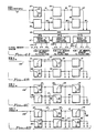
- Fig. 4A discloses a block diagram of the basic components of the neighborhood processor of the present invention.
- Reference numeral 10A designates the conductor on which the pixel data input signal "PIXELS IN" is received from a suitable scanner, such as a document scanner at (for example) at 10 MHz data rate.
- Pixel input conductor 10A is connected to the data input terminal of a first serial memory or memory register circuit 57.
- the data output terminal of memory register 57 is connected by conductor 91 to the data input terminal of a second identical memory register circuit 59 and to an input of a multiplexer circuit 66.
- the data input terminal of memory 59 is connected by conductor 92 to the data input terminal of a third identical memory register circuit 61 and to another input of multiplexer circuit 66.
- the data output terminal of memory 61 is connected by conductor 93 to a third input of multiplexer 66.
- Pixel input conductor 10A also is connected to the data input terminal of a fourth memory register circuit 58, the data output terminal of which is connected by conductor 94 to the data input terminal of a memory register circuit 60 and to a fourth input of multiplexer 66.
- the data output terminal of memory 60 is connected by conductor 95 to the data input terminal of memory 62 and to a fifth input of multiplexer 66 by conductor 95.
- the data output terminal of sixth memory 62 is connected by conductor 96 to the sixth input of multiplexer 66.
- Multiplexer circuit 66 includes three two-input multiplexers, the output of the first multiplexer being connected to conductor 98, the output of the second multiplexer being connected to conductor 99 and the output of the third multiplexer being connected to conductor 100.
- Conductor 98 is connected to the input of a serial-to-parallel converter 67
- conductor 99 is connected to the input of a serial-to-parallel converter 68
- conductor 100 is connected to the input of a serial to parallel converter 69.
- each of the memory register circuits 58-62 is a 16,384 word by one-bit random access memory having a single data input terminal and a single data output terminal.
- Each of the memory circuits 58-62 is connected to address circuitry so that it is operative as a FIFO (first in first out) memory, as explained later with reference to Figs. 5A-5C.
- Each of serial to parallel converters 67-69 is a three bit shift register.
- the result of the operation of the circuit of Fig. 4A is that at any time during operation of the circuit after the first two rows and the first two bits of the third row of pixel data have been written into and shifted into appropriate ones of the memory registers 57-62, the top row of the present neighborhood 2 (Fig. 2) appears at the three outputs of serial-to-parallel converter 69, hereinafter referred to as shift register 69, the middle row of neighborhood 2 appears at the three outputs of shift register 68, and the bottom row of neighborhood 2 appears at the three outputs of shift register 67.
- shift register outputs 101A P ⁇ 1, P ⁇ 2, and P ⁇ 3
- 101B P ⁇ 4, P ⁇ i, and P ⁇ 5
- 101C P ⁇ 6, P ⁇ 7, and P ⁇ 8
- dotted line 110 designates the serial writing of the first row of pixels (Fig. 1) into memory 57.
- the write control input of memory 58 is inhibited during reception of odd numbered rows of pixels on conductor 10A, while the write control input of memory 57 is enabled during the reception of odd numbered rows of pixel on conductor 10A.
- memory 57 has the first row of pixels stored therein.
- an end of row (EOR) signal is received from the scanner.
- EOR end of row
- the first row of pixels 110 is written from memory 57 into second memory 59, as also shown in Fig. 4A. This is accomplished by enabling the write control input of memory 59 and simultaneously addressing memories 57-62.
- Another EOR signal is generated, reversing the write control signals to the two "banks" of memory, the first bank including memories 57, 60, and 61, and the second bank including memories or registers 58, 59, and 63.
- the third row 112 of pixels then is written into first memory 57, as shown by reference numeral 112 in Fig. 4C.
- the second row of pixels 111 is shifted out of fourth memory 58 and into fifth memory 60, as indicated by reference numeral 111 in Fig. 4C, and the first row of pixels 110 is simultaneously shifted out of second memory 59 into third memory 61.
- Another EOR signal is received, reversing the write control operation and resetting the address counting circuitry (described subsequently), and the fourth row 113 of pixels is written into fourth memory 58, while the third row 112 of pixels is shifted from first memory 57 into second memory 59, the second row of pixels 111 is shifted from fifth memory 60 to sixth memory 62, and the first row of pixels 110 is shifted out onto conductor 93.
- multiplexer circuitry 66 and the three three bit serial to parallel shift registers 67-69 is simply to produce, at every new pixel time, a new "snap shot" of the last three pixels output on the three memories that are presently serially outputting pixels stored therein.
- a new three by three pixel neighborhood is produced on conductor groups 101A, 101B, and 101C (Fig. 4A) every pixel time, i.e., at a 10 MHz rate.
- PROM programmable read only memory
- Figs. 5A-5C the detailed structure of the present implementation of the entire neighborhood processor is disclosed, only a portion of which was shown in the block diagram of Fig. 4A.
- five inputs from a suitable scanner include pixel input conductor 10 connected to the D input of a flip-flop or pixel input latch 11, EOR (end of row) conductor 75 connected to the D input of flip-flop 12 and to one input of OR gate 14, EOP IN (end of page) conductor 76 connected to the D input of flip-flop 16, STROBE conductor 77 connected to the trigger input of flip-flop 11, the trigger input of flip-flop 15, the trigger input of flip-flop 16, and one input of OR gate 28, and RESET conductor 78 connected to the input of inverter 23.
- the Q output of pixel input latch 11 is connected to one input of AND gate 13, the output of which produces a PXL IN signal on conductor 10A.
- PXL IN conductor 10A is connected to the data (D) inputs of 16 kilobit random access memories 57 and 58.
- the Q output of end of row latch 12 is connected to EOR conductor 75A.
- the Q output of end of page latch 16 is connected by EOR conductor 76B to the D input of flip-flop 17 and to one input of a two-input NAND gate in 10 MHz oscillator circuit 26.
- the R (reset) inputs of D type flip-flops 11, 12, 16 and all are connected by conductor 78A to the output of inverter 23, wherein the signal RESET* is produced.
- the reset input of D type flip-flop 15 also is connected to conductor 78A, as is the reset input of D type flip-flop 20 and the preset input of D type flip-flop 29.
- Conductor 78A also is connected to one input of two input AND gate 22 and to the reset inputs of D type flip-flops 51, 54, 30, 31, 32, and 33.
- OR gate 14 The output of OR gate 14 is connected to the D input of flip-flop 15, the Q output of which is connected to conductor 118, on which an EORL (end of row latch) signal is produced.
- Conductor 118 is connected to the trigger (T) inputs of octal latches 34 and 35, which capture the "row count", i.e., the number of pixels per row of the scanned document or image, in response to the first EOR signal.
- the Q* output of flip-flop 15 is connected by inverter 21 to conductor 80, on which an (ERR CLR)* signal, which is not related to the concept of the invention, is produced.
- Conductor 118 also is connected to the other input of two input OR gate 14.
- the Q output of D type flip-flop 16 is connected to the D input of flip-flop 17, the Q output of which is connected to the D input of flip-flop 18.
- the Q output of flip-flop 18 is connected to the D input of flip-flop 19, the Q output of which is connected to the D input of end of page latch 20.
- the trigger (T) inputs of flip-flops 18, 19, and 20 and also the trigger input of flip-flop 29 are connected to a (CNTR CLEAR)* (counter clear) signal on conductor 89A, which is connected to the output of inverter 48.
- the Q* output of flip-flop 20 is connected to one input of two input AND gate 22, the output of which is connected to the reset (R) inputs of flip-flops 17, 18, and 19.
- the second input of the two-input NAND gate in oscillator circuit 26 is connected to an RC feedback circuit.
- the output of that NAND gate is connected to the input of inverter 27, the output of which is applied to one input of a two-input OR gate 28.
- the output of OR gate 28 is connected by conductor 77A to one input of write one-shot circuit 24.
- the Q output of write one-shot 24 is connected to both inputs of two-input AND gate 25 by write conductor 77C.
- Conductor 77C is also connected to one input of each of two-input NAND gates 44 and 45.
- the other input of NAND gate 44 is connected by conductor 97 to the Q output of flip-flop 29.
- the other input of NAND gate 45 is connected by conductor 97A to the Q* output of flip-flop 29.
- the Q* output of write one-shot 24 is connected by conductor 77B to the T (trigger) input of flip-flop 17 and applies a WRITE* signal to the T input of counter clear flip-flop 55, to the input of buffer 49, the output of which is connected to buffer 50, the output of which is connected to the T input of flip-flop 51, and also to one input of two-input AND gate 53.
- the D input of flip-flop 29 is connected to the Q* output thereof by conductor 97A.
- NAND gate 44 produces a WRITE ODD signal on conductor 81.
- Conductor 81 is applied to one input of two-input AND gate 46, the output of which produces a CNTR CLK (counter clock) signal on conductor 83, which is connected to the input of inverter 47 and to the "increment" input of counter 40, which can be a 74ALS193 integrated circuit manufactured by various suppliers.
- Inverter 47 produces a SHIFT REG CLK signal on conductor 87, which is connected to the T input of D type flip-flops 32 and 33, and to one input of two-input AND gate 52, the output of which produces an (OUTPUT STROBE)* signal on conductor 77A.
- NAND gate 45 produces a WRITE EVEN signal on conductor 82, which is applied to the other input of two-input AND gate 46.
- inverter 48 is connected by conductor 89 to the output of two-input OR gate 56, which produces a CNTR CLEAR (counter clear) signal on conductor 89.
- Conductor 89 is also connected to the CLR (clear) inputs of address counters 40, 41, 42, and 43.
- One input of OR gate 56 is connected to RESET conductor 77.
- the other input of OR gate 56 is connected to the Q output of flip-flop 55.
- the D input of EOR flip-flop 51 also is connected to EOR conductor 122.
- the Q output of flip-flop 51 is connected to EOR conductor 84, and the Q* output thereof is connected to EOR* conductor 85.
- Flip-flop 30 has its D input connected to +5 volts, its T input connected to EOR conductor 84, and its Q output connected to the D input of flip-flop 31.
- the T input of flip-flop 31 is connected to conductor 84 and its Q output is connected to the D input of flip-flop 32.
- the Q output of flip-flop 32 is connected to the D input of flip-flop 33, the Q output of which is connected to the other input of two-input AND gate 52 and to the other input of two-input AND gate 53.
- EOR conductor 84 also is connected to the D input of flip-flop 54, the T input of which is connected to the output of AND gate 53.
- the Q output of flip-flop 54 is connected to START ROW conductor 88, and its Q* output is connected to the (START ROW)* conductor 88A.
- the CARRY output of counter 40 is connected to the CU (count up) input of an identical counter 41. Its CARRY output is connected to the CU input of counter 42, the CARRY output of which is connected to the CU input of counter 43.
- the four outputs A-D of counters 40, 41, 42, and 43 are connected, respectively, to the B0-B3 inputs of digital comparators 36, 37, 38, and 39 respectively, and are also connected to the 16 D0-D7 inputs of the two octal latches 34 and 35.
- Fourteen of the address counter outputs 90B are connected to 14 address inputs A0-A13 of each of 16K memories 57-62.
- Comparators 36-39 can be a 74LS85 integrated circuits manufactured by various suppliers. Their respective "match,” “greater than,” and “less than” inputs are cascaded, as shown.
- the write control (W*) inputs of each of memories 57, 60, and 61 receive the WRITE ODD signal on conductor 81, while the W* inputs of memories 58, 59, and 62 are connected by conductor 82 to the WRITE EVEN signal.
- the data output terminals Q of memories 57, 59, and 61 are connected by conductors 91, 92 and 93, respectively, to the 1A, 2B, and 3A inputs of multiplexer 66.
- the Q outputs of memories 58, 60, and 62 are connected by conductors 94, 95, and 96, respectively to the 1B, 2A, and 3B inputs of multiplexer 66, which can be a 74LS157 integrated circuit manufactured by various suppliers.
- the select input of multiplexer 66 is connected to conductor 97, which conducts the SEL1 signal produced by flip-flop 29.
- the 1Y, 2Y, and 3Y outputs of multiplexer 66 are connected by conductors 98, 99, and 100 to the serial inputs of three-bit shift registers 67, 68, and 69 respectively, the outputs of which produce the pixel signals P6, P7, P8, P4, X, P5, P1, P2, and P3, respectively.
- These inputs are applied to separate inputs of three two-input AND gates 70A, as shown, and to another group of two-input AND gates 70B, also as shown.
- the other input of each of AND gates 70A is connected to EOR* conductor 75A while the other input of each of AND gates 70B is connected to the START ROW signal on conductor 88A.
- the outputs of AND gates 70A and 70B are connected to the address inputs of programmable read only memory (PROM) 71, which can be a 63S841 integrated circuit manufactured by Monolithic Memories, Inc.
- PROM programmable read only memory
- the P7, X, and P2 outputs of the three-bit shift registers 67, 68, and 69 are connected to the A0-A2 inputs of PROM 71.
- the four outputs of PROM 71 are connected to the four inputs of a demultiplexer 72, which can be a 74LS153 integrated circuit manufactured by various suppliers.
- the selected output which is selected in response to the signals from the D0 and D1 inputs of a computer bus (not shown), received from latch 73, produces the selected one of the four PROM outputs on pixel output conductor 10B.
- Flip-flop 63 and 64 perform an error indicating function that is not related to the concept of the invention.
- Fifty nanosecond delay line 65 delays the output strobe signal produced on conductor 77A by 50 nanoseconds to match the delay through gates 70A, 70B, PROM 71, and demultiplexer 72 so that the output of neighborhood processor circuit of Figs. 5A-5C looks like the outputs of another scanner. This feature enables a plurality of identical devices to be cascaded to produce suitable successive stages of filtering of the pixel output data serially produced on conductor 10B.
- the circuit of Figs. 5A-5C receives the pixel data from conductor 10.
- the pixel data is latched into pixel latch or flip-flop 11 by the STROBE signal on conductor 77, which also latches the EOR pulse into flip-flop 12.
- the STROBE pulse also triggers flip-flop 15 to perform the function of producing the above-mentioned EORL signal on conductor 118 to capture the address count, i.e., the number of pixels per row, in counters 40-43 in latches 34 and 35 at the end of the first rowof pixels.
- the EORL signal also is used as enable to the "compare" inputs of the digital comparators 36-39 to to determine whether the end of a row of pixels has been reached.
- the STROBE pulse also latches in the "end of page" signal EOP IN on conductor 76 into latch 16.
- EOP IN signal on conductor 76 is latched into end of page latch 16. Its Q output on conductor 76B enables the internal 10 MHz clock circuit. Then the STROBE pulse on conductor 77 ceases, but the output of inverter 27 produces a second internally generated strobe signal which continues to be gated through OR gate 28 to conductor 77A, just as the STROBE signal on conductor 77 was prior to the EOP IN signal.
- the above-mentioned alternating of the writing and readout operations between the first memory bank 57, 59, 61 and the second memory bank 58, 60, 62 is performed in response to the WRITE signal on conductor 77C as a result of a CNTR CLEAR signal on conductor 89, which is inverted by inverter 48 and applied by conductor 89A to the T input of flip-flop 29, which switches state each time an end of row condition is detected by comparators 36-39. Every time either a WRITE ODD or a WRITE EVEN pulse appears on conductor 81 or 82, a CNTR CLK signal appears on conductor 83, generating the SHIFT REG CLK signal on conductor 87.
- the EOR signal on conductor 122 is produced by the output of comparator 39. This generates the EOR signal on conductor 84 and also causes flip-flop 55 and OR gate 56 to generate the CNTR CLEAR signal on conductor 89.
- the CNTR CLK signal on conductor 83 causes all of the address counters 40-43 to be continually incremented at the STROBE rate (see Figs. 6A and 6B) until the end of row count stored in latches 34 and 35 is again attained, signaling the end of scanning of the present row of pixels and beginning scanning of the next row.
- the address counters 40-43 all initially store logical "0"s. Each successive STROBE pulse causes a new WRITE pulse to be produced, and in response to that, a new CNTR CLK pulse is produced. The CNTR CLK pulse then increments the address of the memory counters 40-43.
- the EORL signal is produced on conductor 118 "capturing" the count of all of the address counters 40-43 in the corresponding count latches 34 and 35. This happens only once, because the EORL signal on conductor 118 then disables the D input of flip-flop 15 by means of OR gate 14.
- the EOR signal generated by digital comparator 39 on conductor 122 by the match at the A and B inputs of the comparators 36-39 generates the CNTR CLEAR signal that resets address counters 40-43 at the end of the first row of pixels.
- the WRITE ODD signal on conductor 81 goes to a "0" and the WRITE EVEN signal on conductor 82 goes to a "1", causing the next row of pixels to be written into memory 58, instead of memory 57, and also enables the above described transfers by enabling the second bank of memories 58, 59, and 62, as previously explained.
- the EOR* signal on conductor 75A causes AND gates 70A to produce logical "0"s on the P1, P4, and P6 inputs of the PROM 71.
- the two flip-flops 30 and 31 produce logical "1"s at their outputs in response to the first and second EOR signals received on conductor 84, respectively. This prevents any (OUTPUT STROBE)* signals from being produced on conductor 77A until the first two rows of pixels have been loaded into memories 57-62.
- Flip-flops 32 and 33 add two more pixel delays to allow loading of the first and second pixels of the third row into the memory. As the third pixel of the third row is loaded into the memories, the (OUTPUT STROBE)* signal on conductor 77A begins to occur as the first available neighborhood of the scanned pixel data (including the left-hand dummy column) now has been loaded into the memory.
Landscapes
- Physics & Mathematics (AREA)
- General Physics & Mathematics (AREA)
- Engineering & Computer Science (AREA)
- Theoretical Computer Science (AREA)
- Image Processing (AREA)
- Picture Signal Circuits (AREA)
- Image Input (AREA)
- Facsimile Image Signal Circuits (AREA)
Applications Claiming Priority (2)
| Application Number | Priority Date | Filing Date | Title |
|---|---|---|---|
| US07/016,230 US4797806A (en) | 1987-02-19 | 1987-02-19 | High speed serial pixel neighborhood processor and method |
| US16230 | 1987-02-19 |
Publications (2)
| Publication Number | Publication Date |
|---|---|
| EP0279160A2 true EP0279160A2 (fr) | 1988-08-24 |
| EP0279160A3 EP0279160A3 (fr) | 1990-12-05 |
Family
ID=21776048
Family Applications (1)
| Application Number | Title | Priority Date | Filing Date |
|---|---|---|---|
| EP19880100080 Withdrawn EP0279160A3 (fr) | 1987-02-19 | 1988-01-05 | Méthode et processeur série à grande vitesse des pixels du voisinnage |
Country Status (6)
| Country | Link |
|---|---|
| US (1) | US4797806A (fr) |
| EP (1) | EP0279160A3 (fr) |
| JP (1) | JPH0833923B2 (fr) |
| AU (1) | AU590148B2 (fr) |
| CA (1) | CA1286380C (fr) |
| IL (1) | IL84646A0 (fr) |
Families Citing this family (17)
| Publication number | Priority date | Publication date | Assignee | Title |
|---|---|---|---|---|
| US4821336A (en) * | 1987-02-19 | 1989-04-11 | Gtx Corporation | Method and apparatus for simplifying runlength data from scanning of images |
| US4949388A (en) * | 1987-02-19 | 1990-08-14 | Gtx Corporation | Method and apparatus for recognition of graphic symbols |
| WO1990001750A1 (fr) * | 1988-08-02 | 1990-02-22 | Sorex Corporation | Processeur d'images a balayage intelligent |
| US5195182A (en) * | 1989-04-03 | 1993-03-16 | Eastman Kodak Company | Frame buffer architecture for storing sequential data in alternating memory banks |
| US5263099A (en) * | 1989-11-17 | 1993-11-16 | Picker International, Inc. | High speed window and level function modification for real time video processing |
| US5041912A (en) * | 1990-01-18 | 1991-08-20 | International Business Machines Corporation | Averaging array for CCD imagers |
| US5031227A (en) * | 1990-09-27 | 1991-07-09 | Loral Aerospace Corp. | Edge enhancement and smoothing in digital images |
| US5216725A (en) * | 1990-10-31 | 1993-06-01 | Environmental Research Institute Of Michigan | Apparatus and method for separating handwritten characters by line and word |
| US5062142A (en) * | 1990-12-14 | 1991-10-29 | General Electric Company | Data processor producing a medial axis representation of an extended region |
| US5142589A (en) * | 1990-12-21 | 1992-08-25 | Environmental Research Institute Of Michigan | Method for repairing images for optical character recognition performing different repair operations based on measured image characteristics |
| US5261012A (en) * | 1992-05-11 | 1993-11-09 | General Electric Company | Method and system for thinning images |
| AU705713B2 (en) * | 1995-03-03 | 1999-05-27 | Arch Development Corporation | Method and system for the detection of lesions in medical images |
| US5860086A (en) * | 1995-06-07 | 1999-01-12 | International Business Machines Corporation | Video processor with serialization FIFO |
| DE69623253D1 (de) * | 1996-03-07 | 2002-10-02 | St Microelectronics Srl | Verarbeitungsanordnung für Videosignale |
| US6064497A (en) * | 1996-03-08 | 2000-05-16 | Intel Corporation | Low cost digital scanners |
| US6118789A (en) * | 1998-02-19 | 2000-09-12 | Micron Technology, Inc. | Method of addressing messages and communications system |
| US6038352A (en) * | 1997-10-17 | 2000-03-14 | Acuity Imaging, Llc | Two-bit morphology processing apparatus and method |
Citations (2)
| Publication number | Priority date | Publication date | Assignee | Title |
|---|---|---|---|---|
| US4084196A (en) * | 1977-01-31 | 1978-04-11 | Dacom, Inc. | Electronic half-tone generating means for facsimile reproduction system |
| US4414685A (en) * | 1979-09-10 | 1983-11-08 | Sternberg Stanley R | Method and apparatus for pattern recognition and detection |
Family Cites Families (18)
| Publication number | Priority date | Publication date | Assignee | Title |
|---|---|---|---|---|
| US3737855A (en) * | 1971-09-30 | 1973-06-05 | Ibm | Character video enhancement system |
| US4506301A (en) * | 1979-10-12 | 1985-03-19 | Xerox Corporation | Multiple mode raster scanner |
| US4363104A (en) * | 1980-09-22 | 1982-12-07 | Hughes Aircraft Company | Imaging system having multiple image copying and hierarchical busing |
| US4389677A (en) * | 1980-12-08 | 1983-06-21 | Ncr Canada Ltd - Ncr Canada Ltee | Method and apparatus for removing erroneous elements from digital images |
| US4398256A (en) * | 1981-03-16 | 1983-08-09 | Hughes Aircraft Company | Image processing architecture |
| JPS57178486A (en) * | 1981-04-25 | 1982-11-02 | Nippon Kogaku Kk <Nikon> | Smoothing device for binary image signal |
| JPS6053349B2 (ja) * | 1981-06-19 | 1985-11-25 | 株式会社日立製作所 | 画像処理プロセツサ |
| US4426629A (en) * | 1981-12-24 | 1984-01-17 | Hughes Aircraft Company | Two-dimensional kernel generator for transversal filters |
| US4484349A (en) * | 1982-03-11 | 1984-11-20 | Environmental Research Institute Of Michigan | Parallel pipeline image processor |
| US4499597A (en) * | 1982-03-29 | 1985-02-12 | Hughes Aircraft Company | Small-object location utilizing centroid accumulation |
| US4499598A (en) * | 1982-07-02 | 1985-02-12 | Conoco Inc. | Edge and line detection in multidimensional noisey, imagery data |
| US4496985A (en) * | 1982-07-21 | 1985-01-29 | General Electric Company | Line-locked digital fluorography system |
| US4510618A (en) * | 1982-12-27 | 1985-04-09 | Ncr Canada Ltd - Ncr Canada Ltee | Noise cleaner for binary images |
| US4669043A (en) * | 1984-02-17 | 1987-05-26 | Signetics Corporation | Memory access controller |
| US4698666A (en) * | 1985-07-12 | 1987-10-06 | The Grass Valley Group, Inc. | Video key glow and border generator |
| US4720780A (en) * | 1985-09-17 | 1988-01-19 | The Johns Hopkins University | Memory-linked wavefront array processor |
| US4691233A (en) * | 1986-09-30 | 1987-09-01 | Rca Corporation | Rate buffer control of difference signal decimation and interpolation for adaptive differential pulse code modulator |
| US4706260A (en) * | 1986-11-07 | 1987-11-10 | Rca Corporation | DPCM system with rate-of-fill control of buffer occupancy |
-
1987
- 1987-02-19 US US07/016,230 patent/US4797806A/en not_active Expired - Lifetime
- 1987-11-27 IL IL84646A patent/IL84646A0/xx unknown
- 1987-12-17 CA CA000554657A patent/CA1286380C/fr not_active Expired - Lifetime
-
1988
- 1988-01-05 EP EP19880100080 patent/EP0279160A3/fr not_active Withdrawn
- 1988-01-11 JP JP63003654A patent/JPH0833923B2/ja not_active Expired - Lifetime
- 1988-02-16 AU AU11763/88A patent/AU590148B2/en not_active Ceased
Patent Citations (2)
| Publication number | Priority date | Publication date | Assignee | Title |
|---|---|---|---|---|
| US4084196A (en) * | 1977-01-31 | 1978-04-11 | Dacom, Inc. | Electronic half-tone generating means for facsimile reproduction system |
| US4414685A (en) * | 1979-09-10 | 1983-11-08 | Sternberg Stanley R | Method and apparatus for pattern recognition and detection |
Non-Patent Citations (1)
| Title |
|---|
| COMPUTER VISION, GRAPHICS AND IMAGE PROCESSING, vol. 27, no. 1, July 1984, pages 115-123, NY, US; F.A. GERRITSEN et al.: "Implementation of cellular-logic operators using 3*3 convolution and table lookup hardware" * |
Also Published As
| Publication number | Publication date |
|---|---|
| IL84646A0 (en) | 1988-04-29 |
| EP0279160A3 (fr) | 1990-12-05 |
| US4797806A (en) | 1989-01-10 |
| JPH0833923B2 (ja) | 1996-03-29 |
| AU590148B2 (en) | 1989-10-26 |
| CA1286380C (fr) | 1991-07-16 |
| JPS63223881A (ja) | 1988-09-19 |
| AU1176388A (en) | 1988-10-06 |
Similar Documents
| Publication | Publication Date | Title |
|---|---|---|
| US4797806A (en) | High speed serial pixel neighborhood processor and method | |
| EP0012173B1 (fr) | Appareil pour le traitement d'images à conversion de résolution | |
| US4464789A (en) | Image analyzer for processing multiple frames of image data | |
| US4450483A (en) | Circuit for improving the quality of digitized line images | |
| EP0154449B1 (fr) | Système d'amincissement de caractères en temps réel | |
| US4791677A (en) | Image signal processor | |
| US4442542A (en) | Preprocessing circuitry apparatus for digital data | |
| US20030193593A1 (en) | X-y addressable CMOS APS with compact pixel pitch | |
| US4503469A (en) | Picture image enlarging/reducing system | |
| US3686631A (en) | Compressed coding of digitized quantities | |
| US4454600A (en) | Parallel cyclic redundancy checking circuit | |
| EP0213189B1 (fr) | Procede et appareil d'adaptation de la resolution de documents | |
| US4845767A (en) | Image signal processor | |
| EP0317218A2 (fr) | Processeur vidéo série et processeur vidéo série à tolérance | |
| US4736438A (en) | Image processing device for the real-time processing and recognition of two-dimensional images, and an image processing system including at least two series-connected image processing devices of this kind | |
| US4298858A (en) | Method and apparatus for augmenting binary patterns | |
| US4809343A (en) | Maximum/minimum value conversion circuit for image processing | |
| US5062142A (en) | Data processor producing a medial axis representation of an extended region | |
| GB1598596A (en) | Apparatus for producing electrical signals representing black and white areas of an optically scanned surface | |
| US4153944A (en) | Method and arrangement for buffering data | |
| EP0365878B1 (fr) | Méthode de traitement d'image | |
| JPS5947394B2 (ja) | 可変長二次元シストレジスタ | |
| JPS603715B2 (ja) | 可変長シフトレジスタ | |
| SU1297213A1 (ru) | Цифровой фильтр | |
| JPH0750504B2 (ja) | パタ−ン認識装置 |
Legal Events
| Date | Code | Title | Description |
|---|---|---|---|
| PUAI | Public reference made under article 153(3) epc to a published international application that has entered the european phase |
Free format text: ORIGINAL CODE: 0009012 |
|
| AK | Designated contracting states |
Kind code of ref document: A2 Designated state(s): DE FR GB |
|
| PUAL | Search report despatched |
Free format text: ORIGINAL CODE: 0009013 |
|
| AK | Designated contracting states |
Kind code of ref document: A3 Designated state(s): DE FR GB |
|
| STAA | Information on the status of an ep patent application or granted ep patent |
Free format text: STATUS: THE APPLICATION IS DEEMED TO BE WITHDRAWN |
|
| 18D | Application deemed to be withdrawn |
Effective date: 19910606 |