EP0276902A1 - Verfahren zum Herstellen eines Feldeffekttransistors - Google Patents
Verfahren zum Herstellen eines Feldeffekttransistors Download PDFInfo
- Publication number
- EP0276902A1 EP0276902A1 EP88300021A EP88300021A EP0276902A1 EP 0276902 A1 EP0276902 A1 EP 0276902A1 EP 88300021 A EP88300021 A EP 88300021A EP 88300021 A EP88300021 A EP 88300021A EP 0276902 A1 EP0276902 A1 EP 0276902A1
- Authority
- EP
- European Patent Office
- Prior art keywords
- layer
- substrate
- metallization layer
- nitrogen
- implanted
- Prior art date
- Legal status (The legal status is an assumption and is not a legal conclusion. Google has not performed a legal analysis and makes no representation as to the accuracy of the status listed.)
- Ceased
Links
Images

Classifications
-
- H—ELECTRICITY
- H10—SEMICONDUCTOR DEVICES; ELECTRIC SOLID-STATE DEVICES NOT OTHERWISE PROVIDED FOR
- H10D—INORGANIC ELECTRIC SEMICONDUCTOR DEVICES
- H10D30/00—Field-effect transistors [FET]
- H10D30/01—Manufacture or treatment
- H10D30/061—Manufacture or treatment of FETs having Schottky gates
- H10D30/0612—Manufacture or treatment of FETs having Schottky gates of lateral single-gate Schottky FETs
- H10D30/0616—Manufacture or treatment of FETs having Schottky gates of lateral single-gate Schottky FETs using processes wherein the final gate is made before the completion of the source and drain regions, e.g. gate-first processes
-
- H—ELECTRICITY
- H01—ELECTRIC ELEMENTS
- H01L—SEMICONDUCTOR DEVICES NOT COVERED BY CLASS H10
- H01L21/00—Processes or apparatus adapted for the manufacture or treatment of semiconductor or solid state devices or of parts thereof
- H01L21/02—Manufacture or treatment of semiconductor devices or of parts thereof
- H01L21/04—Manufacture or treatment of semiconductor devices or of parts thereof the devices having potential barriers, e.g. a PN junction, depletion layer or carrier concentration layer
- H01L21/18—Manufacture or treatment of semiconductor devices or of parts thereof the devices having potential barriers, e.g. a PN junction, depletion layer or carrier concentration layer the devices having semiconductor bodies comprising elements of Group IV of the Periodic Table or AIIIBV compounds with or without impurities, e.g. doping materials
- H01L21/28—Manufacture of electrodes on semiconductor bodies using processes or apparatus not provided for in groups H01L21/20 - H01L21/268
- H01L21/283—Deposition of conductive or insulating materials for electrodes conducting electric current
- H01L21/285—Deposition of conductive or insulating materials for electrodes conducting electric current from a gas or vapour, e.g. condensation
- H01L21/28506—Deposition of conductive or insulating materials for electrodes conducting electric current from a gas or vapour, e.g. condensation of conductive layers
- H01L21/28575—Deposition of conductive or insulating materials for electrodes conducting electric current from a gas or vapour, e.g. condensation of conductive layers on semiconductor bodies comprising AIIIBV compounds
- H01L21/28581—Deposition of Schottky electrodes
-
- H—ELECTRICITY
- H01—ELECTRIC ELEMENTS
- H01L—SEMICONDUCTOR DEVICES NOT COVERED BY CLASS H10
- H01L21/00—Processes or apparatus adapted for the manufacture or treatment of semiconductor or solid state devices or of parts thereof
- H01L21/02—Manufacture or treatment of semiconductor devices or of parts thereof
- H01L21/04—Manufacture or treatment of semiconductor devices or of parts thereof the devices having potential barriers, e.g. a PN junction, depletion layer or carrier concentration layer
- H01L21/18—Manufacture or treatment of semiconductor devices or of parts thereof the devices having potential barriers, e.g. a PN junction, depletion layer or carrier concentration layer the devices having semiconductor bodies comprising elements of Group IV of the Periodic Table or AIIIBV compounds with or without impurities, e.g. doping materials
- H01L21/28—Manufacture of electrodes on semiconductor bodies using processes or apparatus not provided for in groups H01L21/20 - H01L21/268
- H01L21/283—Deposition of conductive or insulating materials for electrodes conducting electric current
- H01L21/285—Deposition of conductive or insulating materials for electrodes conducting electric current from a gas or vapour, e.g. condensation
- H01L21/28506—Deposition of conductive or insulating materials for electrodes conducting electric current from a gas or vapour, e.g. condensation of conductive layers
- H01L21/28575—Deposition of conductive or insulating materials for electrodes conducting electric current from a gas or vapour, e.g. condensation of conductive layers on semiconductor bodies comprising AIIIBV compounds
- H01L21/28587—Deposition of conductive or insulating materials for electrodes conducting electric current from a gas or vapour, e.g. condensation of conductive layers on semiconductor bodies comprising AIIIBV compounds characterised by the sectional shape, e.g. T, inverted T
-
- H—ELECTRICITY
- H10—SEMICONDUCTOR DEVICES; ELECTRIC SOLID-STATE DEVICES NOT OTHERWISE PROVIDED FOR
- H10D—INORGANIC ELECTRIC SEMICONDUCTOR DEVICES
- H10D30/00—Field-effect transistors [FET]
- H10D30/60—Insulated-gate field-effect transistors [IGFET]
- H10D30/67—Thin-film transistors [TFT]
- H10D30/6729—Thin-film transistors [TFT] characterised by the electrodes
- H10D30/6737—Thin-film transistors [TFT] characterised by the electrodes characterised by the electrode materials
- H10D30/6738—Schottky barrier electrodes
-
- H—ELECTRICITY
- H10—SEMICONDUCTOR DEVICES; ELECTRIC SOLID-STATE DEVICES NOT OTHERWISE PROVIDED FOR
- H10D—INORGANIC ELECTRIC SEMICONDUCTOR DEVICES
- H10D30/00—Field-effect transistors [FET]
- H10D30/60—Insulated-gate field-effect transistors [IGFET]
- H10D30/67—Thin-film transistors [TFT]
- H10D30/674—Thin-film transistors [TFT] characterised by the active materials
- H10D30/675—Group III-V materials, Group II-VI materials, Group IV-VI materials, selenium or tellurium
-
- H—ELECTRICITY
- H10—SEMICONDUCTOR DEVICES; ELECTRIC SOLID-STATE DEVICES NOT OTHERWISE PROVIDED FOR
- H10D—INORGANIC ELECTRIC SEMICONDUCTOR DEVICES
- H10D62/00—Semiconductor bodies, or regions thereof, of devices having potential barriers
- H10D62/80—Semiconductor bodies, or regions thereof, of devices having potential barriers characterised by the materials
- H10D62/85—Semiconductor bodies, or regions thereof, of devices having potential barriers characterised by the materials being Group III-V materials, e.g. GaAs
-
- H10D64/0124—
-
- H10D64/0125—
-
- H—ELECTRICITY
- H10—SEMICONDUCTOR DEVICES; ELECTRIC SOLID-STATE DEVICES NOT OTHERWISE PROVIDED FOR
- H10D—INORGANIC ELECTRIC SEMICONDUCTOR DEVICES
- H10D64/00—Electrodes of devices having potential barriers
- H10D64/60—Electrodes characterised by their materials
- H10D64/64—Electrodes comprising a Schottky barrier to a semiconductor
-
- Y—GENERAL TAGGING OF NEW TECHNOLOGICAL DEVELOPMENTS; GENERAL TAGGING OF CROSS-SECTIONAL TECHNOLOGIES SPANNING OVER SEVERAL SECTIONS OF THE IPC; TECHNICAL SUBJECTS COVERED BY FORMER USPC CROSS-REFERENCE ART COLLECTIONS [XRACs] AND DIGESTS
- Y10—TECHNICAL SUBJECTS COVERED BY FORMER USPC
- Y10S—TECHNICAL SUBJECTS COVERED BY FORMER USPC CROSS-REFERENCE ART COLLECTIONS [XRACs] AND DIGESTS
- Y10S148/00—Metal treatment
- Y10S148/105—Masks, metal
Definitions
- This invention relates to gallium arsenide (GaAs) field-effect transistors (FETs) and to methods of making such transistors. More particularly, this invention is concerned with a method of making self-aligned gate (SAG) GaAs transistors for use in the integrated circuit field.
- GaAs gallium arsenide
- FETs field-effect transistors
- SAG self-aligned gate
- the process currently being used fall into two categories: (1) Thermally-Stable Refractory Gate (RG), and (2) Substitutional Gate (SG). From a processing standpoint, the RG process is simpler and easier to manufacture than the SG process, but it places stringent requirements on the thermal stability of the Schottky gate metallization. The SG approach places no unusual thermal stability requirements on the gate metal but does require the difficult formation of a tri-layer gate substitution mask with a carefully controlled T-shaped profile.
- RG Thermally-Stable Refractory Gate
- SG Substitutional Gate
- the RG approach may be superior overall to the SG approach, previous embodiments of the RG approach have suffered from the need to compromise some aspects of the process due to inadequate technology.
- gold is used as the refractory metal since it exhibits low resistivity and its thermal stability is sufficient for that process.
- the refractory metals used must be such that they can achieve the necessary thermal stability of the gate Schottky contact. Gold is not a suitable metal for this process.
- a major problem in the past has been the high resistivity of the refractory metals suitable for the RG process relative to that of gold.
- the high resistivity of the refractory gate metallization complicates the RG approach in that the first level interconnect metal, which must have lower resistivity than possible with a refractory metal, is defined by an additional mask level rather than the gate mask level as in the SG process. Also the high gate resistance degrades the performance of RG processed FETs, which precludes using this highly beneficial process to fabricate analog circuits.
- the present invention seeks to provide a self-aligned gate type GaAs field-effect transistor which overcomes the disadvantages of the previously mentioned prior art.
- a process for making a field-effect transistor including the heating of a gallium arsenide substrate having ions implanted therein, characterised in the forming of a gate metallization layer on the substrate which layer is fabricated from titanium-tungsten nitride (TiWN X ) and used as a diffusion barrier for said transistor.
- TiWN X titanium-tungsten nitride
- a method of making field-effect transistor of the self-aligned gate type characterised in the steps of performing a first ion implant in at least one region of a gallium arsenide substrate forming a titanium-tungsten nitride (TiWN X ) metallization layer on the implanted substrate, depositing a gold masking layer on the metallization layer in the implanted region, removing that portion of the metallization layer which is unmasked, performing a self-aligned second implant of ions into the first implanted regions which are the unmasked regions while retaining the gold masking layer, annealing the substrate to activate the implanted regions.
- TiWN X titanium-tungsten nitride
- the invention may provide a refractory gate metallization which simultaneously provides both a high-temperature stable Schottky barrier and an equally high-temperature stable diffusion barrier to gold (Au).
- the use of gold as an etch mask to fabricate a T-gate structure for use as a self-aligned implantation mask and leave the gold in place during an n+ activation anneal can advantageously reduce the gate resistance of the FET. (This precludes the current step of removing the Ni etch mask before the n+ anneal, and so it reduces the number of processing steps.)
- the refractory metal/Au layered metal may be used for both the gate metal and first-level interconnect metal. This increases the throughput of GaAs ICs and reduces the cost of fabrication.
- the present invention may improve the performance of GaAs FETs fabricated using the RG approach by reducing the gate resistance. This permits the highly efficient RG process to the fabrication of analog FETs and MMICS.
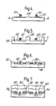
- FIG. 1 there is shown the structure of a self-aligned gate field-effect transistor 10.
- a gallium arsenide (GaAs) substrate 12 is initially cleaned in solvents and then etched to remove that portion of the substrate 12 which may have been damaged by the use of a mechanical slurry polishing process. It has been found that by removing at least approximately 5 ⁇ m from each of the substrate surfaces the damaged portion will be removed and improved electrical properties will result. A problem in removing the material from the substrate is that a pitted or rough-textured surface may result with certain etchants.
- a preferred etchant which avoids this problem is a mixture of sulphuric acid, hydrogen peroxide and water (H2SO4:H2O2:H2O) in a ratio of 5:1:1, used at a temperature in the range of approximately 30° - 40° C.
- This etchant does not damage the wafer 11 and leaves a smooth finish on the surfaces of the wafer 11 which aids in further processing of the wafer, especially when performing photolithography.
- the preferred materials for the dielectric layer 14 are silicon nitride (SiN), silicon oxy-nitride (SiON) or silicon dioxide (Sio2).
- the formation of the dielectric layer 14 protects the substrate surface by isolating it from photoresist residues during later processing.
- the dielectric layer 14 may, however, be eliminated so that ion implants are made directly into the bare GaAs surface.
- a photoresist layer 16 is formed on one surface 15 of the dielectric layer 14.
- the photoresist layer 16 is patterned for registration marks 13 which will serve to align masks on the wafer 11 for patterning implant areas later in the process.
- the pattern of registration marks 13 are etched into the dielectric layer 14 and then into the underlying GaAs substrate 12. After etching, the photoresist layer 16 is removed, preferably with an oxygen plasma.
- photoresist layer 18 is formed on the surface 15 as shown in Figure 3.
- the photoresist layer 18 is patterned to form one or more windows 17 for selective ion implantation through the dielectric layer 14 into the underlying GaAs substrate 12. Patterning is performed in any known manner. Typically, a photographic mask having the desired pattern is positioned on the photoresist layer 18, aligning registration marks on the mask with the registration marks on the substrate 12. The photoresist 18 is exposed to light through the mask, and then the mask is removed. A solvent is applied so that the exposed areas of the resist are dissolved and washed away and the unexposed resist remains to serve as an implant mask.
- the ion implantation step is performed in any known manner.
- the wafer 11 is supported in a vacuum chamber and a beam of ions is uniformly swept over it and implanted into the GaAs substrate 12 through the window 17.
- the implanted region is indicated at 19.
- the material of the dielectric layer 14 has an amorphous structure, thus minimizing planer channeling effects of the arriving ions through the layer 14. If somewhat steeper implant profiles are desired, the dielectric layer 14 may be eliminated and the implant made directly into the GaAs substrate 12. After the implant is performed, the photoresist layer 18 is removed in an oxygen plasma.
- Additional selective implant steps may be performed by forming another photoresist layer on top of the dielectric layer 14, patterning the photoresist layer to form window areas and implanting the desired material through the window area into the dielectric layer 14 and into the GaAs substrate 12.
- the photoresist layer 18 is thereafter removed.
- active and passive devices can be fabricated on the same wafer, for example, enhancement-mode and depletion-mode FETs, diodes and resistors.
- the dielectric layer 14 is removed in hydrogen fluoride (HF).
- a metallization layer 20 is formed on a surface 26 which is the implanted surface of the wafer 11.
- the metallization layer 20 is formed of titanium-tungsten nitride (TiWN X ). This layer 20 differs from the metal layer 20 of the copending application. In that application the layer 20 was formed by the sputter deposition of titanium-tungsten to a depth of 2000 ⁇ .
- One method of formation of the layer 20 is accomplished by reactively sputtering a TiW (30 atomic percent Ti) target in a nitrogen/argon plasma.
- the metallization layer 20 acts as a diffusion barrier between a gold layer, which will be deposited on the metallization layer during subsequent processing, and the gallium arsenide substrate 12.
- a N.(N + Ar) flow ratio of 1/4 is preferred, but a range of 1/10 to 1/1 will also be adequate. By maintaining the nitrogen ratio in this range, an atomic percent of nitrogen results which enables the metallization layer 20 to withstand a subsequent annealing step of approximately 850° C for at least 20 minutes without breakdown of its barrier function.
- the next step in wafer processing is the patterning of the gate structures 24 which begins with the formation of another masking level on the TiWN X layer 20.
- This masking level is a metal etch mask 22 fabricated from gold and formed by liftoff in the following manner.
- a high resolution positive photoresist mask is positioned on top of the TiWN X layer 20.
- the positive photoresist mask has openings which define the regions where a metal is to be deposited which will form the etch mask 22.
- the metal for the etch mask 22 is evaporated on the positive photoresist mask in such a manner that the openings in the mask are filled. After evaporation, the photoresist mask is lifted off and the metallization remaining on the TiWN X layer 20 defines the metal etch mask 22.
- the preferred material for the etch mask 22 is gold and the metal etch mask 22 is not removed but remains in place whereby it greatly reduces the resistance of the gate.
- the underlying TiWN X layer 20 is then reactive-ion etched, using the metal mask 22, in a fluorine-based plasma.
- the plasma will etch the layer 20 in the regions not covered by the metal etch mask 22 and will also undercut the masked region to form T-shaped gate structures 24 as shown in Figure 4.
- the amount of plasma undercut can be controlled by varying the plasma etch parameters. This can be accomplished by initially etching at low pressure to set an anisotropic profile, then increasing the pressure to achieve a faster plasma undercut.
- a photoresist mask 28 is formed on the surface 26 to define regions 29 for self-aligned ion implant.
- self-aligned is used since the mask 22 acts as a barrier to ion implantation by an ion beam and thus defines the limits of heavily doped regions in the substrate.
- n-type doping levels are used for the initial channel implant at a level which will form good Schottky contact, much higher levels of doping (n+) are used during this implant step to facilitate ohmic contact.
- p and p+ implants may be used for Schottky contact and ohmic contact, respectively, n-type doping permits much faster carrier transport.
- the photoresist mask 28 is formed by depositing a layer of a positive photoresist on the wafer 11 and exposing the photoresist 28 through a mask in those areas in which implant is desired. The mask and the exposed portion of the photoresist are removed. Windows 27 for the high-dose ion implant are thereby formed on the surface 26 of the wafer 11.
- the metal etch mask 22 serves as a self-aligned structure for the ions which are directed to the window regions. The ions will be implanted in the regions at both sides of the gate structures 24, with a small lateral separation between each gate edge and adjacent n+ region.
- the metal etch mask 22 allows the creation of an implant-to-implant spacing larger than the gate length. This is an important feature of an optimized GaAs SAG process, since only by controlling the difference between these two dimensions can the device be optimized in the trade-off between gate capacitance and breakdown voltage versus parasitic series resistance.
- the n+ implant is masked from the region of the gate ttructures 24 by the etch mask 22, with the separation of each gate edge from the adjacent n+ region determined by the plasma undercut of the gate metal.
- the plasma undercut can be controlled accurately enough to allow optimization of the gate structure with respect to both gate capacitance and series resistance.
- the photoresist mask 28 is not removed, but remains in place in order to greatly reduce the resistance of the gate structure 24.
- the wafer is then covered with approximately 3000 ⁇ or less of a dielectric encapsulant 30 as shown in Figure 6 and annealed at approximately 850° for 20 minutes.
- the encapsulant 30 protects the GaAs wafer 11 from disassociation since the arsenic may vaporize at the high annealing temperature. Because the atomic percent of the nitrogen in the TiWN X enables the layer 20 to have unusually high thermal stability, only one annealing step for both channel and ion implants is needed. As discussed above, this allows optimum activation of each implant, higher electron mobility, reduced parasitic resistances and superior device characteristics. It also eliminates one annealing furnace and the need for two separate annealing process steps thereby resulting in decreased fabrication costs.
- the dielectric encapsulant 30 is selected to be plasma enhanced chemical vapor deposited silicon oxy-nitride (SiON) having a refractive index (RI) in the range of 1.55 to 1.95.
- RI refractive index
- the N2O/SiH4 gas flow ratio is adjusted during deposition of the encapsulant film.
- the next step is the formation of ohmic contacts 32 on the surface 26 as shown in Figure 7. This may be accomplished in either one of two ways. In one method the annealing encapsulant 30 is removed in hydrofluoric acid and contacts 32 are formed by evaporation and liftoff. The lift-off step is performed in the same manner as discussed hereinbefore with respect to the formation of the etch mask 22.
- the annealing encapsulant 30 is left in place on the wafer as shown in Figure 6, and embedded contacts 32 are formed by plasma etching the ohmic contact patterns through the encapsulant to the surface 26, then evaporating the metallization into the etched pattern and lifting off the pattern.
- Preferred materials for the contacts 32 are a first layer of a gold-germanium compound overlayed with nickel. While the first method is simpler from a processing standpoint, the second method has the advantage of providing complete gate passivation, leading to greater device reliability. With either approach, the material of the contacts 32 may be deposited by sputtering rather than evaporation, with the advantage of better surface cleaning and more reproducible contact properties.
- the contacts 32 are alloyed into the GaAs surface 26 by rapidly heating to 400° for 10 seconds preferably with quartz-halogen tungsten lamps.
- a first-level conductive interconnect metal layer 34 is formed on the surface 15. This metal layer 34 overlays the ohmic contacts 32 and makes connection to the small gate pads at the end of each gate finger.
- the layer 34 is formed by reactively sputtering a TiW target in a nitrogen/argon plasma and by the same process as employed for formation of the layer 20.
- the Ti of the target has an atomic percent of 30.
- the ratio of the N/(N + Ar) flowing into the sputter system is adjusted so that the atomic percent of nitrogen will produce a ratio in the range of 1/10 to 1/1 N/(N+Ar), with a preferred ratio of 1/4.
- the wafer 11 is transferred to a vacuum system where either titanium (Ti) or molybdenum (M0) is evaporated onto the TiWN X . Thereafter gold is evaporated onto the surface of the titanium or molybdenum. If deposition of the gold is carried out by sputter deposition, the intermediate titanium or molybdenum portion of the layer 34 may be eliminated since it serves as an adhesion layer between the sputter deposited TiWN X and the evaporated gold.
- the wafer is next coated with a suitable dielectric material to form a layer 36.
- a suitable dielectric material such as polyimide may be used for the dielectric material.
- Other dielectric materials include inorganic materials such as plasma-deposited SiN or SiON.
- Contact vias 38 are opened in the dielectric layer 36 by plasma etching through a patterned photoresist layer 40. The contact vias 38 permit contact between the additional level of interconnect metallization with the underlying first-level interconnect metal 34 as shown in Figure 7.
- the second-level interconnect metal is deposited and patterned either by liftoff or etching, in such a way that it fills the via openings and contacts the first-level metal, such as is shown in Figure 1.
- Additional levels of interconnection may be formed in the same way, and, if desired, the wafer can be given a final dielectric passivation coating for scratch protection.
- the wafer is then diced into chips.
Landscapes
- Engineering & Computer Science (AREA)
- Physics & Mathematics (AREA)
- Condensed Matter Physics & Semiconductors (AREA)
- General Physics & Mathematics (AREA)
- Manufacturing & Machinery (AREA)
- Computer Hardware Design (AREA)
- Microelectronics & Electronic Packaging (AREA)
- Power Engineering (AREA)
- Junction Field-Effect Transistors (AREA)
- Electrodes Of Semiconductors (AREA)
Applications Claiming Priority (2)
| Application Number | Priority Date | Filing Date | Title |
|---|---|---|---|
| US2083 | 1987-01-12 | ||
| US07/002,083 US4782032A (en) | 1987-01-12 | 1987-01-12 | Method of making self-aligned GaAs devices having TiWNx gate/interconnect |
Publications (1)
| Publication Number | Publication Date |
|---|---|
| EP0276902A1 true EP0276902A1 (de) | 1988-08-03 |
Family
ID=21699186
Family Applications (1)
| Application Number | Title | Priority Date | Filing Date |
|---|---|---|---|
| EP88300021A Ceased EP0276902A1 (de) | 1987-01-12 | 1988-01-05 | Verfahren zum Herstellen eines Feldeffekttransistors |
Country Status (3)
| Country | Link |
|---|---|
| US (1) | US4782032A (de) |
| EP (1) | EP0276902A1 (de) |
| JP (1) | JP2609267B2 (de) |
Families Citing this family (19)
| Publication number | Priority date | Publication date | Assignee | Title |
|---|---|---|---|---|
| US5143857A (en) * | 1988-11-07 | 1992-09-01 | Triquint Semiconductor, Inc. | Method of fabricating an electronic device with reduced susceptiblity to backgating effects |
| US4968637A (en) * | 1989-05-31 | 1990-11-06 | Raytheon Company | Method of manufacture TiW alignment mark and implant mask |
| US5173449A (en) * | 1989-06-05 | 1992-12-22 | Motorola, Inc. | Metallization process |
| US5252843A (en) * | 1989-09-01 | 1993-10-12 | Fujitsu Limited | Semiconductor device having overlapping conductor layers |
| JP2814009B2 (ja) * | 1990-06-05 | 1998-10-22 | 三菱電機株式会社 | 半導体装置の製造方法 |
| US5211807A (en) * | 1991-07-02 | 1993-05-18 | Microelectronics Computer & Technology | Titanium-tungsten etching solutions |
| US5448085A (en) * | 1993-04-05 | 1995-09-05 | The United States Of America As Represented By The Secretary Of The Air Force | Limited current density field effect transistor with buried source and drain |
| US5580419A (en) * | 1994-03-23 | 1996-12-03 | Trw Inc. | Process of making semiconductor device using focused ion beam for resistless in situ etching, deposition, and nucleation |
| US5447874A (en) * | 1994-07-29 | 1995-09-05 | Grivna; Gordon | Method for making a semiconductor device comprising a dual metal gate using a chemical mechanical polish |
| US5550065A (en) * | 1994-11-25 | 1996-08-27 | Motorola | Method of fabricating self-aligned FET structure having a high temperature stable T-shaped Schottky gate contact |
| US5683936A (en) * | 1995-01-27 | 1997-11-04 | The Whitaker Corporation | Reactive ion etched assisted gold post process |
| US5861064A (en) * | 1997-03-17 | 1999-01-19 | Fsi Int Inc | Process for enhanced photoresist removal in conjunction with various methods and chemistries |
| US6107152A (en) * | 1998-02-20 | 2000-08-22 | Micron Technology, Inc. | Method of forming tungsten nitride comprising layers using NF3 as a nitrogen source gas |
| US7034353B2 (en) * | 1998-02-27 | 2006-04-25 | Micron Technology, Inc. | Methods for enhancing capacitors having roughened features to increase charge-storage capacity |
| US6150706A (en) | 1998-02-27 | 2000-11-21 | Micron Technology, Inc. | Capacitor/antifuse structure having a barrier-layer electrode and improved barrier layer |
| US6682970B1 (en) | 1998-02-27 | 2004-01-27 | Micron Technology, Inc. | Capacitor/antifuse structure having a barrier-layer electrode and improved barrier layer |
| JP4866007B2 (ja) * | 2005-01-14 | 2012-02-01 | 富士通株式会社 | 化合物半導体装置 |
| US8389313B2 (en) * | 2006-09-29 | 2013-03-05 | Toyoda Gosei Co., Ltd. | Deposition method of III group nitride compound semiconductor laminated structure |
| TW201110344A (en) * | 2009-09-04 | 2011-03-16 | Univ Nat Chiao Tung | GaN transistor with nitrogen-rich tungsten nitride Schottky gate contact and method of forming the same |
Citations (3)
| Publication number | Priority date | Publication date | Assignee | Title |
|---|---|---|---|---|
| EP0106174A2 (de) * | 1982-09-16 | 1984-04-25 | Hitachi, Ltd. | Verfahren zur Herstellung eines Schottky Feldeffekttransistors |
| EP0178619A2 (de) * | 1984-10-17 | 1986-04-23 | Kabushiki Kaisha Toshiba | Verfahren zur Bildung eines Leitermusters |
| EP0181246A1 (de) * | 1984-10-09 | 1986-05-14 | Thomson-Csf | Halbleiteranordnung mit Schottky-Kontakt und Verfahren zur Herstellung einer solchen Anordnung |
Family Cites Families (7)
| Publication number | Priority date | Publication date | Assignee | Title |
|---|---|---|---|---|
| US4213840A (en) * | 1978-11-13 | 1980-07-22 | Avantek, Inc. | Low-resistance, fine-line semiconductor device and the method for its manufacture |
| US4396437A (en) * | 1981-05-04 | 1983-08-02 | Hughes Aircraft Company | Selective encapsulation, controlled atmosphere annealing for III-V semiconductor device fabrication |
| US4491860A (en) * | 1982-04-23 | 1985-01-01 | Signetics Corporation | TiW2 N Fusible links in semiconductor integrated circuits |
| US4532695A (en) * | 1982-07-02 | 1985-08-06 | The United States Of America As Represented By The Secretary Of The Air Force | Method of making self-aligned IGFET |
| JPS59119867A (ja) * | 1982-12-27 | 1984-07-11 | Toshiba Corp | 半導体装置 |
| US4566026A (en) * | 1984-04-25 | 1986-01-21 | Honeywell Inc. | Integrated circuit bimetal layer |
| JPS61183961A (ja) * | 1985-02-12 | 1986-08-16 | Nec Corp | 電極の製造方法 |
-
1987
- 1987-01-12 US US07/002,083 patent/US4782032A/en not_active Expired - Lifetime
-
1988
- 1988-01-05 EP EP88300021A patent/EP0276902A1/de not_active Ceased
- 1988-01-08 JP JP63001409A patent/JP2609267B2/ja not_active Expired - Fee Related
Patent Citations (3)
| Publication number | Priority date | Publication date | Assignee | Title |
|---|---|---|---|---|
| EP0106174A2 (de) * | 1982-09-16 | 1984-04-25 | Hitachi, Ltd. | Verfahren zur Herstellung eines Schottky Feldeffekttransistors |
| EP0181246A1 (de) * | 1984-10-09 | 1986-05-14 | Thomson-Csf | Halbleiteranordnung mit Schottky-Kontakt und Verfahren zur Herstellung einer solchen Anordnung |
| EP0178619A2 (de) * | 1984-10-17 | 1986-04-23 | Kabushiki Kaisha Toshiba | Verfahren zur Bildung eines Leitermusters |
Non-Patent Citations (2)
| Title |
|---|
| JOURNAL OF APPLIED PHYSICS, vol. 58, no. 1, 1st July 1985, pages 545-549, American Institute of Physics, Woodbury, New York, US; Y.J. CHAN et al.: "Thermal annealing study on GaAs encapsulated by plasma-enhanced chemical-vapor-deposited SiOxNy" * |
| SOLID STATE TECHNOLOGY, vol. 29, no. 2, February 1986, pages 131-136, Port Washington, New York, US; R.A.M. WOLTERS et al.: "Properties of reactive sputtered TiW" * |
Also Published As
| Publication number | Publication date |
|---|---|
| US4782032A (en) | 1988-11-01 |
| JPS63181480A (ja) | 1988-07-26 |
| JP2609267B2 (ja) | 1997-05-14 |
Similar Documents
| Publication | Publication Date | Title |
|---|---|---|
| US4849376A (en) | Self-aligned refractory gate process with self-limiting undercut of an implant mask | |
| US4782032A (en) | Method of making self-aligned GaAs devices having TiWNx gate/interconnect | |
| US4965218A (en) | Self-aligned gate realignment employing planarizing overetch | |
| US4732871A (en) | Process for producing undercut dummy gate mask profiles for MESFETs | |
| US4997778A (en) | Process for forming a self-aligned FET having a T-shaped gate structure | |
| US4711701A (en) | Self-aligned transistor method | |
| US5616933A (en) | Nitride encapsulated thin film transistor fabrication technique | |
| US4728621A (en) | Fabricating a field effect transistor utilizing a dummy gate | |
| AU606445B2 (en) | A method of forming a mask pattern for the production of a semiconductor | |
| JPS5950567A (ja) | 電界効果トランジスタの製造方法 | |
| US4956308A (en) | Method of making self-aligned field-effect transistor | |
| US4233337A (en) | Method for forming semiconductor contacts | |
| US4847212A (en) | Self-aligned gate FET process using undercut etch mask | |
| EP0706202A2 (de) | Verfahren zur Herstellung eines Musters und einer Halbleiter-Anordnung | |
| WO1987007079A1 (en) | SELF-ALIGNED FABRICATION PROCESS FOR GaAs MESFET DEVICES | |
| US5112763A (en) | Process for forming a Schottky barrier gate | |
| US4997779A (en) | Method of making asymmetrical gate field effect transistor | |
| US5550065A (en) | Method of fabricating self-aligned FET structure having a high temperature stable T-shaped Schottky gate contact | |
| US5087322A (en) | Selective metallization for high temperature semiconductors | |
| US4712291A (en) | Process of fabricating TiW/Si self-aligned gate for GaAs MESFETs | |
| EP0220605B1 (de) | Verfahren zur selbstausrichtenden Herstellung von integrierten Digitalschaltungen aus GaAs | |
| KR100301969B1 (ko) | 자기정렬형티-형게이트트랜지스터의제조방법 | |
| JPH04368125A (ja) | 半導体装置及びその製造方法 | |
| US5021363A (en) | Method of selectively producing conductive members on a semiconductor surface | |
| EP0275020A2 (de) | Verfahren zum Herstellen selbstausgerichteter Feldeffekttransistoren |
Legal Events
| Date | Code | Title | Description |
|---|---|---|---|
| PUAI | Public reference made under article 153(3) epc to a published international application that has entered the european phase |
Free format text: ORIGINAL CODE: 0009012 |
|
| AK | Designated contracting states |
Kind code of ref document: A1 Designated state(s): DE FR GB IT NL |
|
| 17P | Request for examination filed |
Effective date: 19890113 |
|
| 17Q | First examination report despatched |
Effective date: 19910118 |
|
| STAA | Information on the status of an ep patent application or granted ep patent |
Free format text: STATUS: THE APPLICATION HAS BEEN REFUSED |
|
| 18R | Application refused |
Effective date: 19930112 |
|
| APAF | Appeal reference modified |
Free format text: ORIGINAL CODE: EPIDOSCREFNE |