EP0276069B1 - Vapor phase epitaxial growth of iron-doped, indium-based, compound group iii-v semiconductors - Google Patents
Vapor phase epitaxial growth of iron-doped, indium-based, compound group iii-v semiconductors Download PDFInfo
- Publication number
- EP0276069B1 EP0276069B1 EP88300203A EP88300203A EP0276069B1 EP 0276069 B1 EP0276069 B1 EP 0276069B1 EP 88300203 A EP88300203 A EP 88300203A EP 88300203 A EP88300203 A EP 88300203A EP 0276069 B1 EP0276069 B1 EP 0276069B1
- Authority
- EP
- European Patent Office
- Prior art keywords
- indium
- iron
- volatile
- compound
- hydride
- Prior art date
- Legal status (The legal status is an assumption and is not a legal conclusion. Google has not performed a legal analysis and makes no representation as to the accuracy of the status listed.)
- Expired - Lifetime
Links
Images

Classifications
-
- H—ELECTRICITY
- H01—ELECTRIC ELEMENTS
- H01L—SEMICONDUCTOR DEVICES NOT COVERED BY CLASS H10
- H01L21/00—Processes or apparatus adapted for the manufacture or treatment of semiconductor or solid state devices or of parts thereof
- H01L21/02—Manufacture or treatment of semiconductor devices or of parts thereof
- H01L21/04—Manufacture or treatment of semiconductor devices or of parts thereof the devices having at least one potential-jump barrier or surface barrier, e.g. PN junction, depletion layer or carrier concentration layer
- H01L21/18—Manufacture or treatment of semiconductor devices or of parts thereof the devices having at least one potential-jump barrier or surface barrier, e.g. PN junction, depletion layer or carrier concentration layer the devices having semiconductor bodies comprising elements of Group IV of the Periodic System or AIIIBV compounds with or without impurities, e.g. doping materials
- H01L21/20—Deposition of semiconductor materials on a substrate, e.g. epitaxial growth solid phase epitaxy
-
- H—ELECTRICITY
- H01—ELECTRIC ELEMENTS
- H01L—SEMICONDUCTOR DEVICES NOT COVERED BY CLASS H10
- H01L33/00—Semiconductor devices with at least one potential-jump barrier or surface barrier specially adapted for light emission; Processes or apparatus specially adapted for the manufacture or treatment thereof or of parts thereof; Details thereof
- H01L33/02—Semiconductor devices with at least one potential-jump barrier or surface barrier specially adapted for light emission; Processes or apparatus specially adapted for the manufacture or treatment thereof or of parts thereof; Details thereof characterised by the semiconductor bodies
- H01L33/26—Materials of the light emitting region
- H01L33/30—Materials of the light emitting region containing only elements of group III and group V of the periodic system
- H01L33/305—Materials of the light emitting region containing only elements of group III and group V of the periodic system characterised by the doping materials
-
- C—CHEMISTRY; METALLURGY
- C30—CRYSTAL GROWTH
- C30B—SINGLE-CRYSTAL GROWTH; UNIDIRECTIONAL SOLIDIFICATION OF EUTECTIC MATERIAL OR UNIDIRECTIONAL DEMIXING OF EUTECTOID MATERIAL; REFINING BY ZONE-MELTING OF MATERIAL; PRODUCTION OF A HOMOGENEOUS POLYCRYSTALLINE MATERIAL WITH DEFINED STRUCTURE; SINGLE CRYSTALS OR HOMOGENEOUS POLYCRYSTALLINE MATERIAL WITH DEFINED STRUCTURE; AFTER-TREATMENT OF SINGLE CRYSTALS OR A HOMOGENEOUS POLYCRYSTALLINE MATERIAL WITH DEFINED STRUCTURE; APPARATUS THEREFOR
- C30B25/00—Single-crystal growth by chemical reaction of reactive gases, e.g. chemical vapour-deposition growth
- C30B25/02—Epitaxial-layer growth
-
- C—CHEMISTRY; METALLURGY
- C30—CRYSTAL GROWTH
- C30B—SINGLE-CRYSTAL GROWTH; UNIDIRECTIONAL SOLIDIFICATION OF EUTECTIC MATERIAL OR UNIDIRECTIONAL DEMIXING OF EUTECTOID MATERIAL; REFINING BY ZONE-MELTING OF MATERIAL; PRODUCTION OF A HOMOGENEOUS POLYCRYSTALLINE MATERIAL WITH DEFINED STRUCTURE; SINGLE CRYSTALS OR HOMOGENEOUS POLYCRYSTALLINE MATERIAL WITH DEFINED STRUCTURE; AFTER-TREATMENT OF SINGLE CRYSTALS OR A HOMOGENEOUS POLYCRYSTALLINE MATERIAL WITH DEFINED STRUCTURE; APPARATUS THEREFOR
- C30B29/00—Single crystals or homogeneous polycrystalline material with defined structure characterised by the material or by their shape
- C30B29/10—Inorganic compounds or compositions
- C30B29/40—AIIIBV compounds wherein A is B, Al, Ga, In or Tl and B is N, P, As, Sb or Bi
-
- H—ELECTRICITY
- H01—ELECTRIC ELEMENTS
- H01L—SEMICONDUCTOR DEVICES NOT COVERED BY CLASS H10
- H01L21/00—Processes or apparatus adapted for the manufacture or treatment of semiconductor or solid state devices or of parts thereof
- H01L21/02—Manufacture or treatment of semiconductor devices or of parts thereof
- H01L21/02104—Forming layers
- H01L21/02365—Forming inorganic semiconducting materials on a substrate
- H01L21/02367—Substrates
- H01L21/0237—Materials
- H01L21/02387—Group 13/15 materials
- H01L21/02392—Phosphides
-
- H—ELECTRICITY
- H01—ELECTRIC ELEMENTS
- H01L—SEMICONDUCTOR DEVICES NOT COVERED BY CLASS H10
- H01L21/00—Processes or apparatus adapted for the manufacture or treatment of semiconductor or solid state devices or of parts thereof
- H01L21/02—Manufacture or treatment of semiconductor devices or of parts thereof
- H01L21/02104—Forming layers
- H01L21/02365—Forming inorganic semiconducting materials on a substrate
- H01L21/02518—Deposited layers
- H01L21/02521—Materials
- H01L21/02538—Group 13/15 materials
- H01L21/02543—Phosphides
-
- H—ELECTRICITY
- H01—ELECTRIC ELEMENTS
- H01L—SEMICONDUCTOR DEVICES NOT COVERED BY CLASS H10
- H01L21/00—Processes or apparatus adapted for the manufacture or treatment of semiconductor or solid state devices or of parts thereof
- H01L21/02—Manufacture or treatment of semiconductor devices or of parts thereof
- H01L21/02104—Forming layers
- H01L21/02365—Forming inorganic semiconducting materials on a substrate
- H01L21/02518—Deposited layers
- H01L21/0257—Doping during depositing
- H01L21/02573—Conductivity type
- H01L21/02581—Transition metal or rare earth elements
-
- H—ELECTRICITY
- H01—ELECTRIC ELEMENTS
- H01L—SEMICONDUCTOR DEVICES NOT COVERED BY CLASS H10
- H01L21/00—Processes or apparatus adapted for the manufacture or treatment of semiconductor or solid state devices or of parts thereof
- H01L21/02—Manufacture or treatment of semiconductor devices or of parts thereof
- H01L21/02104—Forming layers
- H01L21/02365—Forming inorganic semiconducting materials on a substrate
- H01L21/02612—Formation types
- H01L21/02617—Deposition types
- H01L21/0262—Reduction or decomposition of gaseous compounds, e.g. CVD
-
- H—ELECTRICITY
- H01—ELECTRIC ELEMENTS
- H01L—SEMICONDUCTOR DEVICES NOT COVERED BY CLASS H10
- H01L33/00—Semiconductor devices with at least one potential-jump barrier or surface barrier specially adapted for light emission; Processes or apparatus specially adapted for the manufacture or treatment thereof or of parts thereof; Details thereof
- H01L33/005—Processes
- H01L33/0062—Processes for devices with an active region comprising only III-V compounds
-
- H—ELECTRICITY
- H01—ELECTRIC ELEMENTS
- H01S—DEVICES USING THE PROCESS OF LIGHT AMPLIFICATION BY STIMULATED EMISSION OF RADIATION [LASER] TO AMPLIFY OR GENERATE LIGHT; DEVICES USING STIMULATED EMISSION OF ELECTROMAGNETIC RADIATION IN WAVE RANGES OTHER THAN OPTICAL
- H01S5/00—Semiconductor lasers
- H01S5/20—Structure or shape of the semiconductor body to guide the optical wave ; Confining structures perpendicular to the optical axis, e.g. index or gain guiding, stripe geometry, broad area lasers, gain tailoring, transverse or lateral reflectors, special cladding structures, MQW barrier reflection layers
- H01S5/22—Structure or shape of the semiconductor body to guide the optical wave ; Confining structures perpendicular to the optical axis, e.g. index or gain guiding, stripe geometry, broad area lasers, gain tailoring, transverse or lateral reflectors, special cladding structures, MQW barrier reflection layers having a ridge or stripe structure
- H01S5/227—Buried mesa structure ; Striped active layer
-
- H—ELECTRICITY
- H01—ELECTRIC ELEMENTS
- H01S—DEVICES USING THE PROCESS OF LIGHT AMPLIFICATION BY STIMULATED EMISSION OF RADIATION [LASER] TO AMPLIFY OR GENERATE LIGHT; DEVICES USING STIMULATED EMISSION OF ELECTROMAGNETIC RADIATION IN WAVE RANGES OTHER THAN OPTICAL
- H01S5/00—Semiconductor lasers
- H01S5/20—Structure or shape of the semiconductor body to guide the optical wave ; Confining structures perpendicular to the optical axis, e.g. index or gain guiding, stripe geometry, broad area lasers, gain tailoring, transverse or lateral reflectors, special cladding structures, MQW barrier reflection layers
- H01S5/24—Structure or shape of the semiconductor body to guide the optical wave ; Confining structures perpendicular to the optical axis, e.g. index or gain guiding, stripe geometry, broad area lasers, gain tailoring, transverse or lateral reflectors, special cladding structures, MQW barrier reflection layers having a grooved structure, e.g. V-grooved, crescent active layer in groove, VSIS laser
-
- H—ELECTRICITY
- H01—ELECTRIC ELEMENTS
- H01S—DEVICES USING THE PROCESS OF LIGHT AMPLIFICATION BY STIMULATED EMISSION OF RADIATION [LASER] TO AMPLIFY OR GENERATE LIGHT; DEVICES USING STIMULATED EMISSION OF ELECTROMAGNETIC RADIATION IN WAVE RANGES OTHER THAN OPTICAL
- H01S5/00—Semiconductor lasers
- H01S5/20—Structure or shape of the semiconductor body to guide the optical wave ; Confining structures perpendicular to the optical axis, e.g. index or gain guiding, stripe geometry, broad area lasers, gain tailoring, transverse or lateral reflectors, special cladding structures, MQW barrier reflection layers
- H01S5/22—Structure or shape of the semiconductor body to guide the optical wave ; Confining structures perpendicular to the optical axis, e.g. index or gain guiding, stripe geometry, broad area lasers, gain tailoring, transverse or lateral reflectors, special cladding structures, MQW barrier reflection layers having a ridge or stripe structure
- H01S5/223—Buried stripe structure
- H01S5/2237—Buried stripe structure with a non-planar active layer
-
- H—ELECTRICITY
- H01—ELECTRIC ELEMENTS
- H01S—DEVICES USING THE PROCESS OF LIGHT AMPLIFICATION BY STIMULATED EMISSION OF RADIATION [LASER] TO AMPLIFY OR GENERATE LIGHT; DEVICES USING STIMULATED EMISSION OF ELECTROMAGNETIC RADIATION IN WAVE RANGES OTHER THAN OPTICAL
- H01S5/00—Semiconductor lasers
- H01S5/20—Structure or shape of the semiconductor body to guide the optical wave ; Confining structures perpendicular to the optical axis, e.g. index or gain guiding, stripe geometry, broad area lasers, gain tailoring, transverse or lateral reflectors, special cladding structures, MQW barrier reflection layers
- H01S5/22—Structure or shape of the semiconductor body to guide the optical wave ; Confining structures perpendicular to the optical axis, e.g. index or gain guiding, stripe geometry, broad area lasers, gain tailoring, transverse or lateral reflectors, special cladding structures, MQW barrier reflection layers having a ridge or stripe structure
- H01S5/227—Buried mesa structure ; Striped active layer
- H01S5/2275—Buried mesa structure ; Striped active layer mesa created by etching
- H01S5/2277—Buried mesa structure ; Striped active layer mesa created by etching double channel planar buried heterostructure [DCPBH] laser
Definitions
- This invention relates to a vapor phase epitaxial growth technique utilized to fabricate semiconductor devices such as light emitting devices, light detecting devices, and field-effect transistors.
- BH low threshold buried heterostructure
- InGaAsP/InP materials system A common problem in the fabrication of low threshold buried heterostructure (BH) lasers in the InGaAsP/InP materials system is the control of leakage currents (i.e., currents which bypass the active region of the device). These currents lead to high lasing threshold, low differential quantum efficiency, abnormal temperature dependence of threshold current, and rollover of the light-current (L-I) characteristic. All of these factors have a significant negative impact on the use of BH lasers in transmitters for fiber optic communication systems.
- leakage currents i.e., currents which bypass the active region of the device.
- bifurcated, reverse-biased p-n junctions have also been reported for constraining current to flow through the active region of InGaAsP/InP lasers.
- These blocking junctions have been fabricated by the implanation of Be into n-InP substrates, by the diffusion of Cd into n-InP substrates, and by the epitaxial growth of a p-InP layer onto an n-InP substrate. But, all of these devices are impaired to some extent by leakage currents because of the imperfect blocking characteristics of the reverse-biased junctions.
- InP/InGaAsP CSBH lasers with relatively low leakage currents and low lasing thresholds cans be fabricated by incorporating into the structure a high resistivity Fe-ion-implanted layer which constrains pumping current to flow through the active region.
- the high resistivity layer is produced by an Fe-ion implant into an n-type InP substrate followed by an annealing treatment prior to LPE growth.
- the resistivity of the Fe-ion-implanted layer is stable even after being subjected to the high temperatures characteristic of LPE growth, the thinness of the Fe-implanted layer (about 0.4 ⁇ m) renders it difficult to reproducibly position the thin active layer (about 0.1-0.2 ⁇ m thick) adjacent thereto.
- the active layer is not so placed, shunt paths are created which allow leakage current to flow around the active layer.
- high performance (low threshold, high efficiency) devices are hard to fabricate reproducibly.
- VPE hydride vapor phase epitaxy
- a method of fabricating a device which includes an iron-doped, indium-based, compound Group III-V semiconductor region, comprises the steps of (1) forming a precursor gas comprising a carrier gas, a volatile dopant compound, a volatile indium compound and a Group V hydride, (2) directing the precursor gas through a heated chamber to contact a heated deposition body, and (3) inducing deposition of the compound semiconductor on the body, characterized in that the carrier gas comprises an inert gas, the volatile dopant compound includes iron and is formed by reaction of HCl with solid iron and the volatile indium compound is formed by reaction of HCl with liquid indium, wherein the presence of hydrogen in said precursor gas is limited to that formed by reacting HCl with the iron and indium and to the pyrolysis of the Group V hydride in the heated chamber, such that excessive precipitation of iron is prevented, and the concentrations of said volatile indium compound at the body and of the hydride are maintained sufficient to result in deposition of
- a semi-insulating, iron-doped, InP-based, compound Group III-V semiconductor region is fabricated by using a precursor gas comprising a nitrogen carrier, FeCl2, InCl and PH3, and the concentration of hydrogen in the precursor gas is limited by limiting the amount of pyrolysis of PH3.
- This process is capable of producing a region having a resistivity greater than 108 ⁇ -cm which is suitable for use as a current-blocking region in a number of devices; e.g., light emitting devices, light detecting devices and FETs.
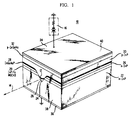
- the semiconductor light emitting device in FIG. 1 may be used as a laser or as an edge-emitting LED.
- the device 10 includes an active region 12 in which the recombination of electrons and holes causes radiation to be emitted at a wavelength characteristic of the bandgap of the semiconductor material of the active region (e.g., about 1.0-1.65 ⁇ m for InGaAsP depending on the specific composition of the alloy).
- the radiation is direction generally along axis 14 and is primarily stimulated emission in the case of a laser and primarily spontaneous emission in the case of an LED.
- This recombination radiation is generated by forward-biasing a p-n junction which causes minority carriers to be injected into the active region.
- Source 16 illustratively depicted as a battery in series with a current-limiting resistor, supplies the forward bias voltage and, in addition, provides pumping current at a level commensurate with the desired optical output power. In a laser, the pumping current exceeds the lasing current threshold.
- the device includes means for constraining the pumping current to flow in a relatively narrow channel through the active region 12.
- this constraining means comprises a bifurcated, high resistivity Fe-doped InP epitaxial layer 20, and the active region 12 has the shape of a stripe which lies in the rectangular opening (top view) of the bifurcated layer 20.
- the layer 20, rather than being bifurcated might take the shape of an annulus surround a cylindrical or mesa-like active region.
- FIG. 1 The structure shown in FIG. 1 is known as a channeled-substrate buried heterostructure (CSBH) laser which includes an n-InP substrate 22 and an Fe-doped high resistivity InP epitaxial layer 20 which is bifurcated by a groove 24.
- the groove is etched or otherwise formed through layer 20 into substrate 22.
- a preferred technique for controllably etching the groove in the shape of a V is described in U.S. Patent No. 4,595,454.
- n-InP first cladding layer 26 (the central portion of which fills at least the bottom portion of groove 24); an unintentionally doped InGaAsP layer 28; a p-InP second cladding layer 30; and a p-InGaAs (or p-InGaAsP) contact-facilitating layer 32.
- Layer 28 includes crescent-shaped active region 12 which, in practice, becomes separated from the remainder of layer 28 because epitaxial growth does not take place along the top edges of the groove 24.
- the active layer is preferably vertically positioned within the thickness of the high resistivity layer 20 in order to reduce leakage current.
- the active layer is below layer 20, but near enough thereto (i.e., ⁇ 1 ⁇ m away), leakage currents are still significantly reduced and nonradiative recombination at the layer 20 interface becomes much less of a problem.
- the high resistivity InP:Fe layer 20 is formed directly on the substrate 22, it may also be formed on an epitaxial buffer layer (not shown) grown on the substrate.
- an epitaxial buffer layer (not shown) grown on the substrate.
- a resistivity in excess of about 1 x 10⁶ ⁇ -cm is desirable.
- this aspect of the invention utilizes the growth of high resistivity InP:Fe layer 20 usisng hydride VPE with N2 as an inert carrier under conditions of limited PH3 pyrolysis in the reactor.
- the invention achieved transport of sufficient FeCl2 (and hence limited the excessive precipitation of iron by hydrogen) to produce InP:Fe with a resistivity of > 108 ⁇ -cm.
- a high resistivity layer prepared by this hydride VPE process maintains its high resistivity even after being subjected to the high temperatures of subsequent process (e.g., LPE) steps.
- Source 16 is connected across electrodes 34 and 36.
- FIG. 1 Although a broad-area cosdntact is depicted in FIG. 1 by layer 32 and electrode 34, it also is possible to delineate a stripe geometry contact as shown in FIG. 2.
- the contact-facilitating layer 32 ⁇ is etched to form a stripe and is aligned within the stripe-shaped opening of SiO2 layer 33.
- a stripe-shaped metal contact 35 is formed on layer 32 ⁇ in the opening of SiO2 layer 33, and a broad area electrode 34 ⁇ is then formed over the top of the device.
- a contact configuration of this type reduces device capacitance and hence increases high speed performance.
- the CSBH laser also includes means for providing optical feedback of the stimulated emission, typically a pair of separated, parallel, cleaved facets 38 and 40 which form an optical cavity resonator as shown in FIG. 1.
- the optical axis of the resonator and the elongated direction of the stripe-shaped active region 12 are generally parallel to one another.
- Other feedback techniques are also suitable, however, including well-known distributed feedback gratings, for example.
- This example describes the fabrication of high resistivity InP:Fe epitaxial layers by a hydride VPE process. These high resistivity layers can be incorporated into CSBH lasers (as described above) as well as into other device structures as described hereinafter.
- CSBH lasers as described above
- Other device structures as described hereinafter.
- the various materials, dimensions, concentrations, etc., are given by way of illustration only and are not intended to limit the invention unless otherwise stated.
- the reactor used for the growth of the InP:Fe is described by R. F. Karlicek et al. in Journal of Applied Physics , Vol. 60, p. 794 (1986).
- the source gases included HCl and PH3 mixtures (5% and 2%, respectively) in ultra high purity N2), and the N2 carrier gas (99.999% pure) was obtained from a standard compressed gas cylinder.
- the concentration of the input was reactive gases was selected using electronic mass flow controllers.
- the transport of iron as the dichloride FeCl2 was accomplished by flowing HCl (5% in N2) through iron powder (99.999% pure) placed on a quartz frit which was located downstream of the In (l) source in the reactor source region.
- the In (l) source temperature, the Fe source temperature, and the growth temperature were kept constant at about 700°C. Between growth experiments, Pd-purified H2 was made to flow through the reactor in place of N2.
- the extent of PH3 pyrolysis was determined by measuring the absorbance of P4 at 230 nm. Since P4 is the dominant species (except for unpyrolyzed PH3) the concentration of P2 was not monitored optically and was not included in the computation of the degree of PH3 pyrolysis during growth. The transport of FeCl2 was also monitored optically, and the concentration was computed from published thermodynamic data for the Fe-Cl system.
- the invention achieves sufficient transport of FeCl2 (and hence limited the escessive precipitation of iron by hydrogen) to produce InP:Fe with a resistivity of > 108 ⁇ -cm.
- InP:Fe The growth of InP:Fe was performed on ⁇ 100> oriented InP:S substrates which were degreased prior to placement in the reactor. Following the preheating of the substrate under a dilute PH3 flow, a brief etch was performed by initiating the flow of HCl through the Fe source. Growth was initiated by starting the flow of HCl over the In (l) source region.
- the specific growth conditions were as follows: PH3 pressure of 1755 Pa (17.9 x 10 ⁇ 3 atm), InCl pressure of 390 Pa (4.0 x 10 ⁇ 3 atm), HCl pressure of 9.8 Pa (0.1 x 10 ⁇ 3 atm), and total flow of 2250 sccm.
- the combination of the inert carrier gas (e.g., N2), the volatile dopant compound (e.g., FeCl2), the volatile indium compound (e.g., InCl) and the Group V hydride (e.g., PH3) are known as a precursor gas. These conditions produced in InP:Fe growth rates of 16 ⁇ m/hr. The resulting InP:Fe layer was measured to have a resistivity of about 2.4 x 10⁸ ⁇ -cm.
- the invention contemplates the ability to grow by hydride VPE InP-based epitaxial layers having the physical characteristics (e.g., resistivities of ⁇ 106 ⁇ -cm and thicknesses of ⁇ 1 ⁇ m) of Fe-doped InP-based layers grown by MOCVD.
- These InP-based layers include, for example, InGaP, InAsP, InGaAsP and InGaAlP.
- DCPBH double channel planar buried heterostructure
- the conventional DCPBH laser is described generally by I. Mito et al. in Journal of Lightwave Technology , Vol. LT-1, No. 1, p. 195 (1983). It employs LPE regrowth in the channels to form reverse-biased blocking junctions which constrain current to flow through the elongated mesa containing the active layer.
- LPE regrowth of blocking junctions is replaced by growth of InP:Fe zones 40 on each side of the mesa.
- a restricted (e.g., stripe geometry) contact 42 is delineated on top of the mesa by a patterned dielectric layer 44 (e.g., SiO2) and an electrode 46 overlays the top of the device.
- a patterned dielectric layer 44 e.g., SiO2
- an electrode 46 overlays the top of the device.
- the active region of the devices described above may include a single active layer or a composite several layers at least one of which is active (in the light-emitting sense).
- several active layers emitting at different wavelengths are also embraced within the definition of an active region.
Description
- This invention relates to a vapor phase epitaxial growth technique utilized to fabricate semiconductor devices such as light emitting devices, light detecting devices, and field-effect transistors.
- A common problem in the fabrication of low threshold buried heterostructure (BH) lasers in the InGaAsP/InP materials system is the control of leakage currents (i.e., currents which bypass the active region of the device). These currents lead to high lasing threshold, low differential quantum efficiency, abnormal temperature dependence of threshold current, and rollover of the light-current (L-I) characteristic. All of these factors have a significant negative impact on the use of BH lasers in transmitters for fiber optic communication systems.
- One possible solution to the problem of leakage current in buried heterostructure lasers is the controlled introduction of high resistivity material into the device structure. This high resistivity material could be used to block current flow through undesired leakage paths. Previously, high resistivity liquid phase epitaxial (LPE) Al0.65Ga0.35As (lightly Ge-doped) material has been utilized for current confinement in AlGaAs/GaAs buried heterostructure lasers, but subsequent attempts to produce high resistivity LPE InP material for this purpose have not been successful. Deuteron bombardment has also been shown to produce highly resistive material during subsequent processing. In particular, because the high resistivity is related to deuteron implant damage, the resistivity anneals out at the high temperatures (e.g., above about 600°C) required for subsequent LPE growth.
- In addition, bifurcated, reverse-biased p-n junctions have also been reported for constraining current to flow through the active region of InGaAsP/InP lasers. These blocking junctions have been fabricated by the implanation of Be into n-InP substrates, by the diffusion of Cd into n-InP substrates, and by the epitaxial growth of a p-InP layer onto an n-InP substrate. But, all of these devices are impaired to some extent by leakage currents because of the imperfect blocking characteristics of the reverse-biased junctions.
- More recently, D. P. Wilt et al. reported in Applied Physics Letters, Vol. 44, No. 3, p. 290 (Feb. 1984) that InP/InGaAsP CSBH lasers with relatively low leakage currents and low lasing thresholds cans be fabricated by incorporating into the structure a high resistivity Fe-ion-implanted layer which constrains pumping current to flow through the active region. The high resistivity layer is produced by an Fe-ion implant into an n-type InP substrate followed by an annealing treatment prior to LPE growth. Although the resistivity of the Fe-ion-implanted layer is stable even after being subjected to the high temperatures characteristic of LPE growth, the thinness of the Fe-implanted layer (about 0.4 µm) renders it difficult to reproducibly position the thin active layer (about 0.1-0.2 µm thick) adjacent thereto. When the active layer is not so placed, shunt paths are created which allow leakage current to flow around the active layer. Hence, high performance (low threshold, high efficiency) devices are hard to fabricate reproducibly.
- Others in the prior art have attempted to utilize hydride vapor phase epitaxy (VPE) to grow high resistivity Fe-doped InP, but his approach has been a difficult task because suitable volatile iron compounds typically cannot be transported using a hydrogen carrier gas at temperatures normally used for growth (e.g., T≧650°C). The growth of InP in an inert carrier gas is difficult as well and has been reported only for trichloride system (using PCl₃) when PH₃ was added to stimulate growth. See P. L. Giles et al., Journal of Crystal Growth, Vol. 61, p. 695 (1983).
- In accordance with one aspect of our invention, a method of fabricating a device, which includes an iron-doped, indium-based, compound Group III-V semiconductor region, comprises the steps of (1) forming a precursor gas comprising a carrier gas, a volatile dopant compound, a volatile indium compound and a Group V hydride, (2) directing the precursor gas through a heated chamber to contact a heated deposition body, and (3) inducing deposition of the compound semiconductor on the body, characterized in that the carrier gas comprises an inert gas, the volatile dopant compound includes iron and is formed by reaction of HCl with solid iron and the volatile indium compound is formed by reaction of HCl with liquid indium, wherein the presence of hydrogen in said precursor gas is limited to that formed by reacting HCl with the iron and indium and to the pyrolysis of the Group V hydride in the heated chamber, such that excessive precipitation of iron is prevented, and the concentrations of said volatile indium compound at the body and of the hydride are maintained sufficient to result in deposition of the semiconductor.
- In one embodiment, a semi-insulating, iron-doped, InP-based, compound Group III-V semiconductor region is fabricated by using a precursor gas comprising a nitrogen carrier, FeCl₂, InCl and PH₃, and the concentration of hydrogen in the precursor gas is limited by limiting the amount of pyrolysis of PH₃. This process is capable of producing a region having a resistivity greater than 10⁸ Ω-cm which is suitable for use as a current-blocking region in a number of devices; e.g., light emitting devices, light detecting devices and FETs.
- The invention, together with its various features and advantages, can be readily understood from the following, more detailed description taken in conjunction with the accompanying drawing, in which, in the interests of clarity, the figures have not been drawn to scale:
- FIG. 1 is an isometric view of a CSBH light emitting device fabricated in accordance with one embodiment of the invention;
- FIG. 2 is an end view of another CSBH device fabricated in accordance with another embodiment of the invention; and
- FIG. 3 is an end view of a DC-PBH device fabricated in accordance with still another embodiment of the invention.
- The semiconductor light emitting device in FIG. 1 may be used as a laser or as an edge-emitting LED. In either case, the
device 10 includes anactive region 12 in which the recombination of electrons and holes causes radiation to be emitted at a wavelength characteristic of the bandgap of the semiconductor material of the active region (e.g., about 1.0-1.65 µm for InGaAsP depending on the specific composition of the alloy). The radiation is direction generally alongaxis 14 and is primarily stimulated emission in the case of a laser and primarily spontaneous emission in the case of an LED. - This recombination radiation is generated by forward-biasing a p-n junction which causes minority carriers to be injected into the active region.
Source 16, illustratively depicted as a battery in series with a current-limiting resistor, supplies the forward bias voltage and, in addition, provides pumping current at a level commensurate with the desired optical output power. In a laser, the pumping current exceeds the lasing current threshold. - In general, the device includes means for constraining the pumping current to flow in a relatively narrow channel through the
active region 12. As illustrated, this constraining means comprises a bifurcated, high resistivity Fe-doped InPepitaxial layer 20, and theactive region 12 has the shape of a stripe which lies in the rectangular opening (top view) of the bifurcatedlayer 20. Note, in the case of a surface emitting LED thelayer 20, rather than being bifurcated, might take the shape of an annulus surround a cylindrical or mesa-like active region. - The structure shown in FIG. 1 is known as a channeled-substrate buried heterostructure (CSBH) laser which includes an n-
InP substrate 22 and an Fe-doped high resistivity InPepitaxial layer 20 which is bifurcated by agroove 24. The groove is etched or otherwise formed throughlayer 20 intosubstrate 22. A preferred technique for controllably etching the groove in the shape of a V is described in U.S. Patent No. 4,595,454. - The following essentially lattice-matched epitaxial layers are then epitaxially grown on the etched wafer: an n-InP first cladding layer 26 (the central portion of which fills at least the bottom portion of groove 24); an unintentionally doped
InGaAsP layer 28; a p-InPsecond cladding layer 30; and a p-InGaAs (or p-InGaAsP) contact-facilitatinglayer 32.Layer 28 includes crescent-shapedactive region 12 which, in practice, becomes separated from the remainder oflayer 28 because epitaxial growth does not take place along the top edges of thegroove 24. Provided that nonradiative recombination at the interface withhigh resistivity layer 20 is not significant, the active layer is preferably vertically positioned within the thickness of thehigh resistivity layer 20 in order to reduce leakage current. However, if the active layer is belowlayer 20, but near enough thereto (i.e., ≦ 1 µm away), leakage currents are still significantly reduced and nonradiative recombination at thelayer 20 interface becomes much less of a problem. - Although the high resistivity InP:
Fe layer 20 is formed directly on thesubstrate 22, it may also be formed on an epitaxial buffer layer (not shown) grown on the substrate. For CSBH InP/InGaAsP lasers a resistivity in excess of about 1 x 10⁶ Ω-cm is desirable. In either case, this aspect of the invention utilizes the growth of high resistivity InP:Fe layer 20 usisng hydride VPE with N₂ as an inert carrier under conditions of limited PH₃ pyrolysis in the reactor. By using an inert carrier and limiting the presence of H₂ to that formed by the reaction of HCl with In(l) and Fe(s) and the pyrolysis of PH₃, the invention achieved transport of sufficient FeCl₂ (and hence limited the excessive precipitation of iron by hydrogen) to produce InP:Fe with a resistivity of > 10⁸ Ω-cm. - A high resistivity layer prepared by this hydride VPE process maintains its high resistivity even after being subjected to the high temperatures of subsequent process (e.g., LPE) steps.
- Electrical contact is made to the device via
metal electrodes layer 32 andsubstrate 22, respectively.Source 16 is connected acrosselectrodes - Although a broad-area cosdntact is depicted in FIG. 1 by
layer 32 andelectrode 34, it also is possible to delineate a stripe geometry contact as shown in FIG. 2. Here components with primed notation in FIG. 2 correspond to those with the same reference numerals in FIG. 1. Thus, the contact-facilitating layer 32ʹ is etched to form a stripe and is aligned within the stripe-shaped opening ofSiO₂ layer 33. A stripe-shaped metal contact 35 is formed on layer 32ʹ in the opening ofSiO₂ layer 33, and a broad area electrode 34ʹ is then formed over the top of the device. A contact configuration of this type reduces device capacitance and hence increases high speed performance. - The CSBH laser also includes means for providing optical feedback of the stimulated emission, typically a pair of separated, parallel,
cleaved facets active region 12 are generally parallel to one another. Other feedback techniques are also suitable, however, including well-known distributed feedback gratings, for example. - This example describes the fabrication of high resistivity InP:Fe epitaxial layers by a hydride VPE process. These high resistivity layers can be incorporated into CSBH lasers (as described above) as well as into other device structures as described hereinafter. The various materials, dimensions, concentrations, etc., are given by way of illustration only and are not intended to limit the invention unless otherwise stated.
- The reactor used for the growth of the InP:Fe is described by R. F. Karlicek et al. in Journal of Applied Physics, Vol. 60, p. 794 (1986). The source gases included HCl and PH₃ mixtures (5% and 2%, respectively) in ultra high purity N₂), and the N₂ carrier gas (99.999% pure) was obtained from a standard compressed gas cylinder. The concentration of the input was reactive gases was selected using electronic mass flow controllers. The transport of iron as the dichloride FeCl₂ was accomplished by flowing HCl (5% in N₂) through iron powder (99.999% pure) placed on a quartz frit which was located downstream of the In(l) source in the reactor source region. The In(l) source temperature, the Fe source temperature, and the growth temperature were kept constant at about 700°C. Between growth experiments, Pd-purified H₂ was made to flow through the reactor in place of N₂.
- Using an optical spectrometer which monitored the wavelength region between 200 and 330 nm, the extent of PH₃ pyrolysis was determined by measuring the absorbance of P₄ at 230 nm. Since P₄ is the dominant species (except for unpyrolyzed PH₃) the concentration of P₂ was not monitored optically and was not included in the computation of the degree of PH₃ pyrolysis during growth. The transport of FeCl₂ was also monitored optically, and the concentration was computed from published thermodynamic data for the Fe-Cl system.
- As noted earlier, by using an inert carrier gas and limiting the presence of hydrogen to that formed by the reaction of HCl with liquid indium and solid iron and by the pyrolysis of phosphine, the invention achieves sufficient transport of FeCl₂ (and hence limited the escessive precipitation of iron by hydrogen) to produce InP:Fe with a resistivity of > 10⁸ Ω-cm.
- The growth of InP:Fe was performed on <100> oriented InP:S substrates which were degreased prior to placement in the reactor. Following the preheating of the substrate under a dilute PH₃ flow, a brief etch was performed by initiating the flow of HCl through the Fe source. Growth was initiated by starting the flow of HCl over the In(l) source region. The specific growth conditions were as follows: PH₃ pressure of 1755 Pa (17.9 x 10⁻³ atm), InCl pressure of 390 Pa (4.0 x 10⁻³ atm), HCl pressure of 9.8 Pa (0.1 x 10⁻³ atm), and total flow of 2250 sccm. The combination of the inert carrier gas (e.g., N₂), the volatile dopant compound (e.g., FeCl₂), the volatile indium compound (e.g., InCl) and the Group V hydride (e.g., PH₃) are known as a precursor gas. These conditions produced in InP:Fe growth rates of 16 µm/hr. The resulting InP:Fe layer was measured to have a resistivity of about 2.4 x 10⁸ Ω-cm.
- In addition, the invention contemplates the ability to grow by hydride VPE InP-based epitaxial layers having the physical characteristics (e.g., resistivities of ≧ 10⁶ Ω-cm and thicknesses of ≧ 1 µm) of Fe-doped InP-based layers grown by MOCVD. These InP-based layers include, for example, InGaP, InAsP, InGaAsP and InGaAlP.
- Moreover, while the invention has been discussed with reference to lasers and LEDs, it will be appreciated by those skilled in the art that it is applicable to other semiconductor devices (e.g., photodiodes, FETs) in which substantial current is prevented from flowing through a region of the device.
- One alternative laser structure which may be fabricated in accordance with the invention is known as the double channel planar buried heterostructure (DCPBH). The conventional DCPBH laser is described generally by I. Mito et al. in Journal of Lightwave Technology, Vol. LT-1, No. 1, p. 195 (1983). It employs LPE regrowth in the channels to form reverse-biased blocking junctions which constrain current to flow through the elongated mesa containing the active layer. In accordance with a DCPBH embodiment of the invention shown in FIG. 3, however, the LPE regrowth of blocking junctions is replaced by growth of InP:
Fe zones 40 on each side of the mesa. A restricted (e.g., stripe geometry)contact 42 is delineated on top of the mesa by a patterned dielectric layer 44 (e.g., SiO₂) and anelectrode 46 overlays the top of the device. In this fashion, current is constrained by the InP:Fe zones 40 and thedielectric layer 44 to flow essentially only through the mesa and hence through theactive layer 50. - Finally, it is well known that the active region of the devices described above may include a single active layer or a composite several layers at least one of which is active (in the light-emitting sense). Thus, in a 1.55 µm InP/InGaAsP laser, the active region may include an InGaAsP layer which emsits light at 1.55 µm adjacent another InGaAsP layer (λ=1.3 µm) which serves an anti-meltback function during LPE growth. Moreover, several active layers emitting at different wavelengths are also embraced within the definition of an active region.
Claims (10)
- A method of fabricating a device, which includes an iron-doped, indium-based, compound Group III-V semiconductor region, comprising the steps of (1) forming a precursor gas comprising a carrier gas, a volatile dopant compound, a volatile indium compound and a Group V hydride, (2) directing said precursor gas through a heated chamber to contact a heated deposition body, and (3) inducing deposition of said compound semiconductor on said body, characterized in that the carrier gas comprises an inert gas, the volatile dopant compound includes iron and is formed by reaction of HCl with solid iron and the volatile indium compound is formed by reaction of HCl with liquid indium, wherein the presence of hydrogen in said precursor gas is limited to that formed by reacting HCl with the iron and indium and to the pyrolysis of the Group V hydride in the heated chamber, such that excessive precipitation of iron is prevented, and the concentrations of said volatile indium compound at said body and of said Group V hydride are maintained sufficient to result in said deposition.
- The method of claim 1 wherein the presence of hydrogen is limited by limiting the amount of pyrolysis of said hydride.
- The method of claim 2 wherein said inert carrier gas comprises nitrogen.
- The method of claim 2 or claim 3 wherein said volatile indium compound comprises InCl.
- The method of any of claims 2 to 4 wherein said volatile dopant compound comprises FeCl₂.
- The method of any of claims 2 to 5 wherein said hydride comprises phosphine.
- The method of claim 6 wherein said region comprises high resistivity InP.
- The method of claim 7 wherein said region has a resistivity greater than 10⁸Ω-cm.
- The method of claim 2 wherein said region comprises high resistivity InP and said carrier gas comprises nitrogen, said volatile indium compound comprises InCl, said volatile dopant compound comprises FeCl₂, and said hydride comprises phosphine.
- The method of any of claims 1 to 9 wherein said body has a mesa thereon and said deposition forms said region adjacent said mesa.
Applications Claiming Priority (2)
| Application Number | Priority Date | Filing Date | Title |
|---|---|---|---|
| US491987A | 1987-01-20 | 1987-01-20 | |
| US4919 | 1987-01-20 |
Publications (3)
| Publication Number | Publication Date |
|---|---|
| EP0276069A2 EP0276069A2 (en) | 1988-07-27 |
| EP0276069A3 EP0276069A3 (en) | 1989-02-15 |
| EP0276069B1 true EP0276069B1 (en) | 1992-12-16 |
Family
ID=21713183
Family Applications (1)
| Application Number | Title | Priority Date | Filing Date |
|---|---|---|---|
| EP88300203A Expired - Lifetime EP0276069B1 (en) | 1987-01-20 | 1988-01-12 | Vapor phase epitaxial growth of iron-doped, indium-based, compound group iii-v semiconductors |
Country Status (6)
| Country | Link |
|---|---|
| EP (1) | EP0276069B1 (en) |
| JP (1) | JPS63193897A (en) |
| KR (1) | KR960015483B1 (en) |
| CA (1) | CA1282874C (en) |
| DE (1) | DE3876639T2 (en) |
| ES (1) | ES2036260T3 (en) |
Cited By (1)
| Publication number | Priority date | Publication date | Assignee | Title |
|---|---|---|---|---|
| EP1000291A1 (en) † | 1998-04-28 | 2000-05-17 | Advanced Technology Materials, Inc. | Fluid storage and dispensing system |
Families Citing this family (2)
| Publication number | Priority date | Publication date | Assignee | Title |
|---|---|---|---|---|
| US5608234A (en) * | 1994-11-14 | 1997-03-04 | The Whitaker Corporation | Semi-insulating edge emitting light emitting diode |
| EP0712169A1 (en) * | 1994-11-14 | 1996-05-15 | The Whitaker Corporation | Semi-insulating edge emitting light emitting diode |
Family Cites Families (5)
| Publication number | Priority date | Publication date | Assignee | Title |
|---|---|---|---|---|
| US4062706A (en) * | 1976-04-12 | 1977-12-13 | Robert Arthur Ruehrwein | Process for III-V compound epitaxial crystals utilizing inert carrier gas |
| JPS5379459A (en) * | 1976-12-24 | 1978-07-13 | Fujitsu Ltd | Doping prodess device |
| US4314873A (en) * | 1977-07-05 | 1982-02-09 | The United States Of America As Represented By The Secretary Of The Navy | Method for depositing heteroepitaxially InP on GaAs semi-insulating substrates |
| CA1210526A (en) * | 1983-10-21 | 1986-08-26 | Judith A. Long | Device having semi-insulating indium phosphides based compositions |
| JPS6218078A (en) * | 1985-07-17 | 1987-01-27 | Nec Corp | Buried structure semiconductor laser and manufacture of the same |
-
1988
- 1988-01-12 DE DE8888300203T patent/DE3876639T2/en not_active Expired - Lifetime
- 1988-01-12 ES ES198888300203T patent/ES2036260T3/en not_active Expired - Lifetime
- 1988-01-12 EP EP88300203A patent/EP0276069B1/en not_active Expired - Lifetime
- 1988-01-18 CA CA000556706A patent/CA1282874C/en not_active Expired - Lifetime
- 1988-01-18 KR KR1019880000327A patent/KR960015483B1/en not_active IP Right Cessation
- 1988-01-19 JP JP63007669A patent/JPS63193897A/en active Granted
Cited By (2)
| Publication number | Priority date | Publication date | Assignee | Title |
|---|---|---|---|---|
| EP1000291A1 (en) † | 1998-04-28 | 2000-05-17 | Advanced Technology Materials, Inc. | Fluid storage and dispensing system |
| EP1000291B2 (en) † | 1998-04-28 | 2009-06-24 | Advanced Technology Materials, Inc. | Fluid storage and dispensing system |
Also Published As
| Publication number | Publication date |
|---|---|
| DE3876639D1 (en) | 1993-01-28 |
| KR960015483B1 (en) | 1996-11-14 |
| EP0276069A3 (en) | 1989-02-15 |
| DE3876639T2 (en) | 1993-04-22 |
| EP0276069A2 (en) | 1988-07-27 |
| ES2036260T3 (en) | 1993-05-16 |
| JPS63193897A (en) | 1988-08-11 |
| CA1282874C (en) | 1991-04-09 |
| JPH0543680B2 (en) | 1993-07-02 |
| KR880009417A (en) | 1988-09-15 |
Similar Documents
| Publication | Publication Date | Title |
|---|---|---|
| US4888624A (en) | Semiconductor devices employing high resistivity in-based compound group III-IV epitaxial layer for current confinement | |
| EP0185051B1 (en) | Semiconductor devices with buried heterostructure | |
| CA1276276C (en) | Semiconductor devices employing ti-doped group iii-v epitaxial layer | |
| Nakamura et al. | CW operation of distributed‐feedback GaAs‐GaAlAs diode lasers at temperatures up to 300 K | |
| JP2823476B2 (en) | Semiconductor laser and method of manufacturing the same | |
| EP0201599B1 (en) | The fabrication of grooved semiconductor devices | |
| EP0038085B1 (en) | Buried heterostructure laser diode and method for making the same | |
| US4999315A (en) | Method of controlling dopant incorporation in high resistivity In-based compound Group III-V epitaxial layers | |
| KR100187778B1 (en) | Buried heterostructure lasers using mocvd growth over patterned substrates | |
| US5260230A (en) | Method of manufacturing buried heterostructure semiconductor laser | |
| EP0462816B1 (en) | Semiconductor laser producing visible light | |
| EP0473443B1 (en) | Buried-stripe type semiconductor laser device | |
| EP0276069B1 (en) | Vapor phase epitaxial growth of iron-doped, indium-based, compound group iii-v semiconductors | |
| JP4002422B2 (en) | Semiconductor device and manufacturing method thereof | |
| JPH11506273A (en) | Radiation-emitting semiconductor diode with a separate confinement layer of a semiconductor material containing up to 30% of aluminum or a semiconductor material without aluminum | |
| US4517674A (en) | Zinc-diffused narrow stripe AlGaAs/GaAs double heterostructure laser | |
| Yoshikawa et al. | A novel technology for formation of a narrow active layer in buried heterostructure lasers by single-step MOCVD | |
| Mawatari et al. | Reliability and degradation behaviors of semi-insulating Fe-doped InP buried heterostructure lasers fabricated by RIE and MOVPE | |
| Inoue et al. | Fabrication of AlxGa1-xAs buried heterostructure laser diodes by in-situ gas etching and selective-area metalorganic vapor phase epitaxy | |
| Yang et al. | High‐power broad‐area lasers fabricated by selective area growth | |
| Hafich et al. | AlGaAs/GaAs transverse junction stripe lasers with distributed feedback | |
| Takahashi et al. | Low threshold current coplanar vertical injection laser diode for optoelectronic integrated circuits | |
| JPH03256388A (en) | Manufacture of semiconductor laser | |
| JPH0770784B2 (en) | Lateral injection laser and manufacturing method thereof |
Legal Events
| Date | Code | Title | Description |
|---|---|---|---|
| PUAI | Public reference made under article 153(3) epc to a published international application that has entered the european phase |
Free format text: ORIGINAL CODE: 0009012 |
|
| AK | Designated contracting states |
Kind code of ref document: A2 Designated state(s): DE ES FR GB IT NL SE |
|
| PUAL | Search report despatched |
Free format text: ORIGINAL CODE: 0009013 |
|
| AK | Designated contracting states |
Kind code of ref document: A3 Designated state(s): DE ES FR GB IT NL SE |
|
| 17P | Request for examination filed |
Effective date: 19890809 |
|
| 17Q | First examination report despatched |
Effective date: 19910208 |
|
| GRAA | (expected) grant |
Free format text: ORIGINAL CODE: 0009210 |
|
| AK | Designated contracting states |
Kind code of ref document: B1 Designated state(s): DE ES FR GB IT NL SE |
|
| REF | Corresponds to: |
Ref document number: 3876639 Country of ref document: DE Date of ref document: 19930128 |
|
| ET | Fr: translation filed | ||
| ITF | It: translation for a ep patent filed |
Owner name: MODIANO & ASSOCIATI S.R.L. |
|
| REG | Reference to a national code |
Ref country code: ES Ref legal event code: FG2A Ref document number: 2036260 Country of ref document: ES Kind code of ref document: T3 |
|
| PLBE | No opposition filed within time limit |
Free format text: ORIGINAL CODE: 0009261 |
|
| STAA | Information on the status of an ep patent application or granted ep patent |
Free format text: STATUS: NO OPPOSITION FILED WITHIN TIME LIMIT |
|
| 26N | No opposition filed | ||
| EAL | Se: european patent in force in sweden |
Ref document number: 88300203.2 |
|
| PGFP | Annual fee paid to national office [announced via postgrant information from national office to epo] |
Ref country code: SE Payment date: 20001227 Year of fee payment: 14 |
|
| PGFP | Annual fee paid to national office [announced via postgrant information from national office to epo] |
Ref country code: ES Payment date: 20010118 Year of fee payment: 14 |
|
| REG | Reference to a national code |
Ref country code: GB Ref legal event code: IF02 |
|
| PG25 | Lapsed in a contracting state [announced via postgrant information from national office to epo] |
Ref country code: SE Free format text: LAPSE BECAUSE OF NON-PAYMENT OF DUE FEES Effective date: 20020113 |
|
| PG25 | Lapsed in a contracting state [announced via postgrant information from national office to epo] |
Ref country code: ES Free format text: LAPSE BECAUSE OF NON-PAYMENT OF DUE FEES Effective date: 20020114 |
|
| EUG | Se: european patent has lapsed |
Ref document number: 88300203.2 |
|
| REG | Reference to a national code |
Ref country code: ES Ref legal event code: FD2A Effective date: 20030922 |
|
| PGFP | Annual fee paid to national office [announced via postgrant information from national office to epo] |
Ref country code: NL Payment date: 20070109 Year of fee payment: 20 |
|
| PGFP | Annual fee paid to national office [announced via postgrant information from national office to epo] |
Ref country code: DE Payment date: 20070110 Year of fee payment: 20 |
|
| PGFP | Annual fee paid to national office [announced via postgrant information from national office to epo] |
Ref country code: GB Payment date: 20070119 Year of fee payment: 20 |
|
| PGFP | Annual fee paid to national office [announced via postgrant information from national office to epo] |
Ref country code: IT Payment date: 20070626 Year of fee payment: 20 |
|
| REG | Reference to a national code |
Ref country code: GB Ref legal event code: PE20 |
|
| NLV7 | Nl: ceased due to reaching the maximum lifetime of a patent |
Effective date: 20080112 |
|
| PG25 | Lapsed in a contracting state [announced via postgrant information from national office to epo] |
Ref country code: NL Free format text: LAPSE BECAUSE OF EXPIRATION OF PROTECTION Effective date: 20080112 |
|
| PGFP | Annual fee paid to national office [announced via postgrant information from national office to epo] |
Ref country code: FR Payment date: 20070111 Year of fee payment: 20 |
|
| PG25 | Lapsed in a contracting state [announced via postgrant information from national office to epo] |
Ref country code: GB Free format text: LAPSE BECAUSE OF EXPIRATION OF PROTECTION Effective date: 20080111 |