EP0273136A2 - Universelles Peripheriesteuerungsmodul mit Konfigurationsladung während der Initialisierung - Google Patents
Universelles Peripheriesteuerungsmodul mit Konfigurationsladung während der Initialisierung Download PDFInfo
- Publication number
- EP0273136A2 EP0273136A2 EP87115987A EP87115987A EP0273136A2 EP 0273136 A2 EP0273136 A2 EP 0273136A2 EP 87115987 A EP87115987 A EP 87115987A EP 87115987 A EP87115987 A EP 87115987A EP 0273136 A2 EP0273136 A2 EP 0273136A2
- Authority
- EP
- European Patent Office
- Prior art keywords
- bus
- upc
- recited
- computer system
- peripheral devices
- Prior art date
- Legal status (The legal status is an assumption and is not a legal conclusion. Google has not performed a legal analysis and makes no representation as to the accuracy of the status listed.)
- Withdrawn
Links
Images


Classifications
-
- G—PHYSICS
- G06—COMPUTING OR CALCULATING; COUNTING
- G06F—ELECTRIC DIGITAL DATA PROCESSING
- G06F15/00—Digital computers in general; Data processing equipment in general
- G06F15/16—Combinations of two or more digital computers each having at least an arithmetic unit, a program unit and a register, e.g. for a simultaneous processing of several programs
- G06F15/177—Initialisation or configuration control
-
- G—PHYSICS
- G06—COMPUTING OR CALCULATING; COUNTING
- G06F—ELECTRIC DIGITAL DATA PROCESSING
- G06F13/00—Interconnection of, or transfer of information or other signals between, memories, input/output devices or central processing units
- G06F13/38—Information transfer, e.g. on bus
- G06F13/382—Information transfer, e.g. on bus using universal interface adapter
- G06F13/385—Information transfer, e.g. on bus using universal interface adapter for adaptation of a particular data processing system to different peripheral devices
Definitions
- This invention relates generally to data processing systems having data processing operations provided over a common input/output bus, and more particularly with a universal peripheral controller for controlling various types and numbers of peripherals coupled to the bus.
- Many data processing systems include a common bus to which a plurality of units are connected for the transfer of information.
- the bus permits any two units to communicate with each other at a given time via a common (shared) signal path.
- Any unit wishing to communicate requests the bus cycle. When that bus cycle is granted, that unit becomes the master and may address any other unit in the system as the slave. Most transfers are in the direction of a master to a slave.
- Some types of bus interchange require a response cycle (read memory, for example). In cases where a response cycle is required, the requester assumes the role of the master, indicates a response is required, and identifies itself to the slave.
- the slave When the required information becomes available (depending on slave response time), the slave now assumes the role of the master and initiates a transfer to the requesting unit. This completes the interchange which has taken two bus cycles. Intervening time on the bus between these two cycles may be used for other system traffic not involving these two units.
- a master may address any other unit on the bus as a slave. It does this by placing the slave address on the address leads.
- the bus enables up to 224 bytes to be directly addressed to memory.
- units are passing control information, data or interrupts, they address each other by a channel number.
- the channel number allows up to 210 channels to be addressed by the bus.
- a 6 bit function code is passed which specifies which up to 26 possible functions this transfer implies.
- a typical prior art data processing system utilizing a bus is shown in Figure 1.
- a multiline bus 100 coupled with memory 102 to memory 104, such memories having the highest priority and with the central processor 106 having the lowest priority.
- Also connected on the bus may be included, for example, a scientific-arithmetic unit 108 and various controllers 110, 112, 114.
- Controller 110 may be coupled to control, for example, 4 unit record peripheral devices 116.
- Controller 112 may be used to provide communication control via modem devices; whereas controller 114 may be utilized to control mass storage devices, such as a tape peripheral device 118 or a disk peripheral device 120.
- Any one of the devices coupled with the bus 100 may address a memory or any other unit connected to the bus.
- tape peripheral 118 may, via controller 114, address memory 102.
- Each of such units directly connected to the bus includes tie-breaking logic in the event that two units request simultaneous service from the bus further.
- a channel number exists for every end point in the particular system with the exception of the memory type processing elements which are identified by the memory address.
- a channel number is assigned for each such device.
- Full duplex devices, as well as half duplex devices, utilize two channel numbers.
- Output only or input only devices use only one channel number each.
- Channel numbers are easily variable and accordingly one or more hexidecimal rotary switches (thumb wheel switches) may be utilized for each such unit connected with the bus to indicate a set's unit address.
- the channel number may be designated for the particular unit connected to the bus, as may be appropriate for that particular system. Units with multiple inputs/outputs generally will require a block of consecutive channel numbers.
- a 4 port unit may use rotary switches to assign the upper 7 bits of a channel number and may use the lower order 3 bits thereof to define the port number to distinguish input ports from output ports.
- the channel number of the slave unit will appear on the address bus for all non-memory transfers. Each unit compares that number with its own internally stored number (internally stored by means of the rotary switches). The unit which achieves a compare is, by definition, the slave, and must respond to that cycle. Generally, no two points in a single system will be assigned to the same channel number.
- the function codes may designate output or input operations. All odd function codes designate output transfers (write), while all even function codes designate input transfer requests (read).
- the central processor examines the least significant bit of a 6 bit function code field for an input/output command and uses a bus lead to designate the direction.
- a unique device identification number is assigned to every different type of device which is connected to the bus. This number is presented on the bus in response to the input function command, entitled input device identification.
- a unit wishing to interrupt the central processor requests the bus cycle. When this bus cycle is granted, the unit places its interrupt vector on the bus, the interrupt vector including the channel number of the central processor and the interrupt level number. The unit thus provides, as its interrupt vector, the master's channel number and its interrupt level number. If this is the central processor's channel number, the central processor will accept the interrupt if the level presented is numerically smaller than the current internal central processor level and if the central processor has not just accepted another interrupt.
- the memory has the highest priority and the central processor has the lowest priority, and they reside physically at opposite ends of the bus 100.
- Other units occupy intermediate positions and have priority which increases relative to their proximity to the memory end of the bus.
- a universal peripheral controller may be called to service different systems.
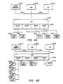
- Figure 4 there is shown, for simplicity only, two systems Figure 4A and Figure 4B, each with a different peripheral configuration of the invention.
- System A having a system controller 401A, RAM 402A and central subsystem (CSS) 403A, a bus 404A and 405A, may have several adapters 406A-0, 1, 2, 3 attached to it which the UPC must service.
- Adapter 0 may have two 1/2" tape drives 408A, 409A; adapter 406A-1 may have a printer 411A; adapter 2 may have an IEEE 488 interface device 412A; and adapter 3 may have one diskette drive 413A.
- System B also having a system controller 401B, Ram 402B and central subsystem (CSS) 403B, a bus 404B and 405B, may also have adapters 407B-0, 1, 2, 3 attached, but the configuration may be different as follows: adapter 407B-0 may have 4 1/2" tape drives 400B, 408B, 409B, 410B; adapter 1 may have a 1/4" tape streamer 413B; adapter 2 may have a diskette drive 411B-1; whereas adapter 3 may have a printer 417B.
- UPC universal peripheral controller
- Ramware (a trademark of Honeywell Information Systems Inc.) that could change the PROM to conform to the configuration of peripheral adapters actually attached.
- Another major object of the invention is to provide an improved data processing system having an improved bus architecture.
- Still another object of the invention is to provide a universal peripheral controller that could be compatible with different computer peripheral configurations.
- Yet another object of the invention is to provide a universal peripheral controller that could accommodate the coupling of different types of peripheral devices to the Megabus.
- Yet a further object of the invention is to provide a universal peripheral controller that would permit several levels of simultaneity in the transfer of data on the bus.
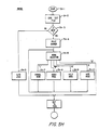
- the Universal Peripheral Controller Subsystem provides a common controller, the universal peripheral controller (UPC) 209 for all Megabus 204, 205 input/output (I/O) configurations with a facility to interface with a variety of peripheral devices.
- UPC universal peripheral controller
- the UPC permits four simultaneous data transfers as well as peripheral control functions on channels that are not busy.
- the UPC supports a high priority, low data rate section of the Megabus 204 or a low priority, high data rate section of the Megabus 205.
- the Megabus can further support either a 16 or 32 bit data bus and either a 24 or 32 address bus.
- Shown on Figure 2 coupled to the Megabus 204, 205 are typically a controller 201 which may be in part the system management hardware (SMF) 200 for which an application assigned to the same assignee as the instant application has been filed (see Related Applications), a Megabus memory 202 and a central subsystem (CSS) 203.
- SMF system management hardware
- CCS central subsystem
- the universal peripheral controller 209 can couple to either the high priority, low data rate section of Megabus 204 via a data bus 207a, which may be either 16 or 32 bits wide and an address bus 207b, which may be either 24 or 32 bits wide to provide an interface assembly enabling any Megabus I/O configuration to communicate with UPC/adapter connected peripherals.
- the UPCS further includes up to 4 peripheral adapters 212, each adapter having 2 or more logical channels, for a total of up to 8 logical channels although more channels may be handled by an adapter. Coupled to the adapters via UPC controller 209 are typical peripherals, such as tape peripheral 213, disk peripheral 214 and unit record peripherals 215a, 215b.
- adapters provide some data buffering; i.e., registers, for data rate synchronization and for error detection.
- a test connector 210 which may also be an integral part of the UPC and further includes RAM A 250.
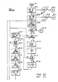
- a commercially available Motorola 68000 type microprocessor ( ⁇ P) 301 is coupled to internal data and address buses 325, 326 respectively.
- the data bus may be either 16 and 2 parity bits wide; whereas the address bus may be either 24 bits wide.
- a commercially available PROM 302 is also coupled to the data and address buses 325, 326 and is also coupled to commercially available control decoders 314.
- a commercially available dynamic random access memory (DRAM) 303 is further coupled to the data and address bus lines 325, 326 and is further coupled to the MY COMMAND register 315.
- DRAM dynamic random access memory
- the DRAM 303 may have storage capacity for at least 64K words and is provided with random logic implementation to refresh information stored therein.
- a bus timer 304 is coupled to the data address bus 325 and provides three functions. The first function is to detect if there is no response to a request for the bus and notify the ⁇ P. The second function of the bus timer 304 is to determine if the instruction being executed takes longer than a predetermined value and whether or not it has to abort the execution of the instruction. Finally, the third function of the bus timer 304 is to determine if there is a direct memory access (DMA) request cycle which takes longer than a predetermined period and abort that DMA cycle.
- DMA direct memory access
- a global data and address bus 316 is coupled to data and address lines 325, 326, respectively, via a commercially available transceiver 313.
- the global data and address bus 316 is further coupled to the interface 324 of the Megabus.
- the global data and address bus 316 is coupled to ports 309, 311, 322 and 323, respectively, (see Sheet 2 of Fig. 3) via commercially available transceivers 310 through path 327.
- Each port 309, 311, 322 and 323, has a respective adapter coupled to it, 309a, 311a, 322a, and 323a.
- the global data and address bus 316 has MY address register 319 and MY data register 321 coupled to it. These registers 319, 321 each have 4 words each.
- MY data register 321 has words A, B, C, D, each 8 bits wide plus a parity bit. While MY address register 319 also has 4 words E, F, G, H, each 8 bits wide plus a parity bit. These words and data and address registers 321, 319, respectively, correspond to data and address registers A, B, C, D, and E, F, G, H, located in the Megabus interface 324. Also in the Megabus interface 324 are command registers 252 each having 8 bits including a parity bit, and are each individually and sequentially marked 0---7 P, 8---15 P, etc. Also included in the Megabus interface 324 are commercially available 26S10 type transceivers 253.
- the gist of the peripheral controller is to have the ⁇ P 301 set up the paths for a dialog from a peripheral device requesting service through transceivers 313, global bus 316, Megabus interface 324, transceivers 310, ports 309, 311, 322, 323, and finally through adapters 309a, 311a, 322a, 323a, and on to the specific peripheral devices and to further provide address and range information to the DMA chips 305, 306 via transceiver 313, global bus 316 and transceiver 312.
- devices 213, 214, 215 attached to the UPC, through adapters 212 are software addressable via channel numbers. Each individual device has two channel numbers assigned, differing from each other only in the low order bit value (the direction bit). Channel assignments on the Megabus are made utilizing Figure 5A. Bits 8-17 of the address bus are utilized to select the adapter channel. Bits 8-13 are utilized for the most significant (MS) portion of the channel number; whereas bits 14-16 are utilized for the least significant (LS) portion. Bit 17 is the direction bit wherein a read (input) operation is performed when it is set to 0, and a write (output) operation is performed when it is set to 1.
- Channel assignments are as follows: Channel n Channel n + 080 Channel n + 100 Channel n + 180 Channel n + 200 Channel n + 280 Channel n + 300 Channel n + 380
- the direction bit of the output address channel number specifies whether it is going to be an input or an output data transfer; for all other commands, the direction bit is ignored.
- Bits 8-17 are assigned at system installation. Software visibility of the devices attached to the UPC is such that the devices are independent of each other; except that initiation of a command sequence addressed to one device may be stalled while the UPC is busy servicing another device on the same port but on a different channel.
- each channel Associated with each channel is a set of registers which are loaded by software and specify parameters required for attached device operation.
- range and the address registers (Figs. 6A - 6D), used for DMA operation, there are configuration registers (Figs. 6E - 6F) which contain record location and identification information and a task register for command codes.
- To perform a specific operation software first loads the address, range and configuration registers. The task register is loaded last with a command to be performed which also triggers the UPC channel operation. Commands addressed to a not busy channel are always accepted, but execution may be delayed because another channel on the same port is in the process of data transfer.
- the procedure is invoked by the system management function (SMF) 200 on detection of Power On signal from the system power supply (not shown). After running self test diagnostics, the SMF loads the central subsystem (CSS) 203 operating firmware from a Ramware diskette or a system disk.
- SMF system management function
- the SMF loads and starts the bootstrap load of operating system which then invokes the Ramware load utility (discussed infra).
- the Ramware load utility routine scans I/O ID (input/output identification) numbers from #0000-#FFFF looking for controllers which require Ramware loading.
- the adapter Ramware is loaded next and the Ramware Load Status bits 13 (on all channels) and 14 (this channel) are set to ONE if the loading is successful; if not, at any IOLD step, bit 15 is set to ONE and the software utility, retries that failed IOLD one more time. If multiple channels on the UPC require the same Ramware load, these channels should have their Ramware Load Status bit 14 also set; this avoids loading multiple copies of the same Ramware.
- PROM 302 a base intelligence is maintained that interrogates the identification (ID) of the currently attached adapters and via Megabus request and response instructions (infra) and together with the SMF (system management facility) 200 seeks out from the bootload device the personality (Ramware) that corresponds with that specific adapter's ID.
- This Ramware will be loaded into the corresponding local DRAM 303 associated with the physical port of the adapter. If two or more ports have the same type adapter, the Ramware will be written into the corresponding RAM locations by cloning, thus reducing system configuration time.
- the Ramware load utility is as follows: Load the I/O ID list from the load medium into memory Load the revs list from the load medium into memory Scan the ID entries for those requiring loadable peripheral Ramware Match the ID with valid IDs found in the IDLIST Determine if motherboard or adapter board Ramware is to be loaded Get the board hardware revision Using the board name and the hardware revision, determine Ramware to be loaded using IOREVS Load Ramware file into memory Prepare board for load sequence Load Ramware from memory into RAM Validate the loading sequence Determine next load device or channel Continue until all necessary Ramware is loaded Exit to operation system
- the program starts at 5H-1.
- the text file is loaded. This text file contains all the messages that are used by the utility load program and they are separated in a separate module to facilitate foreign language translation by affiliates.
- the text file is stored on a load medium and is loaded into main memory 202 from the load medium.
- the load media may be a diskette not part of the UPC system, or it may be part of the UPC system, or still another load media such as a disk that is not part of the UPC load system.
- 5H-4, 6, 7, 8, 9 and 10 are some of the internal debug utilities that are used where more help can be printed, a manual load can be achieved, or other debug purposes and is not necessary for the practice of this invention and accordingly will not be further considered.
- the load process is started at 5I-1.
- the file list a separate input/output file called IDLIST is loaded into memory 202 from the load medium.
- IDLIST input/output file
- the program will exit at 5I-7. If it is successful, it will continue to 5I-8 where the program will scan for peripheral channels on the system. It will do a bus can. It will first check if its end of scan has been completed at 5I-9, and if it has, the program will exit at 5I-10. If the table has not been depleted, there will be a check at 5I-11 for peripheral or non-peripheral channels. If the channel is a non-peripheral channel, the program will go back to 5I-8 to get another channel to check for peripheral channels. When a peripheral channel is detected that channel will be stored at 5I-12. It will also store the identification ID of that channel at 5I-13.
- the hardware rev is fetched using a function code 22 and is stored in memory 202.
- the motherboard name is taken out of IDLIST that is now loaded into main memory; the Ramware name for that appropriate ID is also taken at 5I-20.
- the program will determine which Ramware file is to be loaded into memory.
- the board name and a Ramware rev are combined to form the Ramware file name.
- the board name may be either an adapter board name or a UPC board name, such as for example BF8UPC for the UPC and BH8UTA for a tape controller adapter.
- the file to be loaded is determined and at 5I-22 there is a check to see if this file is present on the diskette or disk medium. If it is not, then at 5I-23, a command is sent to terminate the channel load, which is a function code of 01 with a data field of 800. This terminates the load on that channel since there is no Ramware to be found, and the program continues back to 5I-8 to get the next channel in the sequence. If the file is found at 5I-24, the controller is prepared to accept the Ramware load with an initialize via function code 01 with data 8000, and another command at 5I-25 is also given having a function code of 01, data field of 600, which prepares the UPC board to be loaded. At 5I-26 the actual load takes place.
- the adapter board has been loaded or not, that checks bit 14 of the status word 3E. If the adapter board has been loaded, the program will continue to 5I-8 to get the next channel. If it has not been loaded, the program will continue to prepare to load this channel at 51-29.
- the hardware rev is interrogated using a function code of 04 for the adapter at 5I-29.
- the adapter board name is found from the IDLIST.
- the Ramware file name to be loaded is picked up from the IDLIST.
- the hardware rev, the adapter board name and the Ramware file name at 5I-32 the program will determine which Ramware file to load and will load that one into main memory 202.
- the program will determine which Ramware file to load and will load that one into main memory 202.
- At 5I-33 there will be a check to make sure that file was successfully loaded into memory. If it was not, at 5I-34 there would be a terminate channel load command of a function code 01 with an 800, and the program would continue back to 5I-8 to get the next channel. If this file is found at 5I-35 the adapter firmware would be loaded using the routine referenced in Fig. 5J.
- Fig. 5J the actual load routine will be described.
- the program starts at 5J-1.
- 5J-2 there is a set up of the address of the channel to be prepared for this load transfer.
- 5J-3 the range of the transfer is set up.
- an IOLD command (to be described infra) in the function code 29, initiates the actual load of the Ramware.
- a function code 3E is used to input the status which is checked at 5J-7.
- the 3E status bits 12 and 15 are checked to determine if the load of the Ramware was successful. If the load was successful, we continue to 5J-9, which exits the program. If the load was unsuccessful, at 5J-8 there is function code of 01 with data 800 to terminate or abort the load process.
- a function code 01 with data of 1000 is sent out to stop the load process initiated at 5J-4.
- Table I below describes a typical IDLIST which is a file that contains the ID information, the mask, the adapter names and the mother names of the boards that will be loading the firmware.
- a typical entry would have the ID of A000 which would have a mask of FFF8, meaning that different channels not only the A000 would be allowable for this adapter motherboard combination.
- the corresponding board name for that channel ID would be BD8NPB, which is a printer adapter and that printer adapter attached to the BF8UPC motherboard.
- the ID A000 with the adapter BD8NPB is referenced at 215a, 215b of Fig. 2.
- Another typical entry would be A017 with a mask of FFFF, that describes the adapter BD8UFD on the motherboard BF8UPC, that is referenced in 214 of Fig. 2.
- A030 with a mask of FFFC describes adapter BD8NPB of BF8UPC, that is referenced as 215a, 215b of Fig. 2.
- ID A05A with mask FFFA describes adapter BH8UTA of BF8UPC referenced at 213 of Fig. 2.
- ID A07E, mask FFFE describes adapter BD8UST of BF8UPC, described in 213 of Fig. 2.
- A0C4 with mask FFFF describes adapter BD8UPR of BF8UPC, referenced at 215a, 215b of Fig. 2.
- This IDLIST contains ID information, mask information, adapter name information and motherboard name information.
- the ID represents the unique identification to describe the board. When the board is interrogated and asked its ID, it will respond with a unique hex code that will enable software to determine what is present on a bus.
- FFF8 In the case of using masks, in the first one A000, has a mask of FFF8. This allows a shorthand method of describing that IDs from A000 through A007 are allowed to describe the corresponding adapter motherboard combination.
- A030 which has a mask of FFFC
- valid IDs for the corresponding adapter board would be A030 through A033.
- A05A which a mask of FFFA
- valid IDs for this are A05A and A05F.
- A07E With mask FFFE, valid IDs are A07E and A07F.
- This IOREVS file contains a board name, the corresponding hardware revision and appropriate firmware revision.
- the board name is a six character name describing the board, for example UPC board BF8UPC.
- the valid hardware rev possible for that board, is 00 (Ref Table II). When that board hardware rev of that board is determined, the appropriate firmware rev to be loaded is 00. If there were other valid firmware revs for this hardware rev, they would be continued on a line where hardware revs 00 may have valid Ramware revs of 01, 02, 03, as well as 00. There is also a case where you can have multiple hardware revs.
- BF8UPC is the UPC motherboard and the other adapters included in Table II would be BH8UTA, BD8NPB, BD8UFD, BH8UPR, BD8UST.
- the UPC provides four levels of simultaneity (i.e. four data transfers can be active in the subsystem) and supports the following: A not busy channel must accept instructions directed to it over the Megabus 204, 205 even though a data transfer is active within another channel. For ports with more than one channel, any device control order received during a data transfer is initiated prior to the start of another data transfer. Ports are serviced on a round-robin priority basis so that no port can dominate the controller. (See U.S. patent application entitled “DMA Controller Chip Sequencer", filed on even date with the instant application and assigned to the same assignee as the instant application.) Channels not enabled or channels enabled but not operational respond with a negative acknowledge signal (NAK), busy signal, to both read and write requests.
- NAK negative acknowledge signal
- UPC accepts data read/write commands to unbusy channels while busy channels are in the process of moving data but does not initiate a data transfer on a new channel until the port on which it resides completes its data transfer. If the UPC is configured with less than eight devices, it responds to channel numbers associated with the installed devices only; i.e. base channel number assignments can overlap in another UPC on the same Megabus: example - UPC #1 channels 400, 480, 500 and 580 and UPC #2 channels 600, 680, 700 and 780.
- the UPC recognizes a command transfer request on the Megabus when a valid channel number is decoded in bits 8-17 of the address bus. If the addressed channel is not busy, the contents of the data and address buses are stored in the channel interface and the UPC issues an ACK response (acknowledge) to the CSS to complete the bus cycle; now the UPC can process the information contained in the channel interface. If the addressed channel is busy executing a previously received command, the UPC completes the bus cycle by issuing a NAK response (negative acknowledge). If, however, the UPC is temporarily busy, processing a not interruptible function, it completes the bus cycle with a WAIT response which is followed by either an ACK or a NAK response when the function in process terminates.
- DMA Direct Memory Access
- Memory write data accesses are initiated by the write request shown on Figure 5B.
- the address bus memory byte address occupies bits 0-23; where A...H shows the extended address option.
- the data bus is 32 bits wide with bytes 0, 1, 2 and 3 being addressed by bits 0-7, 8-15, 16-23 and 24-31 respectively.
- the first three are supported on the standard Megabus with the ability to write a byte from either the left-hand 204 or the right-hand 205 half of the data bus; bit lines BSDTOO through BSDT15.
- the remaining four requests are written from new data signals, bit lines BSDT16 through BSDT31, as well as the old lines with the data bits 0-15 being written into an address location and bits 16-31 being written into the next consecutive higher address location.
- UPC memory read requests are double width only. They have access to all 32 bits of data on the extended Megabus and are able to process one word, bytes 0 and 1, or two words, bytes 0-3, in each response cycle of the requesting UPC.
- FIG 5B the format of the read request is shown.
- the address bus format of Figure 5B is the same as that of Figure 5A; however the data bus identifies the device channel number by utilizing bits 0-9; whereas the adapter register address into which the returned memory data is delivered is identified by utilizing bits 10-15. Bits 16-31 are reserved for future use (RFU) and must be 0 (MBZ).
- Memory responds in the second half of the read cycle by placing on the address bus of Figure 5D bits 18-23 the contents of the entire data bus as received by memory during the request cycle.
- Figure 5D bits A...H and 0-7 of the address bus must be 0, and bits 8-17 identify the channel number.
- Bytes 0 and 1 of the data bus occupy bits 0-15, and bytes 2 and 3 occupy bit positions 16-31.
- the UPC supports the following instructions listed in Table IV below.
- the I/O Load (IOLD) instruction is transformed by the CSS 203 into the Output Address (Figs. 6A, 6B) and Output Range (Figs. 6C, 6D) instructions on the Megabus 204, 205.
- Each IOLD instruction results in an output address instruction followed by an output range instruction.
- IOLD instruction There are three unique IOLD instruction for: DMA data transfer, memory parameters, having function codes IOLD '09 and '0D SMF or a software routine Ramware Load command, having function code IOLD '29 and 2D, for controllers and adapters requiring Ramware Bootload command, having function code IOLD '39 and 3D, to be used by new adapters not required to be compatible with presently available device identification ID's.
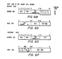
- the IOLD, function code '09' and '0D', Figs. 6A, 6C loads a 24/32-bit address into the address register associated with the referenced channel (device).
- the address refers to the starting byte location in the main memory 202 where the UPC commences input or output data transfers.
- Bits A through H, Fig. 6A are the Extended Address (bits) and bits 0 through 7 are the most significant byte of the most significant word (MSW) of the 32 bit, double word, memory byte address.
- MSW most significant word
- Fig. 6B The least significant word (LSW), Fig. 6B, of the memory byte address is contained in the data bits 0 through 15.
- Data transfers to or from memory are normally either word wide or double word wide, dependent on the UPC position on the Megabus, but byte mode transfers can occur associated with the first and/or last memory cycle of a particular data transfer if the main memory buffer (identified by this instruction) begins or ends on an odd byte boundary.
- Bit 17 of the address bus determines the direction of any subsequent data transfer operation.
- a logical One specifies an output operation (writing on medium) while a logical Zero specifies an input operation (reading from medium).
- IOLD function code '39 and '3D, Figs. 6A, 6C is used for initiating a bootstrap record load from a data storage device such as diskette, 413A, 411B, magnetic tape 408A-409A, 408B-409B, 400B, etc.
- the resident device Ramware positions an actuator to read the very first record of a storage medium and transfer it to main memory at the address specified in the instruction.
- IOLD function code '09' and '0D', Figs. 6A, 6C instruction loads the range register associated with the referenced channel.
- the unsigned, 16-bit, quantity loaded (data bus) is the number of bytes (range) to be transmitted during the data transfer that is being set up. The number is a positive binary quantity and is decremented by the UPC 201 after each memory transfer.
- the function code 0D is also a Go Function for printer adapters. A range of Zero results in a premature end-of-operation termination for any read or write command that may be subsequently issued. Any range register residue is applied to the next command unless reset by another IOLD instruction.
- the '2D' function code triggers the Ramware load procedure within the UPC or the channel, dependent on the UPC status; this action continues for successive IOLD commands until terminated by the '01', stop I/O function code, Figs. 6G, 6H and data #1000 command.
- IOLD function code '39' and '3D', Figs. 6A, 6C is used for initiating a bootstrap record load from a data storage device with a fixed range, by the controller Ramware, dependent on the device from which the data is being requested.
- the '3D' function code triggers the bootstrap load procedure within the channel.
- the default range data word transferred with the instruction contains #0000 value when the command is initiated by the SMF/software but the word can contain device specific information when the command is modified from the system control panel which further defines how the data is to be accessed. In the latter case bit significance is defined by the controller EPS; i.e., for a disk device with both a fixed and a removable medium, the range word may be interpreted as a configuration word A.
- This instruction loads Configuration Words A, B, C or D for the devices corresponding to the referenced channel. Parameters loaded are device specific indicated by bits 0-15 on Fig. 6F. Bits 8-17 identifies the device channel number; whereas bits A-H, 0-7 and 16-31 must be zero (MBZ).
- This instruction loads a control word, Fig. 6B, into the referenced channel.
- Bits A-H, 0-7 are the most significant bytes (MSB).
- Bits 8-17 identify the device channel number, and bits 18-23 are the function code bits.
- a command is invoked that causes the UPC to reset to the same state that it enters after the true power on, BSPWON (positive transition). There is no need to reload the operating Ramware.
- Another initialize command received on another channel on the UPC is accepted and executed like a new command since all of its channels are initialized, regardless of which channel the command is received over.
- This command causes any operation currently active on a specified channel to be abruptly terminated. If a data transfer operation is in progress, it is not completed and no error checking is done. An interrupt is generated (if interrupt level is not Zero) for the operation terminated by this command as if the operation ended normally. Status, address and range information, present in the UPC/channel when this command is received, is retained.
- This command causes the controller 204 and connected adapters 213 to perform extended QLT (EXQLT) diagnostics and on detection of a failure setting the QLTI byte to report a particular failing hardware identified by a unique bit pattern.
- EXQLT extended QLT
- This command terminates a successive string of IOLD ('29' and '2D') instructions to the UPC or a channel indicating the end of a Ramware load.
- the UPC determines if all the channels have their Ramware loaded; if all channels are loaded, the UPC sets an appropriate status and executes Extended QLT's (EXQLT) as under Initialize above.
- EXQLT Extended QLT's
- This command terminates an unsuccessful attempt at loading Ramware into the UPC or an adapter by the SMF or software routine; it is unable to find the medium from which to load or it is unable to load appropriate Ramware revision (SMF or software defaults to the latest Ramware revision if not exact match is found).
- SMF or software defaults to the latest Ramware revision if not exact match is found.
- the most significant bit in the adapter ID or all UPC connected adapter ID's, if UPC cannot be loaded, must be reset, to allow the SMF or software to ignore that facility.
- This command should be preceded by an 'initialize' to terminate all UPC and adapter activity for no 'task' can be active on another channel during the reload procedure.
- Extended QLT's are run on the UPC and all connected adapters after the Ramware reload is complete. The command is not valid before Ramware is loaded.
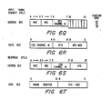
- This instruction causes the current contents of the referenced channel's memory byte address to be transferred to the requesting CSS channel.
- Bits A-H, 0-7, Fig. 6I, must be zero (MBZ).
- Bits 8-17 identify the device channel number; and bits 18-23 are the function code bits.
- the UPC During the response cycle (Figs. 6K, 6L, (second half read), the UPC returns, in bits 8 through 23 of the address bus, the same data that was received in bits 0 through 15 of the data bus during the request cycle.
- the data bus contains the Least Significant Word (LSW) of the Memory Byte Address currently stored for the specified channel in the UPC.
- FC #08 reads an address loaded by the IOLD '09'
- FC #38 reads an address loaded by the IOLD '39'. Both IOLD's '29' and '39' trigger a specific action in a controller.
- This instruction causes the current contents of the referenced channel's memory module address to be transferred to the requesting CSS channel.
- the UPC During the response cycle (second half read), the UPC returns, in bits 8 through 23 of the address bus, the same data that was received in bits 0 through 15 of the data bus during the request cycle.
- the data bus contains the most significant word (MSW) 16 bits of the memory byte address, consisting of one byte of the extended address and one byte of the most significant byte (MSB) of the memory byte address, currently stored for the specified channel in the UPC.
- MSW most significant word
- FC #2A reads an address loaded by the IOLD '29'
- FC #3A reads an address loaded by the IOLD '39'. Both IOLD's '29' and '39' trigger specific action in a controller.
- This instruction causes the current contents of the referenced channel's range register to be transferred to the requesting CSS channel.
- FC #0C reads an address loaded by the IOLD '09'
- FC #2C reads an address loaded by the IOLD '29'
- FC #3C reads an address loaded by the IOLD '39'. Both IOLD's '29' and '39 trigger a specific action in the controller.
- the contents of the range register reflect the byte count of the data transferred: If the content value is greater than zero, the length of the transfer was less than the original range. If the content is zero, the length of the transfer was equal to or greater than the original range.
- This instruction causes the current contents of the channel's Configuration Words A, B, C or D to be transferred to the requesting CSS channel.
- the UPC returns, in bits 8 through 23 of the address bus, the same data that was received in bits 0 through 15 of the data bus during the request cycle.
- This instruction causes the referenced channel's Ramware Load Status to be transferred to the requesting CSS channel.
- the UPC During the response cycle (second half read), the UPC returns, in bits 8 through 23 of the address bus, the same data that was received in bits 0 through 15 of the data bus during the request cycle.
- This bit is set whenever the UPC detects a parity error on any byte of the data, command or address during any bus cycle originated by the UPC on the first try.
- This bit is reset by an Initialize command, next Task Word command, an Input Ramware Load Status command or Master Clear on the Megabus.
- This bit indicates that, during the previous data transfer operation, main memory detected and corrected a read error.
- the data delivered to the UPC is assumed to be correct.
- This bit is reset by an Initialize command, next Task Word command, an Input Ramware Load Status command or Master Clear on the Megabus.
- This bit is reset by an Initialize command, next Task Word command, an Input Ramware Load Status command or Master Clear on the Megabus.
- This bit is set whenever the UPC detects a parity error on any byte of the local UPC memory (RAM) data.
- This bit is reset by an Initialize command, next Task Word command, an Input Ramware Load Status command or Master Clear on the Megabus.
- This bit is reset by an Initialize command, next Task Word command, an Input Ramware Load Status command or Master Clear on the Megabus.
- This bit is set on detection of a parity error in a data transferred between the UPC and an adapter.
- This bit is reset by an Initialize command, next Task Word command, an Input Ramware Load Status command or Master Clear on the Megabus.
- This bit is set when an attempt is made by software to execute the Boot IOLD '39' command to an adapter not capable of responding properly.
- This bit is reset by an Initialize command, next Task Word command, an Input Ramware Load Status command or Master Clear on the Megabus.
- This bit when set to one, indicates that the addressed channel Ramware cannot be loaded and that the channel ID is changed from '8000 + ID' to ID to enable the SMF to ignore that UPC (and all of its channels) or a channel in system configuration.
- This bit is reset by the true Power On or by the reload command.
- This bit when set to one, indicates that the UPC motherboard Ramware is loaded correctly.
- This bit is reset by the true Power On or by the reload command.
- This bit when set to one, indicates that the addressed channel Ramware is loaded correctly.
- This bit is reset by the true Power On or by the reload command.
- This bit when set to one, indicates that the Ramware just loaded was in error.
- the error condition is an OR function of the UPC and Megabus (Status Word 1 bits 13, 14 and 15) syndrome that would prevent proper operation.
- This bit is reset by an Initialize command, next Task Word command, an Input Ramware Load Status command or Master Clear on the Megabus.
- the adapter Ramware revision level is represented by a hex number, e.g. 0C, which is the sequential control number loaded during the execute QLT command after the Ramware Load.
- Adapter hardware revision level is obtained from the PROM 302 or a set of jumpers which is updated with every hardware change on the adapter.
- the revision level is to be available to the SMF or a software routine for Ramware Load procedure.
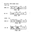
- the Address bus and Data bus of the request cycle perform similar type functions as Figs. 6I, 6J except that the function code bits 18-23 are different.
- the address bus of response cycle Fig. 7G is similar to Figs. 6K, 6O.
- the data bus Fig. 7H has the adapter hardware revision level at bits 0-7, 8-15; whereas bits 16-31 are reserved for future use (RFU) and must be zero (MBZ).
- the UPC Ramware revision level is represented by a hex number, e.g. 0D, which is the sequential control number loaded during the EXQLT command after the Ramware Load.
- UPC hardware revision level is obtained from an EPROM or a set of jumpers which is updated with every hardware change on the UPC.
- the revision level is available to the SMF or a software routine for Ramware Load procedure.
- Figs. 7I, 7J, 7K, 7L are similar to Figs. 7E, 7F, 7G, 7H, except that bits 18-23 Fig 7I are different than the bits 18-23 of 7E, but perform a similar function of identifying the function code FC for both instructions.
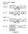
- Figs. 7M, 7N, 7O are similar to Figs. 7I, 7J, 7K.
- the UPC channel configuration, available on the base channel only, Fig. 7P appears as a series of 1's signifying an active channel an 0's signifying an inactive channel.
- the UPC maintains 32 registers (16 bits per register) for each channel.
- the address of each of the various registers in the UPC is a combination of 3 bits of the Channel Number and the high order five bits of the Function Code used to write into or read from a particular register (see Table I).
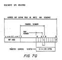
- An output bus sequence addressed to one of the devices causes the information on the data bus (16 bits) to be loaded into the device specific register specified by the device port number and the high order 5 bits of the function code, Fig. 7Q.
- the Output Address command is a special case.
- the UPC register 04 (hex) is loaded with the low order 16 bits of the address.
- the high order 16 bits of the UPC register 05 are loaded with the high order 16 bits of the address.
- Any input bus sequence addressed to a device causes the register specified by bits 14, 15 and 16 and the high order 5 bits of the Function Code to be returned via the data bus (during the second half read cycle).
- Appendix A is typical Ramware for adapter 1. Ramware for other adapters are similar except for minor details.
Landscapes
- Engineering & Computer Science (AREA)
- Theoretical Computer Science (AREA)
- Computer Hardware Design (AREA)
- Physics & Mathematics (AREA)
- General Engineering & Computer Science (AREA)
- General Physics & Mathematics (AREA)
- Software Systems (AREA)
- Bus Control (AREA)
- Multi Processors (AREA)
- Stored Programmes (AREA)
Applications Claiming Priority (2)
| Application Number | Priority Date | Filing Date | Title |
|---|---|---|---|
| US925431 | 1986-10-31 | ||
| US06/925,431 US4803623A (en) | 1986-10-31 | 1986-10-31 | Universal peripheral controller self-configuring bootloadable ramware |
Publications (2)
| Publication Number | Publication Date |
|---|---|
| EP0273136A2 true EP0273136A2 (de) | 1988-07-06 |
| EP0273136A3 EP0273136A3 (de) | 1989-10-25 |
Family
ID=25451721
Family Applications (1)
| Application Number | Title | Priority Date | Filing Date |
|---|---|---|---|
| EP87115987A Withdrawn EP0273136A3 (de) | 1986-10-31 | 1987-10-30 | Universelles Peripheriesteuerungsmodul mit Konfigurationsladung während der Initialisierung |
Country Status (3)
| Country | Link |
|---|---|
| US (1) | US4803623A (de) |
| EP (1) | EP0273136A3 (de) |
| AU (1) | AU594209B2 (de) |
Cited By (10)
| Publication number | Priority date | Publication date | Assignee | Title |
|---|---|---|---|---|
| EP0351961A3 (de) * | 1988-07-22 | 1990-08-22 | International Business Machines Corporation | Automatische Rekonfigurierungsvorrichtung |
| FR2645989A1 (fr) * | 1989-04-17 | 1990-10-19 | Bull Sa | Coupleur multifonctions entre une unite centrale d'ordinateur et les differents organes peripheriques de ce dernier |
| FR2648588A1 (fr) * | 1989-06-20 | 1990-12-21 | Commissariat Energie Atomique | Systeme de couplage avec interface entre au moins deux appareils electroniques ayant des bus d'acces de format different |
| EP0364115A3 (de) * | 1988-10-14 | 1991-03-13 | Compaq Computer Corporation | Dynamisch konfigurierbares tragbares Rechnersystem |
| EP0373849A3 (de) * | 1988-12-12 | 1991-08-07 | Diesel Kiki Co. Ltd. | Automatisches Steuerungssystem für Getriebe |
| FR2657983A1 (fr) * | 1990-02-08 | 1991-08-09 | Imecom | Carte enfichable formant controleur d'imprimante et convertisseur de donnees pour micro-ordinateur. |
| EP0528773A1 (de) * | 1991-08-09 | 1993-02-24 | Tower Tech S.R.L. | System zur dynamischen Durchführung der Konfiguration von Erweiterungskarten in Personalcomputern mit einem Standard-Bus |
| FR2701133A1 (fr) * | 1993-02-04 | 1994-08-05 | Gemplus Card Int | Procédé de communication avec un support portatif. |
| WO1998012647A1 (en) * | 1996-09-23 | 1998-03-26 | International Business Machines Corporation | Interface for a split system personal computer |
| GB2520725A (en) * | 2013-11-29 | 2015-06-03 | St Microelectronics Res & Dev | Circuitry for configuring entities |
Families Citing this family (45)
| Publication number | Priority date | Publication date | Assignee | Title |
|---|---|---|---|---|
| US5564110A (en) * | 1987-03-10 | 1996-10-08 | Canon Kabushiki Kaisha | Printer interface apparatus with plug-in unit authorized for reception of data upon type verification |
| JP2753706B2 (ja) * | 1987-12-09 | 1998-05-20 | 富士通株式会社 | 計算機におけるipl方法 |
| JPH01248256A (ja) * | 1988-03-30 | 1989-10-03 | Toshiba Corp | 入出力制御方式 |
| JP2664950B2 (ja) * | 1988-08-31 | 1997-10-22 | 日本電気株式会社 | 入出力処理装置 |
| US5257387A (en) * | 1988-09-09 | 1993-10-26 | Compaq Computer Corporation | Computer implemented method and apparatus for dynamic and automatic configuration of a computer system and circuit boards including computer resource allocation conflict resolution |
| US5247659A (en) * | 1988-10-06 | 1993-09-21 | International Computers Limited | Method for bootstrap loading in a data processing system comprising searching a plurality of program source devices for a bootstrap program if initial data indicating a bootstrap program source device fails a validity check |
| US5214762A (en) * | 1988-11-07 | 1993-05-25 | Compaq Computer Corporation | Disk drive activity indicator |
| US5101490A (en) * | 1989-01-10 | 1992-03-31 | Bull Hn Information Systems Inc. | Peripheral device controller with an EEPROM with microinstructions for a RAM control store |
| EP0393290B1 (de) * | 1989-04-19 | 1995-08-16 | International Business Machines Corporation | Anordnung zur Speicher- und Peripherie-Bausteinauswahl |
| US5119498A (en) * | 1989-06-12 | 1992-06-02 | International Business Machines Corporation | Feature board with automatic adjustment to one of two bus widths based on sensing power level at one connection contact |
| US5210854A (en) * | 1989-06-14 | 1993-05-11 | Digital Equipment Corporation | System for updating program stored in eeprom by storing new version into new location and updating second transfer vector to contain starting address of new version |
| US5319770A (en) * | 1989-10-03 | 1994-06-07 | International Business Machines Corporation | Data processing method and apparatus for verifying adapter description file choices |
| JP2629384B2 (ja) * | 1989-11-16 | 1997-07-09 | 日本電気株式会社 | ダウンラインロード起動制御方式 |
| US5247671A (en) * | 1990-02-14 | 1993-09-21 | International Business Machines Corporation | Scalable schedules for serial communications controller in data processing systems |
| FR2658934B1 (fr) * | 1990-02-28 | 1992-04-30 | Bull Sa | Architecture de systeme et utilisation de cette architecture dans un procede de remplacement de cartes. |
| FR2663137B1 (fr) * | 1990-06-12 | 1994-07-29 | Sgs Thomson Microelectronics | Dispositif electronique de connexion. |
| US5446877A (en) * | 1990-11-13 | 1995-08-29 | Nakamichi Peripherals Corporation | Method and apparatus for operation of a data archival apparatus allowing for coupling of the data archival device with an ide interface |
| DE69130667T2 (de) * | 1990-12-06 | 1999-05-06 | Tandberg Data Asa, Oslo | Datenspeicherungssystem mit auswechselbaren Medien zum Laden eines Steuerprogrammes von den auswechselbaren Medien |
| JP2637310B2 (ja) * | 1991-06-19 | 1997-08-06 | 富士通株式会社 | システムインストール制御装置 |
| US5619701A (en) * | 1992-01-23 | 1997-04-08 | International Business Machines Corporation | Method and system for adapter configuration in a data processing system |
| US5574869A (en) * | 1992-03-30 | 1996-11-12 | Intel Corporation | Bus bridge circuit having configuration space enable register for controlling transition between various modes by writing the bridge identifier into CSE register |
| IL105638A0 (en) * | 1992-05-13 | 1993-09-22 | Southwest Bell Tech Resources | Storage controlling system and method for transferring information |
| DE4229931C2 (de) * | 1992-09-08 | 1997-01-23 | Daimler Benz Ag | Verfahren zur Programmierung eines busfähigen elektronischen Kfz-Steuergerätes |
| US5996027A (en) * | 1992-12-18 | 1999-11-30 | Intel Corporation | Transmitting specific command during initial configuration step for configuring disk drive controller |
| US5537607A (en) * | 1993-04-28 | 1996-07-16 | International Business Machines Corporation | Field programmable general purpose interface adapter for connecting peripheral devices within a computer system |
| US5581766A (en) * | 1993-05-17 | 1996-12-03 | Compaq Computer Corporation | Selectable video driver system |
| US5644790A (en) * | 1994-02-16 | 1997-07-01 | Ati Technologies, Inc. | Universal CD ROM interface using single interface connection |
| US5551053A (en) * | 1994-02-28 | 1996-08-27 | Eaton Corporation | System and Method for assigning addresses to I/O devices in a control network and for verifying the assigned address of the devices |
| JPH07271699A (ja) * | 1994-03-31 | 1995-10-20 | Canon Inc | ネットワークを介して接続される周辺処理装置と情報処理装置並びにその周辺処理装置における制御方法とその周辺処理装置の制御方法 |
| US5586327A (en) * | 1994-09-27 | 1996-12-17 | International Business Machines Corporation | Extended initialization for personal data processing systems |
| US5699350A (en) * | 1995-10-06 | 1997-12-16 | Canon Kabushiki Kaisha | Reconfiguration of protocol stacks and/or frame type assignments in a network interface device |
| US5732283A (en) * | 1995-10-24 | 1998-03-24 | International Business Machines Corporation | System and method of providing universal support for multiple pointing devices |
| KR0167644B1 (ko) * | 1995-11-30 | 1999-02-01 | 김광호 | 다수의 통신 전송 방식을 선택적으로 사용하기 위한 통신시스템 |
| US5768294A (en) * | 1995-12-11 | 1998-06-16 | International Business Machines Corporation | Memory implemented error detection and correction code capable of detecting errors in fetching data from a wrong address |
| US5819050A (en) * | 1996-02-29 | 1998-10-06 | The Foxboro Company | Automatically configurable multi-purpose distributed control processor card for an industrial control system |
| US5923897A (en) * | 1996-04-01 | 1999-07-13 | Microsoft Corporation | System for adapter with status and command registers to provide status information to operating system and processor operative to write eject command to command register |
| US5854942A (en) * | 1996-09-06 | 1998-12-29 | International Business Machines Corporation | Method and system for automatic storage subsystem configuration |
| US6249826B1 (en) | 1997-04-14 | 2001-06-19 | Microsoft Corporation | System and method for media status notification |
| US6175770B1 (en) | 1997-12-31 | 2001-01-16 | Dana Corporation | Electronic controller having automatic self-configuration capabilities |
| US6145020A (en) * | 1998-05-14 | 2000-11-07 | Advanced Technology Materials, Inc. | Microcontroller incorporating an enhanced peripheral controller for automatic updating the configuration date of multiple peripherals by using a ferroelectric memory array |
| US6378049B1 (en) | 1998-11-16 | 2002-04-23 | Infineon Technologies A.G. | Universal memory controller |
| US6532505B1 (en) | 1999-11-12 | 2003-03-11 | Infineon Technologies Ag | Universal resource access controller |
| WO2000029955A1 (en) * | 1998-11-16 | 2000-05-25 | Infineon Technologies Ag | Universal resource access controller |
| US7684875B2 (en) * | 2007-02-02 | 2010-03-23 | Fisher-Rosemount Systems, Inc. | Methods and apparatus to configure process control system inputs and outputs |
| US10585673B2 (en) | 2015-02-10 | 2020-03-10 | Hewlett Packard Enterprise Development Lp | Chipset reconfiguration based on device detection |
Family Cites Families (10)
| Publication number | Priority date | Publication date | Assignee | Title |
|---|---|---|---|---|
| US3427593A (en) * | 1966-03-24 | 1969-02-11 | Burroughs Corp | Data processor with improved program loading operation |
| CA1081855A (en) * | 1976-04-29 | 1980-07-15 | David B. Schuck | Initializing means for a bus-oriented data processing system employing firmware-configured modules |
| US4070704A (en) * | 1976-05-17 | 1978-01-24 | Honeywell Information Systems Inc. | Automatic reconfiguration apparatus for input/output processor |
| US4191996A (en) * | 1977-07-22 | 1980-03-04 | Chesley Gilman D | Self-configurable computer and memory system |
| US4491916A (en) * | 1979-11-05 | 1985-01-01 | Litton Resources Systems, Inc. | Large volume, high speed data processor |
| US4400778A (en) * | 1979-11-05 | 1983-08-23 | Litton Resources Systems, Inc. | Large-volume, high-speed data processor |
| JPS57176456A (en) * | 1981-04-22 | 1982-10-29 | Fanuc Ltd | Data processing system |
| US4562533A (en) * | 1981-12-03 | 1985-12-31 | Ncr Corporation | Data communications system to system adapter |
| DE3381881D1 (de) * | 1983-02-22 | 1990-10-18 | Ibm | Verfahren zur dynamischen rekonfiguration eines datenverarbeitungssystems bei hinzufuegung von einrichtungen. |
| US4701845A (en) * | 1984-10-25 | 1987-10-20 | Unisys Corporation | User interface processor for computer network with maintenance and programmable interrupt capability |
-
1986
- 1986-10-31 US US06/925,431 patent/US4803623A/en not_active Expired - Lifetime
-
1987
- 1987-10-30 EP EP87115987A patent/EP0273136A3/de not_active Withdrawn
- 1987-11-02 AU AU80612/87A patent/AU594209B2/en not_active Ceased
Cited By (17)
| Publication number | Priority date | Publication date | Assignee | Title |
|---|---|---|---|---|
| EP0351961A3 (de) * | 1988-07-22 | 1990-08-22 | International Business Machines Corporation | Automatische Rekonfigurierungsvorrichtung |
| EP0364115A3 (de) * | 1988-10-14 | 1991-03-13 | Compaq Computer Corporation | Dynamisch konfigurierbares tragbares Rechnersystem |
| EP0373849A3 (de) * | 1988-12-12 | 1991-08-07 | Diesel Kiki Co. Ltd. | Automatisches Steuerungssystem für Getriebe |
| FR2645989A1 (fr) * | 1989-04-17 | 1990-10-19 | Bull Sa | Coupleur multifonctions entre une unite centrale d'ordinateur et les differents organes peripheriques de ce dernier |
| EP0394114A1 (de) * | 1989-04-17 | 1990-10-24 | Bull S.A. | Multifunktionskoppler zwischen einer zentralen Verarbeitungseinheit eines Rechners und verschiedenen Peripheriegeräten dieses Rechners |
| FR2648588A1 (fr) * | 1989-06-20 | 1990-12-21 | Commissariat Energie Atomique | Systeme de couplage avec interface entre au moins deux appareils electroniques ayant des bus d'acces de format different |
| EP0404653A1 (de) * | 1989-06-20 | 1990-12-27 | Commissariat A L'energie Atomique | Kopplungssystem mit einer Schnittstelle zwischen mindestens zwei elektronischen Geräten mit verschiedenen Formatzugriffbussen |
| EP0441699A1 (de) * | 1990-02-08 | 1991-08-14 | Imecom | Kontrollgerät für einen Drucker und Datenkonverter für Mikrocomputer |
| FR2657983A1 (fr) * | 1990-02-08 | 1991-08-09 | Imecom | Carte enfichable formant controleur d'imprimante et convertisseur de donnees pour micro-ordinateur. |
| EP0528773A1 (de) * | 1991-08-09 | 1993-02-24 | Tower Tech S.R.L. | System zur dynamischen Durchführung der Konfiguration von Erweiterungskarten in Personalcomputern mit einem Standard-Bus |
| FR2701133A1 (fr) * | 1993-02-04 | 1994-08-05 | Gemplus Card Int | Procédé de communication avec un support portatif. |
| WO1994018628A1 (fr) * | 1993-02-04 | 1994-08-18 | Gemplus Card International | Procede de communication avec un support portatif |
| US5651116A (en) * | 1993-02-04 | 1997-07-22 | Gemplus Card International | Method and apparatus for generating summaries of prepaid instrument transaction activity |
| WO1998012647A1 (en) * | 1996-09-23 | 1998-03-26 | International Business Machines Corporation | Interface for a split system personal computer |
| GB2520725A (en) * | 2013-11-29 | 2015-06-03 | St Microelectronics Res & Dev | Circuitry for configuring entities |
| US9645830B2 (en) | 2013-11-29 | 2017-05-09 | Stmicroelectronics (Research & Development) Limited | On-chip circuitry for configuring peripherals of a system on a chip |
| US10180847B2 (en) | 2013-11-29 | 2019-01-15 | Stmicroelectronics (Research & Development) Limited | Circuitry for configuring entities |
Also Published As
| Publication number | Publication date |
|---|---|
| AU594209B2 (en) | 1990-03-01 |
| US4803623A (en) | 1989-02-07 |
| AU8061287A (en) | 1988-05-05 |
| EP0273136A3 (de) | 1989-10-25 |
Similar Documents
| Publication | Publication Date | Title |
|---|---|---|
| US4803623A (en) | Universal peripheral controller self-configuring bootloadable ramware | |
| US5499346A (en) | Bus-to-bus bridge for a multiple bus information handling system that optimizes data transfers between a system bus and a peripheral bus | |
| US5115499A (en) | Shared computer resource allocation system having apparatus for informing a requesting computer of the identity and busy/idle status of shared resources by command code | |
| EP0591437B1 (de) | Verteilte multiprozessor-initialisierung und selbstprüfungssystem | |
| US4870566A (en) | Scannerless message concentrator and communications multiplexer | |
| US4453211A (en) | System bus for an emulated multichannel system | |
| CA1064623A (en) | Programmable interface apparatus and method | |
| US4133030A (en) | Control system providing for the transfer of data in a communications processing system employing channel dedicated control blocks | |
| US5729767A (en) | System and method for accessing peripheral devices on a non-functional controller | |
| US3996564A (en) | Input/output port control | |
| US4495571A (en) | Data processing system having synchronous bus wait/retry cycle | |
| US5038320A (en) | Computer system with automatic initialization of pluggable option cards | |
| US4354225A (en) | Intelligent main store for data processing systems | |
| KR970000842B1 (ko) | 정보 처리 시스템 및 컴퓨터 시스템 | |
| US4488231A (en) | Communication multiplexer having dual microprocessors | |
| US4300193A (en) | Data processing system having data multiplex control apparatus | |
| US4484271A (en) | Microprogrammed system having hardware interrupt apparatus | |
| US4317169A (en) | Data processing system having centralized memory refresh | |
| US4261033A (en) | Communications processor employing line-dedicated memory tables for supervising data transfers | |
| EP0139563B1 (de) | Steuermechanismus für Mehrprozessorsystem | |
| WO1998000783A1 (en) | Method and apparatus for power management of distributed direct memory access (ddma) devices | |
| US5146605A (en) | Direct control facility for multiprocessor network | |
| US4509115A (en) | Two-port memory controller | |
| US4400772A (en) | Method and apparatus for direct memory access in a data processing system | |
| HK18590A (en) | Extended addressing apparatus and method for direct storage access devices |
Legal Events
| Date | Code | Title | Description |
|---|---|---|---|
| PUAI | Public reference made under article 153(3) epc to a published international application that has entered the european phase |
Free format text: ORIGINAL CODE: 0009012 |
|
| AK | Designated contracting states |
Kind code of ref document: A2 Designated state(s): DE FR GB IT |
|
| PUAL | Search report despatched |
Free format text: ORIGINAL CODE: 0009013 |
|
| AK | Designated contracting states |
Kind code of ref document: A3 Designated state(s): DE FR GB IT |
|
| 17P | Request for examination filed |
Effective date: 19900425 |
|
| 17Q | First examination report despatched |
Effective date: 19900903 |
|
| STAA | Information on the status of an ep patent application or granted ep patent |
Free format text: STATUS: THE APPLICATION HAS BEEN WITHDRAWN |
|
| 18W | Application withdrawn |
Withdrawal date: 19910108 |
|
| R18W | Application withdrawn (corrected) |
Effective date: 19910108 |
|
| RIN1 | Information on inventor provided before grant (corrected) |
Inventor name: LEWIS, RICHARD P. Inventor name: MCNAMARA, JOHN L. Inventor name: KOWAL, KRZYSZTOF A. Inventor name: KAUFMAN, SIDNEY L. Inventor name: RAISBECK, SUSAN L. Inventor name: KLASHKA, JOHN A. |