EP0268447A2 - Schaltung für die Analyse des Frequenzverhaltens - Google Patents
Schaltung für die Analyse des Frequenzverhaltens Download PDFInfo
- Publication number
- EP0268447A2 EP0268447A2 EP87310105A EP87310105A EP0268447A2 EP 0268447 A2 EP0268447 A2 EP 0268447A2 EP 87310105 A EP87310105 A EP 87310105A EP 87310105 A EP87310105 A EP 87310105A EP 0268447 A2 EP0268447 A2 EP 0268447A2
- Authority
- EP
- European Patent Office
- Prior art keywords
- analogue
- signal
- digital
- frequency response
- converter
- Prior art date
- Legal status (The legal status is an assumption and is not a legal conclusion. Google has not performed a legal analysis and makes no representation as to the accuracy of the status listed.)
- Granted
Links
Images

Classifications
-
- G—PHYSICS
- G01—MEASURING; TESTING
- G01R—MEASURING ELECTRIC VARIABLES; MEASURING MAGNETIC VARIABLES
- G01R27/00—Arrangements for measuring resistance, reactance, impedance, or electric characteristics derived therefrom
- G01R27/28—Measuring attenuation, gain, phase shift or derived characteristics of electric four pole networks, i.e. two-port networks; Measuring transient response
-
- G—PHYSICS
- G01—MEASURING; TESTING
- G01R—MEASURING ELECTRIC VARIABLES; MEASURING MAGNETIC VARIABLES
- G01R23/00—Arrangements for measuring frequencies; Arrangements for analysing frequency spectra
- G01R23/16—Spectrum analysis; Fourier analysis
Definitions
- This invention relates to frequency response analysis.
- Such analysis in which the input signal applied to a system is compared with the output signal from the system at various frequencies, is a well-known technique for characterising the behaviour of, for example, servo systems, rotating machinery, electrical and electronic circuits and elastic and viscous materials.
- the output signal is often analysed by correlating it with reference signals which are in phase and in quadrature phase with the input signal to the system.
- the input signal to the system might be a sine wave and the correlation process involve identifying the components of a return signal from the system under test at the frequency of the input sine wave and at harmonics thereof.
- the frequency of the input may be swept between limits defining a band of frequencies of interest, and measurements made within the sweep to further characterise the system.
- the instantaneous value of a component that might be present in a return signal is seldom of interest, and the average value is the prefered measurement.
- Averaging is known in other areas of instrumentation, for example in integrating analogue to digital converters. Such devices serve to provide a numeric output representative of the average value of a signal applied to a device input during an averaging period.
- Such techniques as dual slope integration and the pulse with conversion technique described in United Kingdom Patent No. 1 434 414 are well documented elsewhere and do not require further description here.
- Also well known in the instrumentation art is the process of digital to analogue conversion, that is of providing an analogue signal having an instantaneous value representative of the numeric value of a digital input applied to a converter.
- a second input may be applied in analogue form, resulting in an output which has the value of the analogue input multiplied by the value of the digital input.
- Such devices are termed multiplying digital to analogue converters, and these too are adequately described elsewhere.
- a frequency response analyser includes a signal generator for providing a periodic driving signal, means for relaying the driving signal to a system under test, means for receiving an output signal from a system under test, means for deriving a reference signal of digital form, a multiplying digital to analogue converter having an analogue input, a digital input and an analogue output, the analogue input being connected to receive said output signal and the digital input being connected to said reference signal, and an integrating analogue to digital converter arranged to convert the output of the multiplying digital to analogue converter over an integral number of periods of the driving signal.
- said reference signal varies as a sine function of the same period as the driving signal and a second multiplying digital to analogue converter is arranged to multiply the output signal by a second reference signal which varies as a cosine function of the same period as the driving signal, a second integrating analogue to digital converter being arranged to convert the ouput of the second multiplying digital to analogue converter over an integral number of periods of the driving signal.
- said reference signal may vary as a first reference function during a first period to establish a firszt characterising coefficient and may vary as a second reference function during a second period to establish a second characterising co-efficient.
- the multiplying digital to analogue converter may be of the one quadrant type, and means included to add in a dc level to the analogue input, the reference signal arranged to vary as a function of (1 + sine), and means included to subtract a related dc level intermediate the multiplying digital to analogue converter and integrating analogue to digital converter.
- a dc level may be added to the analogue input of a second multiplying digital to analogue converter receiving a signal varying as a function of (1+ cosine) at its digital input, and means included intermediate the second multiplying digital to analogue converter and a second integrating analogue to digital converter to subtract a related dc level.
- the multiplying digital to analogue converter may be of the two quadrant type, allowing its analogue input to be of either polarity. Sign variation of the reference signal may be accomodated by arranging for the analogue input to be inverted whenever the reference signal should take on a negative value.
- a second multiplying digital to analogue converter of the two quadrant type may be similarly arranged with respect to a second reference signal.
- a first reference function and a second reference function may be sequentially applied to a single multiplying digital to analogue converter.
- the means for deriving the reference signal includes a memory device, having values of the required reference function stored therein, for example sine or cosine or (1 + sine) or (1 + cosine). Additionally the memory may be arranged to store values of the harmonics of the required function so that harmonics of the reference signal may be used in correlation.
- demodulation may be achieved by rectifying the received signal to one polarity during a first half cycle of the carrier period, and to the other polarity during the second half cycle.
- a polarity switch connected to selectively invert the received signal is included and controlled to invert the output signal at every alternate half cycle of the carrier to give rectification as aforesaid prior to connection to the multiplying digital to analogue converter.
- the polarity of the reference signal may be switched, preferably, where the reference is derived from memory, by selectively addressing samples of an inverse reference function stored in memory together with the reference signal samples.
- a drive signal is generated to be available as an input signal to a sytem under test 10.
- An output signal is derived from the system under test 10 by means not shown but which might for example comprise an accelerometer or other transducer for reception at a connection point 11 of the frequency response analyser.
- the drive signal is derived from a read only memory (ROM) 12 which is addressed by the multiple digital outputs of a counter 14.
- the ROM 12 contains samples of a sinusoidal waveform arranged in order such that when sequentially addressed and d/a converted a sinusoidal drive signal is present at the output of the amplifier 16.
- the frequency of the drive signal is determined by the frequency of a clock 17, which clocks the counter 14.
- the signal received from the system under test is relayed to the analogue input of a multiplying digital to analogue converter 18.
- the digital input for the multiplying digital to analogue converter 18 is derived from a ROM 19, which is addressed by the data output lines of counter 14 in a way analoguous to the ROM 12.
- the ROM 19 is arranged to contain sequential samples of a reference signal, which in this embodiment is a sine wave, to derive a signal in digital form which is connected to the digital input of the multiplying digital to analogue converter 18 as described above.
- the multiplying digital to analogue converter 18 provides an analogue output 100 which is relayed to an integrating analogue to digital converter 101 to give a digital output 102.
- the addressing of the ROM 12 by the data output of the counter 14 leads to a sinusoid of an angular frequency w and of amplitude A appearing at the output of the amplifier 16.
- the driving signal may be represented as A sin wt.
- the received signal at input 11 will generally not be of this form, but may contain many components of varying instantaneous amplitude.
- a typical objective of frequency response analysis might be to establish the level of the components (a1, b1) at the fundamental frequency present in the signal from the system under test following application of the driving signal.
- the function of a multiplying digital to analogue converter is to multiply the instantaneous values of signals applied to its analogue and digital inputs, and to provide an analogue value representative of the result.
- B, ⁇ and w are all either constant or known, and that thus the value of the output 102 of the integrating analogue to digital converter 101 at the end of the averaging period may be directly related to a required coefficient a1 characterising the frequency response of the system under test 10.
- a second multiplying digital to analogue converter 103 also receives the signal received from the system under test x1(t), at its analogue input.
- the digital input to this multiplying digital to analogue converter 103 is supplied from a ROM 104, addressed by the data outputs of the counter 14, in a way analogous to ROM 19, excepting that the ROM 104 is loaded with samples of a cosinusoid.
- the ROM 104 provides a reference signal C.coswt in digital form.
- Analogue output 105 of multiplying digital to analogue converter 103 may thus be represented by V(t). Ccoswt.
- the signal appearing at the output 105 is fed to an integrating analogue to digital converter 106 having a digital output 107.
- the integrating analogue to digital converter 106 is arranged to have an integrating period of one cycle of the fundamental reference waveform, that is 2 ⁇ /w.
- An analysis similar to that performed for the behaviour of multiplying digital to analogue converter 18 and integrating analogue to digital converter 101 may be performed for multiplying digital to analogue converter 103 and integrating analogue to digital converter 106.
- the output 107 of integrated analogue to digital converter 106 at the end of the averaging period may be directly related to a required coefficient b1 characterising the frequency response of the system under test 10.
- the outputs 102, 107 at the end of the averaging period may therefore be directly related to the required characterising coefficients a n , b n , respectively.
- the application of the alternative reference signals may be achieved by addressing samples of different reference waveforms stored in the ROMs 19, 104 respectively.
- Extra addressing bits are supplied from a harmonic selector 108, which is connected to some address lines of the ROMs and is arranged to select an appropriate address range, so that the samples of the required reference signal will be present at the digital outputs of the ROMs 19, 104 respectively during an addressing cycle of the counter 14.
- the ROM 19 might have fourteen address lines, the least significant ten bits being directly addressed by the counter 14, which is arranged to count from zero to 1023 to sequentially address the 1024 states definable with ten bits.
- the ROM 19 has a capacity of 16k bits. Of the remaining bits four are addressed by harmonic selector 108. For each different combination of these four address inputs, a different set of 1024 locations may be addressed. Thus for the 16k ROM, 1024 samples of sixteen different reference waveforms may be addressed. The ROM 19 is therefore loaded with samples as follows:-
- the ROM 104 may be similarly loaded with samples of the values of the functions cos wt (addresses 0 to 1023) through to cos 16 wt (addresses 15360 to 16383).
- the embodiment is arranged to operate as follows.
- the harmonic number is set to zero, and the outputs of the integrating analogue to digital converters 101, 106 are cleared.
- the clock 17 is enabled so that counter 14 counts from 0 to 1023 to simultaneously address the waveform ROM 12, and reference ROMs 19 and 104.
- references at the fundamental frequency are fed to the digital inputs of multiplying analogue to digital converters 18, 103 respectively.
- the outputs of the integrating analogue to digital converters will contain digital representations defining the characterising coefficients a1, b1, which may be stored for later processing or displayed as required.
- the outputs of the integrating analogue to digital converters may be cleared and the harmonic selector incremented by one.
- the received signal is thus correlated with reference sin 2 wt, cos 2wt to allow the second harmonic characterising coefficients a2, b2 to be determined.
- This procedure is repeated, with incremented harmonic number, until all harmonic characterising co-efficients (i.e. up to a16, b16) have been determined.
- control logic not shown, but which will be readily realisable by those skilled in the art.
- the precise operation desirable will depend upon application, and thus the control logic may vary with application. For example, in general in most applications it is best to leave the system under test 10 permanently driven, by arranging that the counter 14 is continuously cycling.
- Acquisition of any particular characterising coefficient pair may then be achieved by clearing the integrating analogue to digital converters 101, 106 in synchronism with the counter, for example by applying a clearing signal to trigger inputs 109, 110 of integrating analogue to digital converters 101, and 106 respectively.
- averaging period at 2 ⁇ /w, being that of the fundamental.
- An averaging period of a multiple of 2 ⁇ /w may be used, such a longer period having the benefit of increasing noise rejection.
- the counter 15 has a trigger signal input 111, which may, for example, reset the count to zero prior to an acquisition, and the clock 17 a synchronising input 112 so that the cycle time may be made equal to the period of an external reference.
- a trigger signal input 111 which may, for example, reset the count to zero prior to an acquisition
- the clock 17 a synchronising input 112 so that the cycle time may be made equal to the period of an external reference.
- both the signal received from the system under test and the reference signal may take both positive and negative instantaneous values during the course of a cycle.
- the multiplying digital to analogue converters 18, 103 operate in all four quadrants, ie. both the analogue and digital inputs may take positive and negative values.
- Four quadrant multipliers are not readily available, and it is preferable that a two-quadrant type be used.
- the analogue input may be of either polarity.
- the ROMs 19 and 104 contain positive values only, which may be regarded as positively rectified values of the reference waveforms.
- the signal received from the system under test 10 at input 11 is relayed to the multiplying digital to analogue converters 18, 103 via either one of a non-inverting amplifier 113, or an inverting amplifier 114, both of unity gain.
- the selection is controlled by a switch 115, and switch control logic 116, which is arranged such that whenever the reference signal stored in the ROM 19 should have a negative value, the inverting amplifier 114 is connected, the non-inverting amplifier 113 being connected at other times.
- This arrangement is effective to invert the analogue input (i.e. make it of opposite polarity) whenever the reference waveform should be negative, and effectively permits the reference to take on negative values by virtue of the commutative nature of multiplication.
- a straightforward way of providing an indication of the required inversion or non-inversion of the received signal is by storing a polarity bit together with the magnitude data for each sample of each reference waveform, which may be fed directly to a signal input 117 of switch control logic 116.
- inverting amplifier 118 non-inverting amplifier 119 and switch 122, connected intermediate the received signal input 11 and the multiplying digital to analogue converter 103 allow the converter 103 to affectively operate in four quadrants in response to a polarity signal from the ROM 104 fed to the switch control logic 120 at sign input 121.
- the driving signal is used to modulate a carrier signal of high frequency, which modulated carrier is then applied to the system under test.
- a carrier signal of high frequency which modulated carrier is then applied to the system under test.
- the components of received signal at the fundamental and harmonic frequencies of the modulating driving signal.
- the received signal must be demodulated prior to correlation.
- a signal generator 123 supplies a carrier signal which is fed to an input of an optional modulator 124.
- the other modulator input is fed with the driving signal derived from the waveform ROM 12 and the digital to analogue converter 15.
- the conditioning amplifier 16 supplies a signal to the system under test 10 having the driving signal as the modulating waveform.
- a multiplying digital to analogue converter may be used in the position of digital to analogue converter 15, its analogue input being supplied from generator 123 to thereby provide an effectively modulated output to amplifier 16.
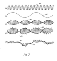
- the carrier signal is a high frequency sinusoidal, as might, for example, be diagrammatically represented by a profile 20 ( Figure 2(a)), and the modulating driving signal is a lower frequency sinusoid, 21 ( Figure 2(b)).
- the drive signal applied to the system under test will be a modulated waveform, 22 ( Figure 2(c)).
- the signal received from the system under test 10 at input 11 is of a form 23 ( Figure 2(d)), and contains frequency components for analysis as hereinbefore described.
- the received signal will be of the form of a modulated carrier, appearing as a sinusoid within an envelope 24.
- this enveloping waveform which is of interest in the analysis, and it may be recovered by switching the received signal of the form 23 with the polarity of the carrier signal for form 20 to give a signal of the form 26 ( Figure 2(e)), from which the enveloping signal 27 may be recovered in accordance with known principles of demodulation. It would be a simple matter for one skilled in the art to configure the control logic (116, 120) necessary to give the required switching and inversions.
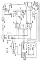
- FIG. 3 An alternative embodiment of the present invention, ( Figure 3) operates under the control of a micro-computer 30, and is arranged to operate with multiplying digital to analogue converters 31, 32, both of the one quadrant type.
- a driving signal is supplied to a system under test 33 from a digital to analogue converter 34 via an amplifier 35.
- the digital input for the digital to analogue converter 34 is derived from a ROM 36 addressed by a counter 37 controlled by a clock 38.
- the counter also addresses two further ROMs 39, 300.
- This arrangement serves to generate a driving signal and two reference signals, in a way analogous to that hereinbefore described, to permit a frequency response analysis to be carried out of the system under test 33, a signal from which is received at an input 301.
- the multiplying digital to analogue converter 31 is of the one quadrant type. This means that neither the signal which is applied to its digital input via data lines 302, nor the signal applied at its analogue input on line 303 may take on negative values. In the case of the digital input supplied from the ROM 39. Where the waveform stored can take negative values, such values may be indicated by a separate sign bit not fed to the multiplying digital to analogue converter, but used in averaging, as will be described later.
- the instantaneous value of the signal received at the input 301 may be of either polarity.
- a dc reference level 305 is added to the received signal by a summing amplifier 306.
- the magnitude of the reference of the reference level 305 is chosen in relation to the received signal such that the resulting signal, which appear an analogue input line 303, will always be of positive polarity.
- the reference signal samples loaded into the ROM 39 are of the waveform B.(1 + sin wt) and its harmonics, which may be selected by addressing harmonic select lines 307 in a way analogous to that already described.
- the instantaneous output of the multiplying digital to analogue converter 31 may be represented as:-
- this system dependent component Ba n may be applied to the input of an analogue to digital converter for integration over a period of 2 ⁇ /w (i.e. one cycle of the fundamental reference)
- the REF dc .B component is subtracted from the output signal 309 of the multiplying digital to analogue converter 31 by means of a difference amplifier 310.
- the component for subtraction by difference amplifier 310 is derived by a scaling 311 of the reference level 305.
- the only remaining dc component of the output of the multiplying digital to analogue converter 31 will be Ba n , which will be the only contributor to an integration performed over the fundamental period 2 ⁇ /w, as will be apparent from the foregoing.
- the resultant output from the different amplifier 310 is relayed to the analogue to digital converter 308 which, in this example, is not of the integrating type, but instead gives a series of instantaneous converted values on output lines 314, which are loaded into register 312.
- the register stack 312 will contain a plurality of values which may be averaged and differenced to give a numerical value representative of the value and thereby related to the value of the required co-efficient a n . Since the register stack 312 is configured within the micro-computer 30, these essentially arithmetic operations are performed therein under micro-program control. Operation of the various components thus far may be controlled by Trigger control 316, also configured within the micro-computer 30 under program control.
- the trigger control 316 serves to synchronise operation by enabling the clock 38, reseting and enabling the counter 37, and setting harmonic number via harmonic control 317 to provide a partial address on lines 307.
- the trigger may be internally generated, or may be externally supplied via an input 318 when the use of the correlator part of the frequency response analyser with an external signal generator is required.
- values may be loaded to one of two register stacks, dependent upon the polarity of the reference, for example in response to a sign bit output from reference wave ROM 39.
- the accumulated positive and negative values may then be added together and differenced to yield the required coefficient.
- the polarity switching required for demodulation may also be achieved in this way.
- the components of the emboidment thus far described serve to provide the characterising coefficients a1, a2, a n . Further analysis is performed in relation to a reference waveform C(1+cosnwt) in order to establish the remaining characterising coefficients b1, b2, b n .
- a reference dc level is added to the incoming signal by a summing amplifier 320, the output of which feeds multiplying digital to analogue converter 32.
- the reference is available in digital form from the ROM 300.
- the multiplied signal is differenced with a scaled reference (via scaler 321) by difference amplifier 322, to give an output for analogue to digital conversion by an analogue to digital converter 323, output values from which are loaded to register stack 324. These values may then be averaged and differenced by the micro-computer 30 under program control to yield the required chracterising coefficients.
- the operation of this second channel is analogous to that of the first, and analogous theory may be applied thereto, making further detailed
Landscapes
- Physics & Mathematics (AREA)
- General Physics & Mathematics (AREA)
- Mathematical Physics (AREA)
- Measurement Of Resistance Or Impedance (AREA)
- Analogue/Digital Conversion (AREA)
Applications Claiming Priority (2)
| Application Number | Priority Date | Filing Date | Title |
|---|---|---|---|
| GB8627370 | 1986-11-15 | ||
| GB8627370A GB2198246B (en) | 1986-11-15 | 1986-11-15 | Improvements in or relating to frequency response analysis |
Publications (3)
| Publication Number | Publication Date |
|---|---|
| EP0268447A2 true EP0268447A2 (de) | 1988-05-25 |
| EP0268447A3 EP0268447A3 (en) | 1989-10-18 |
| EP0268447B1 EP0268447B1 (de) | 1993-11-03 |
Family
ID=10607435
Family Applications (1)
| Application Number | Title | Priority Date | Filing Date |
|---|---|---|---|
| EP87310105A Expired - Lifetime EP0268447B1 (de) | 1986-11-15 | 1987-11-16 | Schaltung für die Analyse des Frequenzverhaltens |
Country Status (5)
| Country | Link |
|---|---|
| US (1) | US4868487A (de) |
| EP (1) | EP0268447B1 (de) |
| JP (1) | JPS63259475A (de) |
| DE (1) | DE3788040T2 (de) |
| GB (1) | GB2198246B (de) |
Cited By (4)
| Publication number | Priority date | Publication date | Assignee | Title |
|---|---|---|---|---|
| EP0321963A1 (de) * | 1987-12-23 | 1989-06-28 | Advantest Corporation | Impedanzmessgerät |
| EP0417708A3 (en) * | 1989-09-11 | 1992-01-02 | Advantest Corporation | Impedance and transfer characteristic measuring apparatus |
| WO2000020875A1 (de) * | 1998-10-05 | 2000-04-13 | Den Dulk, Gerard | Frequenzganganalysator |
| EP1200925A4 (de) * | 1998-11-30 | 2005-05-11 | Elster Electricity Llc | System und verfahren zur frequenzkompensation in einem energiemesser |
Families Citing this family (3)
| Publication number | Priority date | Publication date | Assignee | Title |
|---|---|---|---|---|
| US6748025B1 (en) * | 1999-02-02 | 2004-06-08 | Technoconcepts, Inc. | Direct conversion delta-sigma receiver |
| JP6212068B2 (ja) * | 2015-04-24 | 2017-10-11 | ファナック株式会社 | 機械の周波数特性をオンラインで取得する機能を有するサーボ制御装置 |
| US11933913B2 (en) * | 2019-10-31 | 2024-03-19 | Keysight Technologies, Inc. | Implementing non-point targets using direct synthesis of radar signals |
Family Cites Families (7)
| Publication number | Priority date | Publication date | Assignee | Title |
|---|---|---|---|---|
| US3526832A (en) * | 1968-03-15 | 1970-09-01 | Weston Instruments Inc | Frequency response analyzer having a function generator for providing stimulating signals to a system under test |
| US3710082A (en) * | 1970-03-03 | 1973-01-09 | Time Data Corp | System for digitally controlling a vibration testing environment or apparatus |
| DE2329647A1 (de) * | 1972-06-12 | 1974-01-03 | Solartron Electronic Group | Schaltungsanordnung zum messen des frequenzganges |
| GB1434414A (en) * | 1973-06-29 | 1976-05-05 | Solartron Electronic Group | Analogue to digital converters |
| AU529532B2 (en) * | 1978-09-18 | 1983-06-09 | Commonwealth Scientific And Industrial Research Organisation | Frequency response analyser |
| US4584650A (en) * | 1983-11-07 | 1986-04-22 | H. F. Henderson Industries | Method and apparatus for determining and directly measuring the voltage standing wave ratio of an RF transmission system |
| JPH0630444B2 (ja) * | 1985-05-02 | 1994-04-20 | 株式会社日立製作所 | A/d変換器試験方式 |
-
1986
- 1986-11-15 GB GB8627370A patent/GB2198246B/en not_active Expired - Lifetime
-
1987
- 1987-11-16 EP EP87310105A patent/EP0268447B1/de not_active Expired - Lifetime
- 1987-11-16 US US07/121,356 patent/US4868487A/en not_active Expired - Lifetime
- 1987-11-16 JP JP62289239A patent/JPS63259475A/ja active Pending
- 1987-11-16 DE DE3788040T patent/DE3788040T2/de not_active Expired - Lifetime
Cited By (5)
| Publication number | Priority date | Publication date | Assignee | Title |
|---|---|---|---|---|
| EP0321963A1 (de) * | 1987-12-23 | 1989-06-28 | Advantest Corporation | Impedanzmessgerät |
| US4947130A (en) * | 1987-12-23 | 1990-08-07 | Advantest Corporation | Impedance measuring apparatus |
| EP0417708A3 (en) * | 1989-09-11 | 1992-01-02 | Advantest Corporation | Impedance and transfer characteristic measuring apparatus |
| WO2000020875A1 (de) * | 1998-10-05 | 2000-04-13 | Den Dulk, Gerard | Frequenzganganalysator |
| EP1200925A4 (de) * | 1998-11-30 | 2005-05-11 | Elster Electricity Llc | System und verfahren zur frequenzkompensation in einem energiemesser |
Also Published As
| Publication number | Publication date |
|---|---|
| GB2198246A (en) | 1988-06-08 |
| DE3788040T2 (de) | 1994-05-19 |
| EP0268447B1 (de) | 1993-11-03 |
| GB2198246B (en) | 1991-05-08 |
| JPS63259475A (ja) | 1988-10-26 |
| EP0268447A3 (en) | 1989-10-18 |
| DE3788040D1 (de) | 1993-12-09 |
| US4868487A (en) | 1989-09-19 |
| GB8627370D0 (en) | 1986-12-17 |
Similar Documents
| Publication | Publication Date | Title |
|---|---|---|
| US4789837A (en) | Switched capacitor mixer/multiplier | |
| US4675614A (en) | Phase difference measurement system | |
| US3947827A (en) | Digital storage system for high frequency signals | |
| US4011438A (en) | Simplified digital moving target indicator filter | |
| GB2144288A (en) | Method and apparatus for fm demodulation | |
| US4099245A (en) | Transducer signalling apparatus | |
| EP0268447B1 (de) | Schaltung für die Analyse des Frequenzverhaltens | |
| US4730257A (en) | Apparatus for analyzing signals, to obtain parameters of constituents | |
| US5315620A (en) | Arrangement for correction of synchronous demodulator quadrature phase errors | |
| KR0161273B1 (ko) | Fm 신호 복조기 | |
| US4015262A (en) | Digital filters for obtaining quadrature components of a periodic signal | |
| US4322806A (en) | Frequency response analyzer | |
| US3992617A (en) | Chopping correlator for a MSK data signal | |
| US4180859A (en) | System for measuring the speed of rotation of a synchro by means of a sampling technique | |
| US6738435B1 (en) | Matched-filter frequency-shift-keyed receiver using degenerate digital signal processing techniques | |
| US3548107A (en) | Signal processing apparatus for multiplex transmission | |
| RU2093841C1 (ru) | Измерительный преобразователь гармонических составляющих тока и напряжения | |
| GB797057A (en) | Improvements in or relating to apparatus for frequency spectrum analysis | |
| SU1640710A1 (ru) | Устройство дл цифровой фильтрации на основе дискретного преобразовани Фурье | |
| SU1070490A1 (ru) | Устройство вибродиагностики динамических объектов | |
| SU1068828A1 (ru) | Измерительный преобразователь реактивной мощности | |
| SU917119A1 (ru) | Анализатор комплексного спектра | |
| SU807181A1 (ru) | Цифровой анализатор спектра,ОСНОВАННый HA диСКРЕТНОМ пРЕОбРАзО-ВАНии фуРьЕ | |
| SU896438A1 (ru) | Измерительное устройство к балансировочному станку | |
| Martin et al. | A testbed for evaluating undersampling techniques |
Legal Events
| Date | Code | Title | Description |
|---|---|---|---|
| PUAI | Public reference made under article 153(3) epc to a published international application that has entered the european phase |
Free format text: ORIGINAL CODE: 0009012 |
|
| AK | Designated contracting states |
Kind code of ref document: A2 Designated state(s): DE FR GB IT NL SE |
|
| PUAL | Search report despatched |
Free format text: ORIGINAL CODE: 0009013 |
|
| AK | Designated contracting states |
Kind code of ref document: A3 Designated state(s): DE FR GB IT NL SE |
|
| 17P | Request for examination filed |
Effective date: 19900529 |
|
| 17Q | First examination report despatched |
Effective date: 19920207 |
|
| RAP1 | Party data changed (applicant data changed or rights of an application transferred) |
Owner name: SCHLUMBERGER INDUSTRIES LIMITED |
|
| GRAA | (expected) grant |
Free format text: ORIGINAL CODE: 0009210 |
|
| RBV | Designated contracting states (corrected) |
Designated state(s): DE FR IT NL SE |
|
| AK | Designated contracting states |
Kind code of ref document: B1 Designated state(s): DE FR IT NL SE |
|
| PG25 | Lapsed in a contracting state [announced via postgrant information from national office to epo] |
Ref country code: IT Free format text: LAPSE BECAUSE OF FAILURE TO SUBMIT A TRANSLATION OF THE DESCRIPTION OR TO PAY THE FEE WITHIN THE PRE;WARNING: LAPSES OF ITALIAN PATENTS WITH EFFECTIVE DATE BEFORE 2007 MAY HAVE OCCURRED AT ANY TIME BEFORE 2007. THE CORRECT EFFECTIVE DATE MAY BE DIFFERENT FROM THE ONE RECORDED.SCRIBED TIME-LIMIT Effective date: 19931103 Ref country code: SE Effective date: 19931103 Ref country code: NL Effective date: 19931103 |
|
| REF | Corresponds to: |
Ref document number: 3788040 Country of ref document: DE Date of ref document: 19931209 |
|
| ET | Fr: translation filed | ||
| NLV1 | Nl: lapsed or annulled due to failure to fulfill the requirements of art. 29p and 29m of the patents act | ||
| PLBE | No opposition filed within time limit |
Free format text: ORIGINAL CODE: 0009261 |
|
| STAA | Information on the status of an ep patent application or granted ep patent |
Free format text: STATUS: NO OPPOSITION FILED WITHIN TIME LIMIT |
|
| 26N | No opposition filed | ||
| REG | Reference to a national code |
Ref country code: FR Ref legal event code: TP |
|
| REG | Reference to a national code |
Ref country code: FR Ref legal event code: TP |
|
| REG | Reference to a national code |
Ref country code: FR Ref legal event code: TP |
|
| PGFP | Annual fee paid to national office [announced via postgrant information from national office to epo] |
Ref country code: FR Payment date: 20061108 Year of fee payment: 20 |
|
| PGFP | Annual fee paid to national office [announced via postgrant information from national office to epo] |
Ref country code: DE Payment date: 20061109 Year of fee payment: 20 |