EP0268345A2 - Matching current source - Google Patents
Matching current source Download PDFInfo
- Publication number
- EP0268345A2 EP0268345A2 EP87303187A EP87303187A EP0268345A2 EP 0268345 A2 EP0268345 A2 EP 0268345A2 EP 87303187 A EP87303187 A EP 87303187A EP 87303187 A EP87303187 A EP 87303187A EP 0268345 A2 EP0268345 A2 EP 0268345A2
- Authority
- EP
- European Patent Office
- Prior art keywords
- transistors
- current source
- transistor
- current
- switches
- Prior art date
- Legal status (The legal status is an assumption and is not a legal conclusion. Google has not performed a legal analysis and makes no representation as to the accuracy of the status listed.)
- Granted
Links
Images


Classifications
-
- G—PHYSICS
- G05—CONTROLLING; REGULATING
- G05F—SYSTEMS FOR REGULATING ELECTRIC OR MAGNETIC VARIABLES
- G05F3/00—Non-retroactive systems for regulating electric variables by using an uncontrolled element, or an uncontrolled combination of elements, such element or such combination having self-regulating properties
- G05F3/02—Regulating voltage or current
- G05F3/08—Regulating voltage or current wherein the variable is dc
- G05F3/10—Regulating voltage or current wherein the variable is dc using uncontrolled devices with non-linear characteristics
- G05F3/16—Regulating voltage or current wherein the variable is dc using uncontrolled devices with non-linear characteristics being semiconductor devices
- G05F3/20—Regulating voltage or current wherein the variable is dc using uncontrolled devices with non-linear characteristics being semiconductor devices using diode- transistor combinations
- G05F3/24—Regulating voltage or current wherein the variable is dc using uncontrolled devices with non-linear characteristics being semiconductor devices using diode- transistor combinations wherein the transistors are of the field-effect type only
Definitions
- This invention relates to current sources and is more in particular directed to a matching current source for providing the same quantity of sink current as source current.
- Fig. 1 illustrates the circuit of a known current source which provides sink current and source current.
- MOS transistors T1 and T2 are serially connected, with the sources of the transistors T1 and T2 being connected to the voltage terminals V+ and V- respectively and the gate of transistors T1 being connected to its drain at node F.
- Node F is also coupled to the gate of transistor T3 having its source connected to the terminal V+.
- Input voltages at node B are applied to the gate of transistor T2 as well as to the gate of a transistor T4 that has its source connected to the voltage terminal V-.
- a voltage node A controls a switch S, for selectively connecting output node C to the drains of the transistors T3 and T4, at terminals D and E respectively.
- Node B controls the amplitude of source current.
- Node C is an output node which is at a fixed voltage in the range between V+ and V-.
- node A controls the switch S to close the contact between C and D and open the contact between C and E, this circuit functions to source current.
- Changes in the voltage applied to node B change the current I1.
- the drain-source voltage Vds1 of transistor T1 and drain-source voltage Vds2 of transistor T2 vary in opposite directions with changes in the voltage of node B. However, the voltage of node C is constant.
- Vds1-Vds2, Vds1-Vds3 and Vds2-Vds4 vary with changes in the voltage of node B.
- Vds1, Vds2, Vds2 and Vds4 are the drain-source voltages of transistors T1, T2, T3 and T4 respectively.
- transistors T1 and T2 but also transistors T2 and T4, experience the different degree of channel length modulation effect.
- a linear relationship consequently does not exist between currents I1 and I2, and a linear relationship does not exist between currents I3 and I1.
- a linear relation does not exist between currents I2 and I3.
- this circuit can't provide matched current.
- the amplitude of source current in a sourcing current mode is the same as the amplitude of sink current in sinking current mode, independently of whether those currents are large or small.
- a matching current source may be implemented by MOS transistors or bipolar transistors. In spite of the effects of the channel length modulation effect or the Early Effect, the circuit of the invention provides equivalent sink and source current independently of whether the output currents are large or small.
- a matching current source comprises a first stage of a series connected first transistor, a pair of constantly on switches and a second transistor in that order, and a second stage of a series connected third transistor, a pair of current switches, and a fourth transistor in that order.
- An operational amplifier has a noninverting input coupled to the junction of the constantly on switches, and an output coupled to control the first and third transistors.
- the third and fourth switches are connected to control the sourcing or sinking mode of operation, and their junction in held at substantially the same potential as the inverting input of the operational amplifier.
- An output feedback circuit or integrator may be coupled to the junction of third and fourth switches.
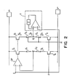
- a matching current source is comprised of two dummy switches (S1, S2), two current switches (S3, S4), four current mirror transistors (T5, T6, T7 and T8) and an operational amplifier OP.
- the transistor T5, switches S1 and S2 and transistor T6 are connected in series in that order between the supply voltage terminals V+ and V-, and the transistor T7, switches S3 and S4 and transistor T8 are connected in series in that order between the terminals V+ and V-.
- the non-inverting input of the amplifier OP is connected to the node I between the switches S1 and S2 and the output of the amplifier is coupled to the gates of the transistors T5 and T7.
- the switches S3 and S4 are controlled by the voltage at node H.
- the voltage at node F is applied to the gates of the transistors T6 and T8.
- the node G at the junction of switches S3 and S4 is connected to the inverting input of an operational amplifier in the feedback circuit 1 and the voltage at node E is applied to the inverting input of the operational amplifier OP as well as to the non-inverting input of the operational amplifier in the feedback circuit 1.
- the feedback circuit may be comprised of the above discussed operational amplifier having a feedback impedance Z, the output terminal J of the feedback circuit having a voltage waveform that is symmetrical in both the sourcing and sinking modes with respect to the voltage V(E) applied to the node E.
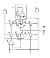
- FIG. 3 in accordance with a first preferred embodiment of the invention.
- This circuit differs from that of Fig. 2 only in that S1, S2, S3 and S4 are all MOS transistors.
- the gate of the transistor employed for the switch S1 is illustrated as connected to the terminal V- and the gate of the transistor employed for the switch S2 is illustrated as connected to the terminal V+, whereby both of the transistors are always conductive.
- the feedback circuit 1 of Fig. 3 is replaced by integrator 2 as shown.
- the integrator as illustrated may be comprised of an operational amplifier with a feedback capacitor C1.
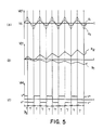
- V(H) of Fig. 5(c) is voltage waveform applied to node H of Fig. 4, initially the voltage across the capacitor C1 is zero. If node F is set at a constant voltage, the voltage waveform of the output J of the integrator is the waveform a1 of Fig. 5(a). If node F is set at a different constant voltage, the waveform will change to the waveform a2 of Fig. 5(a).
Abstract
Description
- This invention relates to current sources and is more in particular directed to a matching current source for providing the same quantity of sink current as source current.
- In many integrated circuits, particularly analog circuits, current sources are frequently used. For some cases, a matching current source which generates equivalent sink and source current is very important. However, it is recognized that the transistor current is affected by the channel length modulation effect in MOS devices and Early Effect in bipolar devices. The drain currents of MOS transistors are consequently not independent of their drain-source voltages and the collector currents of bipolar transistors are not independent of their collector-emitter voltages. Actually, the drain current (collector current) increases with increasing drain-source voltage (collector-emitter voltage).
- Fig. 1 illustrates the circuit of a known current source which provides sink current and source current. In this circuit, MOS transistors T1 and T2 are serially connected, with the sources of the transistors T1 and T2 being connected to the voltage terminals V+ and V- respectively and the gate of transistors T1 being connected to its drain at node F. Node F is also coupled to the gate of transistor T3 having its source connected to the terminal V+. Input voltages at node B are applied to the gate of transistor T2 as well as to the gate of a transistor T4 that has its source connected to the voltage terminal V-. A voltage node A controls a switch S, for selectively connecting output node C to the drains of the transistors T3 and T4, at terminals D and E respectively.
- Since the channel length modulation effect exists, this circuit can't provide equivalent sink and source current. Node B controls the amplitude of source current. Node C is an output node which is at a fixed voltage in the range between V+ and V-. When node A controls the switch S to close the contact between C and D and open the contact between C and E, this circuit functions to source current. Changes in the voltage applied to node B change the current I1. The drain-source voltage Vds1 of transistor T1 and drain-source voltage Vds2 of transistor T2 vary in opposite directions with changes in the voltage of node B. However, the voltage of node C is constant. Therefore, Vds1-Vds2, Vds1-Vds3 and Vds2-Vds4 vary with changes in the voltage of node B. Vds1, Vds2, Vds2 and Vds4 are the drain-source voltages of transistors T1, T2, T3 and T4 respectively. Not only transistors T1 and T2, but also transistors T2 and T4, experience the different degree of channel length modulation effect. A linear relationship consequently does not exist between currents I1 and I2, and a linear relationship does not exist between currents I3 and I1. Similarly a linear relation does not exist between currents I2 and I3. Moreover, the ratios of current I4(-I2) in the sourcing current mode and the current -I4(=I3) in the sinking current mode are different for different voltages at node B. Therefore, this circuit can't provide matched current. In a matched current condition the amplitude of source current in a sourcing current mode is the same as the amplitude of sink current in sinking current mode, independently of whether those currents are large or small.
- One method commonly employed to overcome this problem is the adjustment of the current source by laser trimming. However, this method only provides equivalent source and sink current at one constant current, and the ratio of source-to-sink current varies with different amplitudes of source and sink current.
- A matching current source may be implemented by MOS transistors or bipolar transistors. In spite of the effects of the channel length modulation effect or the Early Effect, the circuit of the invention provides equivalent sink and source current independently of whether the output currents are large or small.
- Briefly stated, in accordance with the invention, a matching current source comprises a first stage of a series connected first transistor, a pair of constantly on switches and a second transistor in that order, and a second stage of a series connected third transistor, a pair of current switches, and a fourth transistor in that order. An operational amplifier has a noninverting input coupled to the junction of the constantly on switches, and an output coupled to control the first and third transistors. The third and fourth switches are connected to control the sourcing or sinking mode of operation, and their junction in held at substantially the same potential as the inverting input of the operational amplifier.
- An output feedback circuit or integrator may be coupled to the junction of third and fourth switches.
-
- Fig. 1 is a circuit diagram of a prior art current source;
- Fig. 2 is a simplified schematic diagram of the current source of the present invention;
- Fig. 3 is a circuit diagram of one embodiment of the present invention;
- Fig. 4 is a circuit diagram of another embodiment of the present invention; and
- Fig. 5 is the comparison of waveforms of the matching current source of the present invention and prior current source, assuming the connection of the outputs of these circuits to the same integrator.
- A schematic diagram of matching current source of the present invention is illustrated in Fig. 2. As illustrated in this figure, a matching current source is comprised of two dummy switches (S1, S2), two current switches (S3, S4), four current mirror transistors (T5, T6, T7 and T8) and an operational amplifier OP.
- As illustrated in Fig. 2, The transistor T5, switches S1 and S2 and transistor T6 are connected in series in that order between the supply voltage terminals V+ and V-, and the transistor T7, switches S3 and S4 and transistor T8 are connected in series in that order between the terminals V+ and V-. The non-inverting input of the amplifier OP is connected to the node I between the switches S1 and S2 and the output of the amplifier is coupled to the gates of the transistors T5 and T7. The switches S3 and S4 are controlled by the voltage at node H. The voltage at node F is applied to the gates of the transistors T6 and T8. The node G, at the junction of switches S3 and S4 is connected to the inverting input of an operational amplifier in the feedback circuit 1 and the voltage at node E is applied to the inverting input of the operational amplifier OP as well as to the non-inverting input of the operational amplifier in the feedback circuit 1. As illustrated in Fig. 2, the feedback circuit may be comprised of the above discussed operational amplifier having a feedback impedance Z, the output terminal J of the feedback circuit having a voltage waveform that is symmetrical in both the sourcing and sinking modes with respect to the voltage V(E) applied to the node E.
- Current switches S3 and S4, which are controlled by node H, must have one of the two following conditions:
- (i) S3 is on (conductive) and S4 is off (nonconductive) when the matching current source operates in the sourcing current mode.
- (ii) S3 is off and S4 is on when the matching current source operates in the sinking current mode.
- (i) I8=I6=X*I5 is true since Vgs5=Vgs7, Vds5=Vds7 and (W/L) of T7 = X*(W/L) of T5 when S3 is on and S4 is off.
- (ii) -I8=I7=X*I5 is true since Vgs6=Vgs8, Vds6=Vds8 and (W/L) of T8 = X*(W/L) of T6 when S3 is off and S4 is on.
- If, in a modification of the circuit shown in Fig. 2, the transistors T5, T6, T7 and T8 are bipolar transistors and the condition:

- Referring to Fig. 3, in accordance with a first preferred embodiment of the invention. This circuit differs from that of Fig. 2 only in that S1, S2, S3 and S4 are all MOS transistors. The gate of the transistor employed for the switch S1 is illustrated as connected to the terminal V- and the gate of the transistor employed for the switch S2 is illustrated as connected to the terminal V+, whereby both of the transistors are always conductive. In this circuit:

- Referring to Fig. 4, in accordance with another preferred embodiment of the invention, the feedback circuit 1 of Fig. 3 is replaced by
integrator 2 as shown. In this circuit, the integrator as illustrated may be comprised of an operational amplifier with a feedback capacitor C1. - Assuming V(H) of Fig. 5(c) is voltage waveform applied to node H of Fig. 4, initially the voltage across the capacitor C1 is zero. If node F is set at a constant voltage, the voltage waveform of the output J of the integrator is the waveform a1 of Fig. 5(a). If node F is set at a different constant voltage, the waveform will change to the waveform a2 of Fig. 5(a). The waveform a1 and a2 both are symmetrical waveforms with respect to V(E), the voltage of node E , since the voltage slope of integrator output dV(J)/dt equals I7/C1 when V(H)=V+ and the voltage slope of integrator output dV(J)/dt equals-I6/C1 when V(H)=V-. If the matching current source of the invention were replaced by the current source in Fig. 1, waveforms a1 and a2 of Fig 5(a) would be expected to change to the waveform b1 and b2 as shown in Fig. 5(b). The waveforms b1 and b2 are not symmetrical to any constant voltage.
- While the invention has been disclosed and described with reference to a limited number of embodiments, it will be apparent that many variations and modifications may be made therein, and it is therefore intended in the following claims to cover each such variation and modification as falls within the true spirit and scope of the invention.

Claims (12)
a first circuit stage comprising a first transistor, a set of dummy switches comprising first and second constantly on switches, and a second transistor, connected in series in that order;
a second circuit stage comprising a third transistor, a set of current switches comprising third and fourth switches, and a fourth transistor, connected in series in that order;
means for selectively setting said third and fourth switches to have a first state with the third switch on and the fourth switch off, and a second state with the third switch off and the fourth switch on;
an operational amplifier having its output coupled to the input electrodes of the first and third transistors;
the noninverting input of the operational amplifier being coupled to the junction between the first and second switches and its inverting input being connected to have the same voltage as the junction point between third and fourth switch;
whereby, depending on the first or second states of said third and fourth switch, the matching current source provides a current sink or source.
Priority Applications (1)
| Application Number | Priority Date | Filing Date | Title |
|---|---|---|---|
| AT87303187T ATE77498T1 (en) | 1986-11-20 | 1987-04-13 | ADAPTED POWER SOURCE. |
Applications Claiming Priority (2)
| Application Number | Priority Date | Filing Date | Title |
|---|---|---|---|
| US932933 | 1986-11-20 | ||
| US06/932,933 US4706013A (en) | 1986-11-20 | 1986-11-20 | Matching current source |
Publications (3)
| Publication Number | Publication Date |
|---|---|
| EP0268345A2 true EP0268345A2 (en) | 1988-05-25 |
| EP0268345A3 EP0268345A3 (en) | 1988-10-12 |
| EP0268345B1 EP0268345B1 (en) | 1992-06-17 |
Family
ID=25463172
Family Applications (1)
| Application Number | Title | Priority Date | Filing Date |
|---|---|---|---|
| EP87303187A Expired - Lifetime EP0268345B1 (en) | 1986-11-20 | 1987-04-13 | Matching current source |
Country Status (5)
| Country | Link |
|---|---|
| US (1) | US4706013A (en) |
| EP (1) | EP0268345B1 (en) |
| JP (1) | JPH0654455B2 (en) |
| AT (1) | ATE77498T1 (en) |
| DE (1) | DE3779871T2 (en) |
Cited By (3)
| Publication number | Priority date | Publication date | Assignee | Title |
|---|---|---|---|---|
| EP0373471A1 (en) * | 1988-12-16 | 1990-06-20 | STMicroelectronics S.r.l. | Current source circuit with complementary current mirrors |
| US5717623A (en) * | 1995-08-31 | 1998-02-10 | U.S. Philips Corporation | Analog current memory having resistance to reduce current transport error |
| EP1310852A2 (en) * | 2001-09-13 | 2003-05-14 | Infineon Technologies AG | System with a current source and associated serial switch |
Families Citing this family (11)
| Publication number | Priority date | Publication date | Assignee | Title |
|---|---|---|---|---|
| US4904922B1 (en) * | 1985-03-21 | 1992-09-01 | Apparatus for converting between digital and analog values | |
| GB2201535B (en) * | 1987-02-25 | 1990-11-28 | Motorola Inc | Cmos analog multiplying circuit |
| US5266887A (en) * | 1988-05-24 | 1993-11-30 | Dallas Semiconductor Corp. | Bidirectional voltage to current converter |
| US5525897A (en) * | 1988-05-24 | 1996-06-11 | Dallas Semiconductor Corporation | Transistor circuit for use in a voltage to current converter circuit |
| DE4034371C1 (en) * | 1990-10-29 | 1991-10-31 | Eurosil Electronic Gmbh, 8057 Eching, De | |
| IT1246598B (en) * | 1991-04-12 | 1994-11-24 | Sgs Thomson Microelectronics | BAND-GAP CHAMPIONSHIP VOLTAGE REFERENCE CIRCUIT |
| US5153499A (en) * | 1991-09-18 | 1992-10-06 | Allied-Signal Inc. | Precision voltage controlled current source with variable compliance |
| US5453680A (en) * | 1994-01-28 | 1995-09-26 | Texas Instruments Incorporated | Charge pump circuit and method |
| DE69739232D1 (en) * | 1997-10-15 | 2009-03-12 | Em Microelectronic Marin Sa | Process for producing a very precise current |
| JP3262103B2 (en) * | 1999-06-07 | 2002-03-04 | 日本電気株式会社 | Semiconductor device having internal power supply circuit |
| US6566851B1 (en) | 2000-08-10 | 2003-05-20 | Applied Micro Circuits, Corporation | Output conductance correction circuit for high compliance short-channel MOS switched current mirror |
Citations (5)
| Publication number | Priority date | Publication date | Assignee | Title |
|---|---|---|---|---|
| US3683270A (en) * | 1971-02-22 | 1972-08-08 | Signetics Corp | Integrated circuit bilateral current source |
| US4283673A (en) * | 1979-12-19 | 1981-08-11 | Signetics Corporation | Means for reducing current-gain modulation due to differences in collector-base voltages on a transistor pair |
| EP0121793A1 (en) * | 1983-03-14 | 1984-10-17 | Vitatron Medical B.V. | CMOS circuits with parameter adapted voltage regulator |
| EP0169388A1 (en) * | 1984-07-16 | 1986-01-29 | Siemens Aktiengesellschaft | Integrated constant-current source |
| US4642551A (en) * | 1985-10-22 | 1987-02-10 | Motorola, Inc. | Current to voltage converter circuit |
Family Cites Families (2)
| Publication number | Priority date | Publication date | Assignee | Title |
|---|---|---|---|---|
| NL7700807A (en) * | 1977-01-27 | 1978-07-31 | Philips Nv | POWER STABILIZER. |
| US4186437A (en) * | 1978-05-03 | 1980-01-29 | California Institute Of Technology | Push-pull switching power amplifier |
-
1986
- 1986-11-20 US US06/932,933 patent/US4706013A/en not_active Expired - Lifetime
-
1987
- 1987-04-13 EP EP87303187A patent/EP0268345B1/en not_active Expired - Lifetime
- 1987-04-13 AT AT87303187T patent/ATE77498T1/en not_active IP Right Cessation
- 1987-04-13 DE DE8787303187T patent/DE3779871T2/en not_active Expired - Fee Related
- 1987-07-13 JP JP62174574A patent/JPH0654455B2/en not_active Expired - Lifetime
Patent Citations (5)
| Publication number | Priority date | Publication date | Assignee | Title |
|---|---|---|---|---|
| US3683270A (en) * | 1971-02-22 | 1972-08-08 | Signetics Corp | Integrated circuit bilateral current source |
| US4283673A (en) * | 1979-12-19 | 1981-08-11 | Signetics Corporation | Means for reducing current-gain modulation due to differences in collector-base voltages on a transistor pair |
| EP0121793A1 (en) * | 1983-03-14 | 1984-10-17 | Vitatron Medical B.V. | CMOS circuits with parameter adapted voltage regulator |
| EP0169388A1 (en) * | 1984-07-16 | 1986-01-29 | Siemens Aktiengesellschaft | Integrated constant-current source |
| US4642551A (en) * | 1985-10-22 | 1987-02-10 | Motorola, Inc. | Current to voltage converter circuit |
Cited By (4)
| Publication number | Priority date | Publication date | Assignee | Title |
|---|---|---|---|---|
| EP0373471A1 (en) * | 1988-12-16 | 1990-06-20 | STMicroelectronics S.r.l. | Current source circuit with complementary current mirrors |
| US5717623A (en) * | 1995-08-31 | 1998-02-10 | U.S. Philips Corporation | Analog current memory having resistance to reduce current transport error |
| EP1310852A2 (en) * | 2001-09-13 | 2003-05-14 | Infineon Technologies AG | System with a current source and associated serial switch |
| EP1310852A3 (en) * | 2001-09-13 | 2004-10-13 | Infineon Technologies AG | System with a current source and associated serial switch |
Also Published As
| Publication number | Publication date |
|---|---|
| EP0268345B1 (en) | 1992-06-17 |
| ATE77498T1 (en) | 1992-07-15 |
| DE3779871T2 (en) | 1993-02-04 |
| US4706013A (en) | 1987-11-10 |
| DE3779871D1 (en) | 1992-07-23 |
| JPS63138411A (en) | 1988-06-10 |
| EP0268345A3 (en) | 1988-10-12 |
| JPH0654455B2 (en) | 1994-07-20 |
Similar Documents
| Publication | Publication Date | Title |
|---|---|---|
| US4274014A (en) | Switched current source for current limiting complementary symmetry inverter | |
| US6384684B1 (en) | Amplifier | |
| US4379267A (en) | Low power differential amplifier | |
| EP0045841B1 (en) | Linear voltage-current converter | |
| EP0268345B1 (en) | Matching current source | |
| KR920020847A (en) | Sample Band-Gap Voltage Reference Circuit | |
| US20020089351A1 (en) | Integrated circuit and method of controlling output impedance | |
| US5285148A (en) | Current-regulating circuit having parallel control paths | |
| US4961046A (en) | Voltage-to-current converter | |
| KR100209098B1 (en) | D/a converter | |
| KR950000432B1 (en) | Simulated transistor/diode | |
| KR920010237B1 (en) | Amplifier | |
| US5635868A (en) | Power transistor current limiter | |
| US6429685B1 (en) | Integrated circuit and method of controlling output impedance | |
| EP0157447B1 (en) | Differential amplifier | |
| KR860000906B1 (en) | Sample circuit | |
| US4333025A (en) | N-Channel MOS comparator | |
| US4847566A (en) | CMOS Amplifier having enhanced current sinking and capacitance load drive | |
| US6700362B2 (en) | Switchable current source | |
| JPH02177724A (en) | Output buffer circuit | |
| JP2896029B2 (en) | Voltage-current converter | |
| US6507242B1 (en) | Gain switching scheme for amplifiers with digital automatic gain control | |
| JPH084168B2 (en) | Optical semiconductor element drive circuit | |
| JP2748478B2 (en) | Constant voltage generator | |
| KR0154302B1 (en) | Voltage-current converter |
Legal Events
| Date | Code | Title | Description |
|---|---|---|---|
| PUAI | Public reference made under article 153(3) epc to a published international application that has entered the european phase |
Free format text: ORIGINAL CODE: 0009012 |
|
| AK | Designated contracting states |
Kind code of ref document: A2 Designated state(s): AT BE CH DE ES FR GB GR IT LI LU NL SE |
|
| PUAL | Search report despatched |
Free format text: ORIGINAL CODE: 0009013 |
|
| AK | Designated contracting states |
Kind code of ref document: A3 Designated state(s): AT BE CH DE ES FR GB GR IT LI LU NL SE |
|
| 17P | Request for examination filed |
Effective date: 19890118 |
|
| 17Q | First examination report despatched |
Effective date: 19901106 |
|
| GRAA | (expected) grant |
Free format text: ORIGINAL CODE: 0009210 |
|
| AK | Designated contracting states |
Kind code of ref document: B1 Designated state(s): AT BE CH DE ES FR GB GR IT LI LU NL SE |
|
| PG25 | Lapsed in a contracting state [announced via postgrant information from national office to epo] |
Ref country code: SE Effective date: 19920617 Ref country code: GR Free format text: LAPSE BECAUSE OF FAILURE TO SUBMIT A TRANSLATION OF THE DESCRIPTION OR TO PAY THE FEE WITHIN THE PRESCRIBED TIME-LIMIT Effective date: 19920617 Ref country code: AT Effective date: 19920617 |
|
| REF | Corresponds to: |
Ref document number: 77498 Country of ref document: AT Date of ref document: 19920715 Kind code of ref document: T |
|
| REF | Corresponds to: |
Ref document number: 3779871 Country of ref document: DE Date of ref document: 19920723 |
|
| ITF | It: translation for a ep patent filed |
Owner name: STUDIO TORTA SOCIETA' SEMPLICE |
|
| PG25 | Lapsed in a contracting state [announced via postgrant information from national office to epo] |
Ref country code: ES Free format text: LAPSE BECAUSE OF FAILURE TO SUBMIT A TRANSLATION OF THE DESCRIPTION OR TO PAY THE FEE WITHIN THE PRESCRIBED TIME-LIMIT Effective date: 19920928 |
|
| ET | Fr: translation filed | ||
| PLBE | No opposition filed within time limit |
Free format text: ORIGINAL CODE: 0009261 |
|
| STAA | Information on the status of an ep patent application or granted ep patent |
Free format text: STATUS: NO OPPOSITION FILED WITHIN TIME LIMIT |
|
| ITTA | It: last paid annual fee | ||
| PG25 | Lapsed in a contracting state [announced via postgrant information from national office to epo] |
Ref country code: LU Free format text: LAPSE BECAUSE OF NON-PAYMENT OF DUE FEES Effective date: 19930430 |
|
| 26N | No opposition filed | ||
| PGFP | Annual fee paid to national office [announced via postgrant information from national office to epo] |
Ref country code: CH Payment date: 19950313 Year of fee payment: 9 |
|
| PG25 | Lapsed in a contracting state [announced via postgrant information from national office to epo] |
Ref country code: LI Effective date: 19960430 Ref country code: CH Effective date: 19960430 |
|
| REG | Reference to a national code |
Ref country code: CH Ref legal event code: PL |
|
| PGFP | Annual fee paid to national office [announced via postgrant information from national office to epo] |
Ref country code: DE Payment date: 20000410 Year of fee payment: 14 |
|
| PGFP | Annual fee paid to national office [announced via postgrant information from national office to epo] |
Ref country code: FR Payment date: 20000411 Year of fee payment: 14 |
|
| PGFP | Annual fee paid to national office [announced via postgrant information from national office to epo] |
Ref country code: GB Payment date: 20000412 Year of fee payment: 14 |
|
| PGFP | Annual fee paid to national office [announced via postgrant information from national office to epo] |
Ref country code: NL Payment date: 20000428 Year of fee payment: 14 |
|
| PGFP | Annual fee paid to national office [announced via postgrant information from national office to epo] |
Ref country code: BE Payment date: 20000622 Year of fee payment: 14 |
|
| PG25 | Lapsed in a contracting state [announced via postgrant information from national office to epo] |
Ref country code: GB Free format text: LAPSE BECAUSE OF NON-PAYMENT OF DUE FEES Effective date: 20010413 |
|
| PG25 | Lapsed in a contracting state [announced via postgrant information from national office to epo] |
Ref country code: FR Free format text: THE PATENT HAS BEEN ANNULLED BY A DECISION OF A NATIONAL AUTHORITY Effective date: 20010430 Ref country code: BE Free format text: LAPSE BECAUSE OF NON-PAYMENT OF DUE FEES Effective date: 20010430 |
|
| BERE | Be: lapsed |
Owner name: INDUSTRIAL TECHNOLOGY RESEARCH INSTITUTE Effective date: 20010430 |
|
| PG25 | Lapsed in a contracting state [announced via postgrant information from national office to epo] |
Ref country code: NL Free format text: LAPSE BECAUSE OF NON-PAYMENT OF DUE FEES Effective date: 20011101 |
|
| GBPC | Gb: european patent ceased through non-payment of renewal fee |
Effective date: 20010413 |
|
| NLV4 | Nl: lapsed or anulled due to non-payment of the annual fee |
Effective date: 20011101 |
|
| PG25 | Lapsed in a contracting state [announced via postgrant information from national office to epo] |
Ref country code: DE Free format text: LAPSE BECAUSE OF NON-PAYMENT OF DUE FEES Effective date: 20020201 |
|
| REG | Reference to a national code |
Ref country code: FR Ref legal event code: ST |
|
| PG25 | Lapsed in a contracting state [announced via postgrant information from national office to epo] |
Ref country code: IT Free format text: LAPSE BECAUSE OF NON-PAYMENT OF DUE FEES;WARNING: LAPSES OF ITALIAN PATENTS WITH EFFECTIVE DATE BEFORE 2007 MAY HAVE OCCURRED AT ANY TIME BEFORE 2007. THE CORRECT EFFECTIVE DATE MAY BE DIFFERENT FROM THE ONE RECORDED. Effective date: 20050413 |