EP0267587A2 - Halbleiterspeichergerät mit Zellanordnung - Google Patents
Halbleiterspeichergerät mit Zellanordnung Download PDFInfo
- Publication number
- EP0267587A2 EP0267587A2 EP87116603A EP87116603A EP0267587A2 EP 0267587 A2 EP0267587 A2 EP 0267587A2 EP 87116603 A EP87116603 A EP 87116603A EP 87116603 A EP87116603 A EP 87116603A EP 0267587 A2 EP0267587 A2 EP 0267587A2
- Authority
- EP
- European Patent Office
- Prior art keywords
- memory cell
- memory
- memory device
- block
- blocks
- Prior art date
- Legal status (The legal status is an assumption and is not a legal conclusion. Google has not performed a legal analysis and makes no representation as to the accuracy of the status listed.)
- Withdrawn
Links
- 239000004065 semiconductor Substances 0.000 title claims abstract description 10
- 230000015654 memory Effects 0.000 claims abstract description 100
- 238000012360 testing method Methods 0.000 claims abstract description 50
- 239000003990 capacitor Substances 0.000 claims description 10
- 230000004044 response Effects 0.000 claims description 6
- 230000005669 field effect Effects 0.000 claims 1
- 238000010586 diagram Methods 0.000 description 5
- 230000006399 behavior Effects 0.000 description 4
- 230000008859 change Effects 0.000 description 4
- 230000008878 coupling Effects 0.000 description 4
- 238000010168 coupling process Methods 0.000 description 4
- 238000005859 coupling reaction Methods 0.000 description 4
- 230000000694 effects Effects 0.000 description 4
- 229910021420 polycrystalline silicon Inorganic materials 0.000 description 3
- 230000006870 function Effects 0.000 description 2
- 238000003491 array Methods 0.000 description 1
- 230000000295 complement effect Effects 0.000 description 1
- 101150047356 dec-1 gene Proteins 0.000 description 1
- 238000011161 development Methods 0.000 description 1
- 230000018109 developmental process Effects 0.000 description 1
- 239000000758 substrate Substances 0.000 description 1
Images



Classifications
-
- G—PHYSICS
- G11—INFORMATION STORAGE
- G11C—STATIC STORES
- G11C29/00—Checking stores for correct operation ; Subsequent repair; Testing stores during standby or offline operation
- G11C29/04—Detection or location of defective memory elements, e.g. cell constructio details, timing of test signals
- G11C29/08—Functional testing, e.g. testing during refresh, power-on self testing [POST] or distributed testing
- G11C29/12—Built-in arrangements for testing, e.g. built-in self testing [BIST] or interconnection details
- G11C29/18—Address generation devices; Devices for accessing memories, e.g. details of addressing circuits
- G11C29/26—Accessing multiple arrays
Definitions
- the present invention relates to a semiconductor memory device formed on a semiconductor substrate, and more particularly to a dynamic type semiconductor device having a test circuit.
- test time for testing such large capacity of memories has been also increased.
- the test time for a 1 Mega-bit memory is four times the test time for 256 K-bit memory for the simplest case.
- the test circuit writes the same data to a plurality of memory locations, i.e. memory cells simultaneously and thereafter reads data stored in the plurality of memory locations simultaneously in a test mode.
- a test time for the test of simple read-write test for the respective memory locations is effectively reduced.
- the test circuit in performing read-write test for the memory of 1 Mega words x 1 bit structure, writes the same data to four memory locations and reads data stored in the four memory locations simultaneously so that the above memory is treated as a memory of 256 K-words x 4 bits structure.
- the above testing scheme is advantageous in reducing the test time.
- the above test by the test circuit does not evaluate the function of the memory accurately because the same data is written into a plurality of memory locations in parallel in the above test while the data is written into only one memory location in a normal operation mode. Namely, a plurality of memory locations show the same behaviour in the test mode and such behaviour mutually affects from each other among the memory locations subjected to the test through stray coupling. Therefore, operational margins in the respective memory locations obtained through the above test seems better than the practical operational margin in the normal operational mode.
- the semiconductor memory device comprises a plurality of memory cell blocks each having a plurality of memory cells, a plurality of selection circuits each provided for each of the memory cell blocks and operatively selecting only one memory cell in the associated memory cell block, a data input circuit for operatively generating a write data in response to an input data signal and a control circuit coupled between the data input circuit and the plurality of selection circuits for establish a signal path between one of the selection circuits and the data input circuit in a normal operation mode and establishing signal paths between the data input circuit and a plurality of the selection circuits in a test mode.
- a plurality of memory cells are not selected for access in each memory cell block in the test mode, but only one memory cell is selected in each memory cell block. Therefore, condition of accessing the memory cell in the test mode in the respective memory cell blocks is substantially the same as that in the selected memory cell block in the normal operation mode.
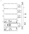
- FIG. 1 a major part of a semiconductor memory device according to a prior art will be explained.
- a plurality of one-transistor type memory cells are divided into two memory cell blocks 1 and 2.
- a plurality of word lines WL1 are arranged in rows and a plurality pairs of bit lines D11, D11; D12, D12 ... are arranged in columns.
- Memory cells such as MC11 and MC12 are arranged for the respective intersections of the word lines and bit line pairs in a known way and each of the memory cells includes a memory cell transistor Q M and a storage capacitor C M .
- One plates connected to a potential Vp which may be a power voltage Vcc, 1/2 Vcc or a ground potential, of the storage capacitors C M in the block 1 are formed of a polycrystalline silicon commonly to form a common memory cell plate.
- a row decoder (X DEC 1) 4 is used to select one of the word lines WL1 in the block 1 and a plurality of sense amplifiers SA11, SA12 enabled by a signal SE1 ... are provided for the respective bit lines pairs, D11, D1 1 ; D12, D12 ....
- word lines WL2 a plurality pairs of bit lines D21, D21; D22, D22 ... and a plurality of memory cells MC21, MC22 ... are arranged in the same way as the block 1.
- One plates connected to Vp of the storage capacitors C M in the block 1 are commonly formed of a polycrystalline silicon to form another common memory cell plate.
- a row decoder (X DEC 2) 5 is used to drive one of the word lines WL2 in the block 2 and a plurality of sense amplifiers SA21, SA22 ... amplify signal differences in the respective bit line pairs in response to an active level of a control signal SE2, in a known way.
- bus lines I/O 0 and I/0 1 Two pairs of bus lines I/O 0 and I/0 1 are provided for the block 1 and each odd number of bit line pair such as D11 and D11 are connected to the bus line pair I/O 0 via column selection transistors Qo and Q 1 which are controlled by an output of one of a column decoder (Y DEC) 6 and each even number of bit line pair, such as D12 and D12 are connected to the bus line pair I/O 1 through a pair of column selection transistors Q 2 and Q 3 .
- Y DEC column decoder
- bit line pair D21, D21 in the block 2 are connected to a bus line pair I/O 3 via column selection transistors Q 6 and Q 7 while the even number of bit line pair D22, D22 are connected to a bus line pair I/0 2 via a pair of column selection transistors 0 4 and Q 5 .
- two pairs of bit lines in the block 1. and two pairs of bit lines in the block 2 are selectively connected to the bus line pairs I/O 0, I/0 1 and I/O 2, I/O 3 respectively.
- Data amplifiers DA1 - DA4 are provided for the bus line pair I/O 0 - 1/0 3 respectively, but the amplifiers DA1 - DA4 are not essential in memory operation, and may be deleted.
- the circuit 3 determines the states of the bus line pairs I/O 0 - I/O 3 simultaneously based on the state of the input terminal D in and the same data applied to the input terminal D in are generated on the four bus line pairs I/O 0 - I/O 3 and then written into two memory cells in the block 1 via two pairs of column selection transistors and into two memory cells in the block 2 via two pairs of column selection transistors at one time in the write state.
- writing time of data to the memory cells in the blocks 1 and 2 is effectively shortened to one quarter as compared to writing in the normal operation mode.
- the condition of writing data to one memory cell such as MC11 in the block 1 in the normal operation mode is completely different from the condition of writing the same data to two memory cells such as MC11 and MC12 in the test mode.
- the normal operation mode only one pair of bit lines are subjected to change in potential with other bit lines unchanged in the respective blocks, and therefore, a change in potentials at the above one pair of bit lines are relatively suppressed through capacitive couplings among bit lines in the respective blocks.
- the test mode two pairs of bit lines are subjected to the same change in potentials and therefore the potential changes in the respective above bit lines are relatively large.
- the odd number of bit line pairs (D11, D11) and the even number of bit line pairs (D12, D12) in the block 1 in Fig. 1 are arranged in different memory blocks 1-1 and 1-2, respectively.
- the odd and even number of bit line pairs D21, D21, D22, D22 in the block 1 in Fig. 1 are arranged in different two blocks 2-1 and 2-2.
- two column decoders (Y DEC A, Y DEC B) 6-1 and 6-2 are provided for selecting the bit line pairs in the blocks 1-1 and 1-2, and 2-1 and 2-2, respectively.
- the four bit line pairs which are selected simultaneously in the test mode are located in different four memory blocks 1-1 to 2-2, respectively.
- the blocks 1-1, 1-2, 2-1 and 2-2 only one pair of bit lines are subjected to writing of data thereto in the test mode. This condition in the test mode is very similar or equal to that in the normal operation mode.
- the memory cells are of one transistor type composed of the transistor Q M and the storage capacitor C M as shown in Fig. 1 and the capacitor plates connected to Vp of the capacitors C M are commonly formed of a single plate of polycrystalline silicon in each of blocks 1-1 to 2-2.
- I/O select circuit 3 One example of the I/O select circuit 3 is shown in Fig. 3.
- the select circuit 3 includes a pair of data bus lines DB and DB, and four pairs of transfer gate transistors OY 11 , QY 12 ; QY 21 , QY 22 ; QY 31 , QY 32 ; QY 41 , QY 42 coupted between the data bus lines DB and
- the data bus lines DB and DB are connected to a pair of output of an input buffer 11 and a pair of input of an output buffer 12.
- the output buffer 12 is enabled in a read state in which the control signal R/W is high while the input buffer 11 is enabled in a write state in which the signal R/W is low in level and its inverted signal R/W by an inverter INV is high in level.
- An address inverter 13 receives two bits of address signals AO and A1 and generates their true and complementary signals AO', AO , A1' and A1 in a known way.
- Each of four NOR gates NG1 - NG4 receives two of the four outputs of the inverters 13 in a predetermined combination to achieve a decoder function for selecting one pair of transfer gate transistors.
- Clamp transistors QTo -QT 3 are coupled between the respective outputs AO', A1', AO and A1 and the ground potential.
- the test signal TE is at a low inactive level and the transistors QT o -QT 3 are non-conductive. Therefore, according to the contents of the address signals AO and A1, one (e.g. NG1) of the NOR gates NG1 - NG4 is made active and its corresponding pair of transfer gate transistors (e.g. QY 11 , QY 12 ) are made conductive.
- FIG. 4 a memory device according to another embodiment of the present invention is explained.
- the memory device includes two memory arrays 20A and 20B each of which is basically the same as the memory of Fig. 1 except that a bus line selectors 21 and 22 are provided.
- the bus line selector 21 selectively connects one of two bus line pairs 1/0 0 and 1/0 1 to the amplifier DA1 in response, to content of an address signal A3.
- the bus line selecter 22 similarly selects one of two bus line pairs 1/0 2 and 1/0 3 for connection to the amplifier DA2 in response to A3. Therefore, the unit of column decoder 6 first selects two bit line pairs in the block 1 and two bit line pairs in the block 2 and the selecter 21 selects one bit line pair in the block 1 finally and the selecter 22 also selects one bit line pair in the block 2.
- the array 20B has the same structure as the array 20A. Thus, in the test mode, only one pair of bit lines are selected in each of memory blocks, and the same effect and advantages can be achieved in this embodiment as those in the previous embodiment.
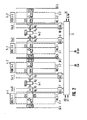
- a memory device Referring to Fig. 5, a memory device according to a third embodiment.
- This embodiment is electrically the same as that of Fig. 2, but is different in the arrangement of memory cells.
- the memory blocks 1-1', 1-2', 2-1' and 2-2' of Fig. 5 correspond to the blocks 1-1, 1-2, 2-1 and 2-2 in Fig. 2, respectively.
- the sense amplifiers e.g. SA11
- the block 1-1 in Fig. 2 is divided into two sub-blocks 11 and 12. It is apparent that the embodiment of Fig. 5 achieves the same effect as the previous embodiments.
Landscapes
- For Increasing The Reliability Of Semiconductor Memories (AREA)
- Techniques For Improving Reliability Of Storages (AREA)
- Dram (AREA)
Applications Claiming Priority (2)
| Application Number | Priority Date | Filing Date | Title |
|---|---|---|---|
| JP61268221A JPH0828115B2 (ja) | 1986-11-10 | 1986-11-10 | 半導体メモリ装置 |
| JP268221/86 | 1986-11-10 |
Publications (2)
| Publication Number | Publication Date |
|---|---|
| EP0267587A2 true EP0267587A2 (de) | 1988-05-18 |
| EP0267587A3 EP0267587A3 (de) | 1990-03-28 |
Family
ID=17455593
Family Applications (1)
| Application Number | Title | Priority Date | Filing Date |
|---|---|---|---|
| EP87116603A Withdrawn EP0267587A3 (de) | 1986-11-10 | 1987-11-10 | Halbleiterspeichergerät mit Zellanordnung |
Country Status (2)
| Country | Link |
|---|---|
| EP (1) | EP0267587A3 (de) |
| JP (1) | JPH0828115B2 (de) |
Cited By (1)
| Publication number | Priority date | Publication date | Assignee | Title |
|---|---|---|---|---|
| FR2656729A1 (fr) * | 1989-12-29 | 1991-07-05 | Samsung Electronics Co Ltd | Dispositif memoire a semi-conducteurs pour la realisation d'un test d'ecriture en parallele et sa methode d'application. |
Family Cites Families (4)
| Publication number | Priority date | Publication date | Assignee | Title |
|---|---|---|---|---|
| JPS57105897A (en) * | 1980-12-23 | 1982-07-01 | Fujitsu Ltd | Semiconductor storage device |
| US4541090A (en) * | 1981-06-09 | 1985-09-10 | Matsushita Electric Industrial Co., Ltd. | Semiconductor memory device |
| JPS60115099A (ja) * | 1983-11-25 | 1985-06-21 | Fujitsu Ltd | 半導体記憶装置 |
| JPS6159698A (ja) * | 1984-08-30 | 1986-03-27 | Mitsubishi Electric Corp | 半導体記憶装置 |
-
1986
- 1986-11-10 JP JP61268221A patent/JPH0828115B2/ja not_active Expired - Lifetime
-
1987
- 1987-11-10 EP EP87116603A patent/EP0267587A3/de not_active Withdrawn
Cited By (1)
| Publication number | Priority date | Publication date | Assignee | Title |
|---|---|---|---|---|
| FR2656729A1 (fr) * | 1989-12-29 | 1991-07-05 | Samsung Electronics Co Ltd | Dispositif memoire a semi-conducteurs pour la realisation d'un test d'ecriture en parallele et sa methode d'application. |
Also Published As
| Publication number | Publication date |
|---|---|
| EP0267587A3 (de) | 1990-03-28 |
| JPH0828115B2 (ja) | 1996-03-21 |
| JPS63121198A (ja) | 1988-05-25 |
Similar Documents
| Publication | Publication Date | Title |
|---|---|---|
| US4873669A (en) | Random access memory device operable in a normal mode and in a test mode | |
| US4837747A (en) | Redundary circuit with a spare main decoder responsive to an address of a defective cell in a selected cell block | |
| US4658377A (en) | Dynamic memory array with segmented bit lines | |
| US4464750A (en) | Semiconductor memory device | |
| JP2673395B2 (ja) | 半導体記憶装置およびそのテスト方法 | |
| EP0264929B1 (de) | Halbleiterspeicheranordnung mit verbesserter Bitzeilenordnung | |
| USRE35953E (en) | Semiconductor dynamic memory device | |
| KR920009059B1 (ko) | 반도체 메모리 장치의 병렬 테스트 방법 | |
| US5335199A (en) | Multiport memory | |
| US4897817A (en) | Semiconductor memory device with a built-in test circuit | |
| US6137737A (en) | Method and circuit for rapidly equilibrating paired digit lines of a memory device during testing | |
| US4418399A (en) | Semiconductor memory system | |
| US6215721B1 (en) | Multi-bank memory device and method for arranging input/output lines | |
| US6788600B2 (en) | Non-volatile semiconductor memory | |
| US4630240A (en) | Dynamic memory with intermediate column derode | |
| EP0456195A2 (de) | Direktzugriffsspeicher mit Hilfsredundanzschaltung | |
| US5828622A (en) | Clocked sense amplifier with wordline tracking | |
| US4701885A (en) | Dynamic memory array with quasi-folded bit lines | |
| EP0953912B1 (de) | Halbleiterspeicheranordnung mit Redundanz | |
| US4878201A (en) | Semiconductor memory device having an improved timing signal generator for the column selection circuit | |
| KR100351048B1 (ko) | 데이터 입출력 라인의 부하를 최소화하는 칼럼 선택 회로, 이를 구비하는 반도체 메모리 장치 | |
| USRE33694E (en) | Dynamic memory array with segmented bit lines | |
| JPH0821239B2 (ja) | ダイナミック型半導体記憶装置およびそのテスト方法 | |
| US6330198B1 (en) | Semiconductor storage device | |
| JP3283547B2 (ja) | 半導体メモリ装置 |
Legal Events
| Date | Code | Title | Description |
|---|---|---|---|
| PUAI | Public reference made under article 153(3) epc to a published international application that has entered the european phase |
Free format text: ORIGINAL CODE: 0009012 |
|
| 17P | Request for examination filed |
Effective date: 19871110 |
|
| AK | Designated contracting states |
Kind code of ref document: A2 Designated state(s): DE FR GB |
|
| PUAL | Search report despatched |
Free format text: ORIGINAL CODE: 0009013 |
|
| AK | Designated contracting states |
Kind code of ref document: A3 Designated state(s): DE FR GB |
|
| 17Q | First examination report despatched |
Effective date: 19910708 |
|
| STAA | Information on the status of an ep patent application or granted ep patent |
Free format text: STATUS: THE APPLICATION HAS BEEN WITHDRAWN |
|
| 18W | Application withdrawn |
Withdrawal date: 19920108 |
|
| R18W | Application withdrawn (corrected) |
Effective date: 19920108 |
|
| RIN1 | Information on inventor provided before grant (corrected) |
Inventor name: FUJII, TAKEOC/O NEC CORPORATION |