EP0262013A1 - Sense amplifier - Google Patents
Sense amplifier Download PDFInfo
- Publication number
- EP0262013A1 EP0262013A1 EP87401936A EP87401936A EP0262013A1 EP 0262013 A1 EP0262013 A1 EP 0262013A1 EP 87401936 A EP87401936 A EP 87401936A EP 87401936 A EP87401936 A EP 87401936A EP 0262013 A1 EP0262013 A1 EP 0262013A1
- Authority
- EP
- European Patent Office
- Prior art keywords
- amplifier
- signal
- voltage
- transistor
- transistors
- Prior art date
- Legal status (The legal status is an assumption and is not a legal conclusion. Google has not performed a legal analysis and makes no representation as to the accuracy of the status listed.)
- Granted
Links
Images
Classifications
-
- G—PHYSICS
- G11—INFORMATION STORAGE
- G11C—STATIC STORES
- G11C7/00—Arrangements for writing information into, or reading information out from, a digital store
- G11C7/06—Sense amplifiers; Associated circuits, e.g. timing or triggering circuits
- G11C7/065—Differential amplifiers of latching type
Definitions
- the invention relates to an amplification device, commonly called a reading amplifier, used to amplify the voltage difference appearing between two lines and representing an information bit.
- Such amplifiers also serve to stabilize the voltage levels of the two bit lines.
- the bit lines can be the output lines of a memory cell delivering voltage levels requiring amplification.
- the read amplifier according to the invention can be applied to both static and dynamic memory cells.
- the bit lines can also be connected to the output lines of a logic circuit forming part of an operator belonging for example to a central processing unit of a computer.
- the amplifier according to the invention is particularly well suited for amplifying the circuit output signals produced in CMOS technology.
- the sense amplifiers must maintain the two bit lines at predetermined and stable voltage levels representative of a corresponding binary value.
- these levels corresponds to the ground voltage of the circuit while the other level is that of a supply voltage source.
- the sense amplifiers must satisfy on the one hand a constraint of speed of operation and on the other hand they must be designed to reduce their consumption as much as possible.
- the patent US-A-4551641 describes an amplification device in CMOS technology constituted by a first amplifier produced using NMOS transistors mounted in a cross which, under the action of a control signal, realizes the setting ground of the bit line having the voltage closest to the ground voltage. Under the action of a second control signal, a second amplifier using PMOS transistors mounted in cross has the effect of putting the second bit line in communication with the power source.
- the control signals of the two amplifiers are clock signals phase shifted between them. This device does the amplification of the bit lines well but it requires the presence of two clock signals whose phase shift must be sufficient to activate the second amplifier when the first bit line is sufficiently discharged.
- the invention aims to avoid the aforementioned drawbacks and for this proposes an amplification device according to which the second amplifier is not controlled by a clock signal but by a signal derived from the state of the voltages on bit lines.
- the subject of the invention is a device for amplifying the voltage difference between two bit lines, said device being associated with a supply voltage source and comprising a first amplifier sensitive to the voltages of said bit lines and which, when it is activated by a control signal communicates the bit line having the lowest voltage with the lowest potential terminal of said voltage source, said device being characterized in that it comprises a detection circuit delivering a signal output when the voltage of one of the bit lines is less than a determined value and in that said output signal controls the activation of a second amplifier sensitive to said voltages which, when activated, puts the communication into communication bit line having the highest voltage with the highest potential terminal of said power source.
- the invention also proposes an embodiment using CMOS technology.
- the invention also relates to a device making it possible to subject the activation of the first amplifier to the cell selection signals memory or of the operator whose output is amplified by devices according to the invention.
- the amplification device is associated with a circuit allowing preload of the bit lines slaved at the end of the activation of the first amplifier.
- Figure 1 shows schematically the essential elements constituting the amplification device. The figure also shows how this device cooperates with a memory point or a binary logic circuit.
- FIG. 1 represents the bit lines B0, B1 which are connected to the output terminals of the binary unit 1 which is for example a flip-flop forming part of a register.
- the binary unit 1 could also be the output circuit associated with a bit of a digital operator. To simplify the rest of the presentation, we will simply designate this binary unit by the expression "memory point”.
- the memory point 1 is selected by the signal SMi coming from a selection circuit 2 receiving a read control signal RD, a clock signal PH2 and possibly a register selection signal SELi which is used if the memory point 1 is a flip-flop belonging to a register bank.
- the signal SELi becomes active, which selects all the flip-flops of register i by the signal SMi.
- the selection is effective only under the control of the read signal RD and during the read phase imposed by the clock signal PH2.
- the selection circuit 2 does not pose any particular production problem. It is advantageously carried out in a conventional manner using logic gates in CMOS technology.
- the memory point 1 and the selection circuit 2 are mentioned in order to show the context in which the amplification device of the invention is placed.
- the amplification device proper consists of a first amplifier AN connected to the bit lines B0, B1 and activated by a CAN control signal. Activation of the amplifier AN has the effect of discharging the bit line B0 or B1 having the lowest potential. For example if the circuit works between the voltages 0 and 5 volts, the amplifier AN will put the line of lowest potential in communication with the ground.
- the CAN control signal is generated by the control circuit 4 in response to the read control signal RD during the read phase determined by the clock signal PH2.
- a second amplifier AP is also connected to the bit lines B0, B1 and receives the control signal CAP. When activated, this AP amplifier has the effect of charging the line with the highest potential. For example, if the supply voltage is 5 volts, the line with the highest potential will be charged at 5 volts by the AP amplifier.
- the control signal CAP of the second amplifier AP is supplied by a detection circuit 3, the inputs of which are connected to the two bit lines B0, B1.
- the detector 3 activates the signal CAP when one of the voltages VB0, VB1 of the bit lines B0, B1 is below a predetermined voltage threshold.
- the second amplifier AP is self-triggered, that is to say automatically triggered when the first amplifier has worked sufficiently to discharge the bit line of lower potential.
- the staggering of the triggers of the two amplifiers AN, AP is essential to guarantee stable amplification of the difference in the relatively low voltage initially present between the two bit lines.
- the amplification device also comprises a precharge circuit PC intended for precharging the two bit lines at a determined voltage before a selection of the memory point for its reading.
- the precharge circuit PC is actuated by the control signal EG from a precharge control circuit 5.
- This precharge control circuit receives the control signal CAN from the first amplifier AN.
- This circuit also receives the clock signal PH0 which determines the precharge phase.
- This clock signal PH0 is also applied to the control circuit 4 of the first amplifier AN and has the effect of deactivating the control signal CAN of the first amplifier AN.
- the role of the precharge control circuit 5 is to control the activation of the precharge to the CAN signal so that the precharge control signal is only active after the disappearance of the control signal from the amplifier AN.
- the operation of the device of Figure 1 is as follows. We place our in the case where the circuits are supplied by a positive voltage source of 5 volts for example. As soon as the signal PH0 appears, the CAN signal is set to zero by the circuit 4. As soon as the CAN signal is at zero, the circuit 5 delivers the precharge command signal EG which activates the precharge circuit PC. Bit lines B0, B1 are then loaded at the same precharge voltage. During the reading phase defined by the signal PH2, if the signals RD and SELi are applied to the selection control circuit 2, the memory point 1 is selected by the signal SMi. Depending on the binary value stored in memory point 1, one of the bit lines will take a voltage higher than the voltage of the other bit line.
- control circuit 4 will cause the activation of the first amplifier AN. This then results in a discharge of the bit line which had the lowest voltage. When the voltage of this line drops below a threshold value, this state is detected by circuit 3 which then activates the second amplifier AP. The bit line with the highest voltage is then loaded at the supply voltage by the second amplifier. Thus, thanks to the combined action of the two amplifiers, one of the bit lines will have zero voltage while the other bit line will be brought to the supply voltage. This state will remain until the appearance of a new PH0 preload phase.
- the amplifier AP is first activated by the CAN signal.
- the detector then activates the amplifier AN.
- FIG. 2 represents a detailed embodiment of the first amplifier AN, the second amplifier AP and the detector 3 which controls it.
- the circuits are produced by means of field effect transistors such as MOS transistors. More precisely the realization is made in CMOS technology. By convention, PMOS transistors are distinguished from NMOS transistors by a small circle attached to their grid.
- the two amplifiers AN and AP use a conventional arrangement.
- the first AN amplifier is made using three NMOS transistors.
- a first transistor N1 has its drain connected to one of the bit lines B0
- a second transistor N2 has its drain connected to the other bit line B1 and the sources of the two transistors N1, N2 are connected to the drain of a third transistor N3 whose source is connected to ground.
- the gate of the first transistor is connected to the second bit line B1 while the gate of the second transistor is connected to the first bit line B0.
- the gate of the third transistor N3 receives the CAN control signal.
- the second AP amplifier uses PMOS transistors similarly mounted.
- a first transistor P1 has its drain connected to the first bit line B0
- a second transistor P2 has its drain connected to the first bit line B0
- the sources of these two transistors P1, P2 are connected to the drain of a third transistor P3 whose source is connected to the supply voltage Vdd.
- the third transistor P3 receives on its gate the control signal CAP.
- the detector 3 is constituted by an AND logic gate made in CMOS technology.
- the "NAND” gate consists of the four transistors DP1, DP2, DN1, DN2 mounted in the conventional manner.
- Two PMOS transistors DP1, DP2 are connected in parallel, their sources being connected to the positive supply voltage Vdd.
- Two NMOS transistors DN1, DN2 are connected in series, the drain of the transistor DN1 being connected to the drains of the transistors DP1 and DP2, the source of the transistor DN2 being connected to ground.
- the gates of the DN1 and DP1 transistors are connected to the line. B1, those of transistors DN2 and DP2 on line B0.
- the inverter is produced by the two complementary transistors DP3, DN3, according to a conventional assembly.
- the operation of the circuit of FIG. 2 is as follows. If it is assumed that when the first amplifier AN is controlled the voltage of the bit line B0 is lower than that of the bit line B1, the n-channel transistor N1 is more conductive than the transistor N2. As a result, the voltage of line B0 decreases faster than that of line B1. When the voltage of line B0 is less than the threshold voltage of the n-channel transistor DN2 of detector 3, the latter transistor is blocked. On the other hand, the voltage of line B0 applied to the gate of the complementary transistor DP2 returns the latter transistor to the on state. The NCAP voltage of the drain of this transistor then increases towards the supply voltage Vdd. As a result, the output voltage CAP of the inverter DP3, DN3 decreases towards 0.
- the p-channel transistor P3 of the amplifier AP then becomes conductive and taking into account the voltage difference present between the bit lines B0, B1, the p-channel transistor P2 will become conductive while the second p-channel transistor P1 will be less conductive.
- the voltage VB1 of the bit line B1 will therefore increase towards the supply voltage Vdd.
- the p-channel transistor P1 will become less and less conductive.
- the bit line B1 will be charged at the supply voltage Vdd, while the bit line B0 will be completely discharged.
- the transistor N3 can be replaced by two n-type transistors in parallel.
- the sources of the transistors P1 and P2 could be connected separately to the voltage source via, respectively, two p-type transistors controlled by the same signal CAP.
- FIG. 3 represents an embodiment of the control circuit 4 of the first amplifier AN.
- This circuit comprises an AND gate 41 receiving the reading control signal RD and the clock signal PH2 controlling the reading phase.
- the output of this AND gate 41 is connected to the gate of an NMOS transistor 42 whose source is connected to ground and whose drain is connected to an NAC line.
- This NAC line is connected to the input of a flip-flop constituted by two CMOS inverters mounted inverted 44,45.
- the output of this flip-flop delivers the CAN control signal from the first amplifier AN.
- the NAC line is also connected to the drain of a PMOS transistor 43 the source of which is connected to the supply voltage Vdd and the gate of which receives the signal NPH0.
- the NAC line can also be connected to the drain of one or more NMOS transistors 46 whose gate receives a signal T.
- This control circuit operates as follows.
- the clock signal PH0 is active and its complementary signal NPH0 applied to the gate of transistor 43 makes the latter conductor.
- the NAC line charges at the supply voltage Vdd.
- the output of flip-flop 44,45 then takes the logic value 0 corresponding to a zero voltage and the first amplifier AN is not activated.
- the clock signal PH2 is active. If at the same time the signal RD is active, the output signal from the AND gate 41 makes the transistor 42 conductive, which discharges the NAC line.
- the flip-flop 44.45 changes state and its CAN output signal takes the logic value 1 corresponding to the voltage Vdd, thus activating the first amplifier AN.
- the switching of the transistor 42, the discharge of the NAC line and the change of state of the flip-flop 44,45 requires a certain delay which has the effect of delaying the activation of the first amplifier with respect to the appearance of the signal PH2 clock. So the AN amplifier will be activated a certain time after the selection of the memory point 1, which leaves sufficient time for the bit lines B0, B1 to present a voltage difference which allows correct operation of the first amplifier AN.
- the transistor 46 is provided to allow the activation of the amplifiers AN outside the case of a reading. This can be useful if you want to use bit lines B0, B1 simply as transfer lines without selecting a memory point associated with these lines.
- FIG. 4 represents an embodiment of a device allowing the precharging of the bit lines B0, B1.
- This device consists of the actual preload circuit PC and a control circuit 5.
- the PC precharge circuit consists of three p-channel field effect transistors 55,56,57.
- the two transistors 55 and 56 have their source connected to a positive voltage supply terminal, Vdd for example.
- the drains of the transistors 55 and 56 are respectively connected to the two bit lines B0, B1.
- the third transistor 57 has its current electrodes connected to the two bit lines B0, B1.
- the three transistors 55 56 and 57 receive on their gate the signal EG from the control circuit 5.
- the operation of the PC precharge circuit is very simple.
- the signal EG takes the logic value 1 corresponding to the voltage Vdd
- the three transistors 55, 56, 57 are blocked.
- the signal EG takes the logical value 0, the three transistors conduct.
- the bit lines B0, B1 will charge at the supply voltage Vdd, the transistor 57 guaranteeing an equalization of the voltages of the two lines.
- the precharge control circuit 5 includes an OR gate 51 receiving on its two inputs the CAN signal and the complementary signal NPH0 of the clock signal PH0 used to trigger the precharge phase.
- the output of the OR gate 51 is connected to one of the two inputs of an AND gate 52, the other input of which receives the complementary signal NPH1 from another clock signal PH1, succeeding the signal PH0.
- the output of the AND gate 52 supplies the signal EG applied to the gates of the transistors of the precharge circuit PC.
- the control circuit 5 therefore allows the activation of the precharge circuit PC while the clock signal PH0 is active but only on condition that the CAN signal is already inactive.
- This device therefore allows the triggering of the precharge as soon as possible at the start of the PH0 precharge phase, while taking into account the delay for deactivation of the CAN signal caused by the response times of the transistor 43 and the flip-flop 44.45 described in figure 3.
- the AND gate 52 which receives the signal NPH1 has been mentioned to take account of the case where the amplification device is used in a central computer processing unit working in four clock phases. More precisely, the first clock phase PH0 corresponds to a phase of deactivation of the data path amplifiers and to the preload of the control line NAC mentioned in FIG. 3.
- the phase PH1 is a phase dedicated to the preloading of the lines bit of the data path.
- PH2 phase activates the selection of memory points or digital operators.
- a fourth phase PH3 corresponds to an amplification phase of the output signals from these memory points or from these logic circuits.
- bit lines could be precharged at voltages lower than the positive voltage Vdd of the power source.
- Vdd positive voltage
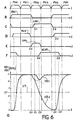
- the timing diagrams A to G of FIG. 5 represent the variations as a function of time of the different signals which have already been mentioned previously.
- the timing diagram A represents the four clock phases PH0, PH1, PH2, PH3 involved in the operation of a central computer unit.
- the timing diagram B represents the signal present on the NAC line described in FIG. 3.
- the timing diagram C represents the CAN signal originating from the flip-flop 44,45.
- the timing diagram D represents the complementary signal NEG of the control signal EG of the preload.
- the timing diagram E represents the selection signal SMi of a memory point connected to the bit lines.
- the timing diagram F represents the complementary signal NCAP of the control signal CAP coming from the detector 3 represented in FIGS. 1 and 2.
- the timing diagram G represents the variations as a function of time of the voltages VB0 and VB1 present respectively on the bit lines B0, B1.
- the variant embodiment corresponding to the operation represented in FIG. 5 corresponds to the case where the precharge circuit is constituted simply by an equalization transistor.
- phase PH2 Shortly before the appearance of phase PH2, at time t0, the bit lines B0, B1 are preloaded to a constant value equal to half of the supply voltage Vdd. On the timing diagram G, it was assumed that this voltage Vdd was equal to 5 volts. After the instant t0, the signal PH2 becoming active, the selection control circuit 2 delivers the signal SMi to the selection input of the memory point 1. This signal causes the memorizing circuits of the memory point 1 to communicate with bit lines B0, B1. As a result, the voltage of one of the bit lines will increase and that of the other bit line will decrease. On the timing diagram G, it was assumed that the voltage VB1 increased while the voltage VB0 decreased, indicating a memorized logic value 1.
- the transistor 42 of the circuit of FIG. 3 becomes conductive, which causes the discharge of the NAC line.
- the CAN output of flip-flop 44.45 changes to the logic value 1 at time t1, some time after time t0.
- the CAN signal then activates at the instant t1 the first amplifier AN which causes the accelerated discharge of the bit line B0 via the transistor N1.
- the second transistor N2 then being blocked or, at least, less conductive than the transistor N1, the voltage VB1 of line B1 remains constant or decreases less quickly than that of line B0.
- the voltage VB0 reaches at the instant t2 the value VT of triggering threshold of the detector 3, the latter delivers a signal CAP activating the second amplifier AN.
- the transistor P2 of the second amplifier AP becomes conductive.
- Line B1 is then loaded at the supply voltage Vdd via the transistors P3 and P2.
- the voltage VB1 increases rapidly until the supply voltage Vdd.
- the voltage VB0 continues to decrease to 0. This amplification continues throughout the phase PH3 until the next phase PH0.
- the signal PH0 then makes the transistor 43 of FIG. 3 conductive, thus causing the precharge of the NAC line to the supply voltage.
- the flip-flop 44,45 then changes state and the CAN signal takes the value 0 at time t3.
- the output signal EG of the equalization control circuit 5 then takes the value 0 at time t4. This results in the activation of the equalization transistor 57 of the precharge circuit PC and the line B1 discharges while the line B0 charges up to a common value approximately equal to half the supply voltage. This equalization continues throughout the next phase PH1.
- the second amplifier AP contributes to the preload between times t4 and t5, which is made possible precisely by the enslavement of its triggering by the voltage of the bit lines and not by a signal of outdoor clock.
- the two amplifiers AN and AP work symmetrically. However, if these amplifiers are made in MOS technology, it is then necessary to provide p-channel transistors as efficient as n-channel transistors to form the two amplifiers AN and AP. However, p-channel MOS transistors having performance equivalent to n-channel MOS transistors are much larger. It is therefore desirable to design a device which takes these technological constraints into account. It is therefore more advantageous to make the amplifier AN work more than the amplifier AP, which will make it possible to use less efficient p-channel transistors. For this, and according to another characteristic of the invention, the bit lines are no longer preloaded at a voltage half of the supply voltage Vdd but at the voltage Vdd itself. The precharging circuit PC which has been described in FIG. 4 allows this precharging at the supply voltage.
- the timing diagrams in Figure 6 explain the operation of the amplification device in the latter case.
- the timing diagrams A to G have the same meaning as those of FIG. 5.
- the operation will be as follows. As in the case of FIG. 5, during the phase PH2, at time t1 the first amplifier AN is activated. As before, line B0 is discharged via transistors N1 and N3. Taking into account the preload at the voltage Vdd the other line B1 also discharges but less quickly than the line B0. When the voltage VB0 reaches the threshold VT, the amplifier AP is activated and the line B1 is recharged at the supply voltage Vdd via the transistors P2 and P3 of the second amplifier AP. Finally, line B1 charges at the supply voltage and line B0 takes earth voltage.
- the precharge signal EG activates the precharge circuit PC.
- Line B1 then remains at the supply voltage while line B0 charges at this same voltage.
- the second amplifier AP contributes to the preload.
- the first amplifier AN has a much more important work than the second amplifier AP during the reading phase.
- the amplifier AP only has an auxiliary role which authorizes the use of a much less powerful PMOS transistor than in the case of a precharge at a voltage lower than the supply voltage. In return, PC preload requires more energy. However, this does not harm the overall performance of the circuit, the most important parameter of which is the speed of reading and amplification of the stored values.
Abstract
L'amplificateur comprend un premier (AN) et un second (AP) amplificateur sensibles aux tensions (VB0,VB1) des lignes de bits (B0,B1) à amplifier. Lorsqu'il est activé, le premier amplificateur (AN) met en communication avec la masse la ligne de bit ayant le plus faible potentiel. Lorsque la tension d'une des lignes de bit est inférieure à une valeur de seuil (VT), le second amplificateur est déclenché et met alors en communication la ligne de bit ayant le plus fort potentiel avec la tension d'alimentation. Utilisation pour réaliser des unités de traitement d'ordinateur en technologie CMOS.The amplifier comprises a first (AN) and a second (AP) amplifier sensitive to the voltages (VB0, VB1) of the bit lines (B0, B1) to be amplified. When activated, the first amplifier (AN) connects the bit line with the lowest potential to earth. When the voltage of one of the bit lines is less than a threshold value (VT), the second amplifier is triggered and then puts the bit line with the highest potential into communication with the supply voltage. Use to make computer processing units in CMOS technology.
Description
L'invention concerne un dispositif d'amplification, couramment appelé amplificateur de lecture, servant à amplifier la différence de tension apparaissant entre deux lignes et représentant un bit d'information.The invention relates to an amplification device, commonly called a reading amplifier, used to amplify the voltage difference appearing between two lines and representing an information bit.
De tels amplificateurs servent aussi à stabiliser les niveaux de tension des deux lignes de bit.Such amplifiers also serve to stabilize the voltage levels of the two bit lines.
Les lignes de bits peuvent être les lignes de sortie d'une cellule mémoire délivrant des niveaux de tension nécessitant une amplification. L'amplificateur de lecture selon l'invention peut s'appliquer aussi bien à des cellules mémoire statiques que dynamiques.The bit lines can be the output lines of a memory cell delivering voltage levels requiring amplification. The read amplifier according to the invention can be applied to both static and dynamic memory cells.
Les lignes de bits peuvent être également reliées aux lignes de sorties d'un circuit logique faisant partie d'un opérateur appartenant par exemple à une unité centrale de traitement d'un ordinateur.The bit lines can also be connected to the output lines of a logic circuit forming part of an operator belonging for example to a central processing unit of a computer.
L'amplificateur selon l'invention est particulièrement bien adapté pour amplifier les signaux de sortie de circuit réalisés en technologie CMOS.The amplifier according to the invention is particularly well suited for amplifying the circuit output signals produced in CMOS technology.
De façon classique, les amplificateurs de lecture doivent maintenir les deux lignes de bit à des niveaux de tension prédéterminés et stables représentatifs d'une valeur binaire correspondante. Habituellement l'un de ces niveaux correspond à la tension de masse du circuit tandis que l'autre niveau est celui d'une source de tension d'alimentation.Typically, the sense amplifiers must maintain the two bit lines at predetermined and stable voltage levels representative of a corresponding binary value. Usually one of these levels corresponds to the ground voltage of the circuit while the other level is that of a supply voltage source.
Les amplificateurs de lecture doivent satisfaire d'une part à une contrainte de rapidité de fonctionnement et d'autre part ils doivent être conçus pour réduire leur consommation le plus possible.The sense amplifiers must satisfy on the one hand a constraint of speed of operation and on the other hand they must be designed to reduce their consumption as much as possible.
Le brevet US-A-4551641 décrit un dispositif d'amplification en technologie CMOS constitué par un premier amplificateur réalisé à l'aide de transistors NMOS montés en croix qui, sous l'action d'un signal de commande, réalise la mise à la masse de la ligne de bit ayant la tension la plus proche de la tension de masse. Sous l'action d'un second signal de commande, un second amplificateur utilisant des transistors PMOS montés en croix a pour effet de mettre en communication la deuxième ligne de bit avec la source d'alimentation. Les signaux de commande des deux amplificateurs sont des signaux d'horloge déphasés entre eux. Ce dispositif réalise bien l'amplification des lignes de bits mais il exige la présence de deux signaux d'horloge dont le déphasage doit être suffisant pour activer le second amplificateur lorsque la première ligne de bit est suffisamment déchargée. En effet, si l'amplificateur à transistors PMOS était déclenché trop tôt, avant que la première ligne de bit soit suffisamment déchargée, les deux amplificateurs créeraient un chemin de court-circuit entre la source d'alimentation et la masse. Ceci constitue un inconvénient important dans le cas notamment où plusieurs dispositifs d'amplification sont utilisés pour amplifier la sortie d'un registre ou d'un opérateur comprenant un grand nombre de lignes de bit, chaque paire de lignes de bit étant reliée à un tel dispositif d'amplification commandé par des signaux provenant d'une horloge unique. Dans une telle application, tous les amplificateurs à transistors PMOS sont activés simultanément et il faut donc prévoir un retard suffisamment important entre cette activation et celle des amplificateurs à transistors NMOS de façon à éviter le court-circuit précité dans n'importe quelle paire de lignes de bit. De plus, ce retard doit tenir compte également de la dispersion des propriétés des circuits inhérente à la fabrication. Ces remarques montrent que l'on sera donc amené à exagérer le déphasage entre les activations des deux amplificateurs, ce qui entraînera nécessairement un fonctionnement moins rapide de l'amplification. Sinon, on augmentera le risque de créer des chemins de court-circuit entre l'alimentation et la masse, donc la consommation.The patent US-A-4551641 describes an amplification device in CMOS technology constituted by a first amplifier produced using NMOS transistors mounted in a cross which, under the action of a control signal, realizes the setting ground of the bit line having the voltage closest to the ground voltage. Under the action of a second control signal, a second amplifier using PMOS transistors mounted in cross has the effect of putting the second bit line in communication with the power source. The control signals of the two amplifiers are clock signals phase shifted between them. This device does the amplification of the bit lines well but it requires the presence of two clock signals whose phase shift must be sufficient to activate the second amplifier when the first bit line is sufficiently discharged. Indeed, if the PMOS transistor amplifier was triggered too early, before the first bit line was sufficiently discharged, the two amplifiers would create a short-circuit path between the power source and the ground. This constitutes an important drawback in the case in particular where several amplification devices are used to amplify the output of a register or of an operator comprising a large number of bit lines, each pair of bit lines being connected to such a amplification device controlled by signals from a single clock. In such an application, all the PMOS transistor amplifiers are activated simultaneously and it is therefore necessary to provide a sufficiently long delay between this activation and that of the NMOS transistor amplifiers so as to avoid the aforementioned short circuit in any pair of lines. debit. In addition, this delay must also take into account the dispersion of the properties of the circuits inherent in manufacturing. These remarks show that we will therefore have to exaggerate the phase shift between activations of the two amplifiers, which will necessarily lead to slower amplification operation. Otherwise, we will increase the risk of creating short-circuit paths between the power supply and the ground, therefore consumption.
L'invention a pour but d'éviter les inconvénients précités et pour cela propose un dispositif d'amplification selon lequel le second amp lificateur n'est pas commandé par un signal d'horloge mais par un signal dérivé de l'état des tensions sur les lignes de bits.The invention aims to avoid the aforementioned drawbacks and for this proposes an amplification device according to which the second amplifier is not controlled by a clock signal but by a signal derived from the state of the voltages on bit lines.
Plus précisément l'invention a pour objet un dispositif pour amplifier la différence de tension entre deux lignes de bit ledit dispositif étant associé à une source de tension d'alimentation et comprenant un premier amplificateur sensible aux tensions desdites lignes de bit et qui, lorsqu'il est activé par un signal de commande met en communication la ligne de bits ayant la plus faible tension avec la borne de plus faible potentiel de ladite source de tension, ledit dispositif étant caractérisé en ce qu'il comprend un circuit de détection délivrant un signal de sortie lorsque la tension d'une des lignes de bit est inférieure à une valeur déterminée et en ce que ledit signal de sortie commande l'activation d'un second amplificateur sensible auxdites tensions qui, lorsqu'il est activé, met en communication la ligne de bit ayant la tension la plus élevée avec la borne de plus fort potentiel de ladite source d'alimentation.More specifically, the subject of the invention is a device for amplifying the voltage difference between two bit lines, said device being associated with a supply voltage source and comprising a first amplifier sensitive to the voltages of said bit lines and which, when it is activated by a control signal communicates the bit line having the lowest voltage with the lowest potential terminal of said voltage source, said device being characterized in that it comprises a detection circuit delivering a signal output when the voltage of one of the bit lines is less than a determined value and in that said output signal controls the activation of a second amplifier sensitive to said voltages which, when activated, puts the communication into communication bit line having the highest voltage with the highest potential terminal of said power source.
L'invention propose également un mode de réalisation utilisant la technologie CMOS.The invention also proposes an embodiment using CMOS technology.
Selon un autre aspect, l'invention concerne également un dispositif permettant d'asservir l'activation du premier amplificateur aux signaux de sélection de la cellule mémoire ou de l'opérateur dont la sortie est amplifiée par des dispositifs selon l'invention.According to another aspect, the invention also relates to a device making it possible to subject the activation of the first amplifier to the cell selection signals memory or of the operator whose output is amplified by devices according to the invention.
Selon un autre aspect, le dispositif d'amplification selon l'invention est associé à un circuit permettant une précharge des lignes de bit asservie à la fin de l'activation du premier amplificateur.According to another aspect, the amplification device according to the invention is associated with a circuit allowing preload of the bit lines slaved at the end of the activation of the first amplifier.
D'autres caractéristiques et détails de réalisation apparaîtront dans le mode de réalisation préférentiel décrit dans la description qui va suivre :
- La figure 1 représente schématiquement un dispositif d'amplification selon l'invention.
- La figure 2 représente un mode de réalisation en technologie CMOS des circuits d'amplification et d'auto-déclenchement du dispositif d'amplification selon l'invention.
- La figure 3 représente un mode de réalisation d'un circuit de déclenchement du dispositif d'amplification selon l'invention.
- La figure 4 représente un circuit de précharge des lignes de bit faisant partie du dispositif d'amplification selon l'invention.
- Les figures 5 et 6 représentent des chronogrammes permettant d'expliquer le fonctionnement selon deux variantes de réalisation du dispositif d'amplification selon l'invention.
- FIG. 1 schematically represents an amplification device according to the invention.
- FIG. 2 represents an embodiment in CMOS technology of the amplification and self-triggering circuits of the amplification device according to the invention.
- FIG. 3 represents an embodiment of a trigger circuit of the amplification device according to the invention.
- FIG. 4 represents a circuit for precharging the bit lines forming part of the amplification device according to the invention.
- Figures 5 and 6 show timing diagrams to explain the operation according to two alternative embodiments of the amplification device according to the invention.
La figure 1 montre de façon schématique les éléments essentiels constituant le dispositif d'amplification. La figure montre également comment ce dispositif coopère avec un point mémoire ou un circuit logique binaire.Figure 1 shows schematically the essential elements constituting the amplification device. The figure also shows how this device cooperates with a memory point or a binary logic circuit.
La figure 1 représente les lignes de bits B0,B1 qui sont reliées aux bornes de sortie de l'unité binaire 1 qui est par exemple une bascule faisant partie d'un registre.FIG. 1 represents the bit lines B0, B1 which are connected to the output terminals of the
L'unité binaire 1 pourrait également être le circuit de sortie associé à un bit d'un opérateur numérique. Pour simplifier la suite de l'exposé, nous nous contenterons de désigner cette unité binaire par l'expression "point mémoire".The
Le point mémoire 1 est sélectionné par le signal SMi issu d'un circuit de sélection 2 recevant un signal de commande de lecture RD, un signal d'horloge PH2 et éventuellement un signal de sélection de registre SELi qui est utilisé si le point mémoire 1 est une bascule appartenant à un banc de registre. Dans le cas où le registre i du banc est sélectionné, le signal SELi devient actif, ce qui sélectionne toutes les bascules du registre i par le signal SMi. La sélection n'est effective que sous la commande du signal de lecture RD et pendant la phase de lecture imposée par le signal d'horloge PH2. Le circuit de sélection 2 ne pose pas de problème de réalisation particulier. Il est avantageusement réalisé de façon classique à l'aide de portes logiques en technologie CMOS.The
Le point mémoire 1 et le circuit de sélection 2 sont mentionnés dans le but de montrer le contexte dans lequel est placé le dispositif d'amplification de l'invention. Le dispositif d'amplification proprement-dit est constitué par un premier amplificateur AN relié aux lignes de bit B0,B1 et activé par un signal de commande CAN. L'activation de l'amplificateur AN a pour effet de décharger la ligne de bit B0 ou B1 ayant le plus faible potentiel. Par exemple si le circuit travaille entre les tensions 0 et 5 volts, l'amplificateur AN mettra en communication la ligne de plus faible potentiel avec la masse.The
Le signal de commande CAN est généré par le circuit de commande 4 en réponse au signal de commande de lecture RD pendant la phase de lecture déterminée par le signal d'horloge PH2.The CAN control signal is generated by the
Un second amplificateur AP est connecté également aux lignes de bit B0,B1 et reçoit le signal de commande CAP. Lorsqu'il est activé, cet amplificateur AP a pour effet de charger la ligne ayant le plus fort potentiel. Par exemple, si la tension d'alimentation est de 5 volts, la ligne de plus fort potentiel sera chargée à 5 volts par l'amplificateur AP.A second amplifier AP is also connected to the bit lines B0, B1 and receives the control signal CAP. When activated, this AP amplifier has the effect of charging the line with the highest potential. For example, if the supply voltage is 5 volts, the line with the highest potential will be charged at 5 volts by the AP amplifier.
Le signal de commande CAP du second amplificateur AP est fourni par un circuit de détection 3 dont les entrées sont reliées aux deux lignes de bit B0,B1. Le détecteur 3 active le signal CAP lorsque l'une des tensions VB0,VB1 des lignes de bits B0,B1 est en-dessous d'un seuil de tensions prédéterminées. Ainsi, grâce au détecteur 3, le second amplificateur AP est auto-déclenché, c'est-à-dire déclenché automatiquement lorsque le premier amplificateur a travaillé suffisamment pour décharger la ligne de bit de plus faible potentiel. L'échelonnement des déclenchements des deux amplificateurs AN,AP est indispensable pour garantir une amplification stable de la différence de la tension relativement faible présente initialement entre les deux lignes de bit.The control signal CAP of the second amplifier AP is supplied by a
De façon classique, le dispositif d'amplification comprend également un circuit de précharge PC destiné à précharger les deux lignes de bit à une tension déterminée avant une sélection du point mémoire pour sa lecture. Le circuit de précharge PC est actionné par le signal de commande EG issu d'un circuit de commande de précharge 5. Ce circuit de commande de précharge reçoit le signal de commande CAN du premier amplificateur AN. Ce circuit reçoit également le signal d'horloge PH0 qui détermine la phase de précharge. Ce signal d'horloge PH0 est également appliqué au circuit de commande 4 du premier amplificateur AN et a pour effet de désactiver le signal de commande CAN du premier amplificateur AN. Le circuit de commande de précharge 5 a pour rôle d'asservir l'activation de la précharge au signal CAN de sorte que le signal de commande de précharge ne soit actif qu'après la disparition du signal de commande de l'amplificateur AN.Conventionally, the amplification device also comprises a precharge circuit PC intended for precharging the two bit lines at a determined voltage before a selection of the memory point for its reading. The precharge circuit PC is actuated by the control signal EG from a
Le fonctionnement du dispositif de la figure 1 est le suivant. Nous nous placons dans le cas où les circuits sont alimentés par une source de tension positive de 5 volts par exemple. Dès l'apparition du signal PH0, le signal CAN est mis à zéro par le circuit 4. Dès que le signal CAN est à zéro, le circuit 5 délivre le signal de commande de précharge EG qui active le circuit de précharge PC. Les lignes de bit B0,B1 sont alors chargées à la même tension de précharge. Durant la phase de lecture définie par le signal PH2, si les signaux RD et SELi sont appliqués au circuit de commande de sélection 2, le point mémoire 1 est sélectionné par le signal SMi. En fonction de la valeur binaire mémorisée dans le point mémoire 1, l'une des lignes de bit prendra une tension supérieure à la tension de l'autre ligne de bit. D'autre part, le circuit de commande 4 provoquera l'activation du premier amplificateur AN. Il en résulte alors une décharge de la ligne de bit qui avait la plus faible tension. Lorsque la tension de cette ligne descend en dessous d'une valeur seuil, cet état est détecté par le circuit 3 qui active alors le second amplificateur AP. La ligne de bit ayant la plus forte tension est alors chargée à la tension d'alimentation par le second amplificateur. Ainsi grâce à l'action conjuguée des deux amplificateurs l'une des lignes de bit aura la tension nulle tandis que l'autre ligne de bit sera portée à la tension d'alimentation. Cet état subsistera jusqu'à l'apparition d'une nouvelle phase de précharge PH0.The operation of the device of Figure 1 is as follows. We place ourselves in the case where the circuits are supplied by a positive voltage source of 5 volts for example. As soon as the signal PH0 appears, the CAN signal is set to zero by the
Tout en restant dans le cadre de l'invention, on peut concevoir également de permuter les rôles des deux amplificateurs AP et AN. Selon cette variante, l'amplificateur AP est d'abord activé par le signal CAN. Lorsque la tension de la ligne ayant le plus fort potentiel dépasse une valeur de seuil, le détecteur active alors l'amplificateur AN.While remaining within the scope of the invention, it is also conceivable to permute the roles of the two amplifiers AP and AN. According to this variant, the amplifier AP is first activated by the CAN signal. When the voltage of the line with the highest potential exceeds a threshold value, the detector then activates the amplifier AN.
La figure 2 représente un mode de réalisation détaillée du premier amplificateur AN, du second amplificateur AP et du détecteur 3 qui le commande. Les circuits sont réalisés au moyen de transistors à effet de champs tels que des transistors MOS. Plus précisément la réalisation est faite en technologie CMOS. Par convention, les transistors PMOS se distinguent des transistors NMOS par un petit rond accolé à leur grille.FIG. 2 represents a detailed embodiment of the first amplifier AN, the second amplifier AP and the
Les deux amplificateurs AN et AP utilisent un montage classique. Le premier amplificateur AN est réalisé au moyen de trois transistors NMOS. Un premier transistor N1 a son drain relié à une des lignes de bit B0, un second transistor N2 a son drain relié à l'autre ligne de bit B1 et les sources des deux transistors N1,N2 sont reliées au drain d'un troisième transistor N3 dont la source est reliée à la masse. La grille du premier transistor est reliée à la second ligne de bit B1 tandis que la grille de deuxième transistor est reliée à la première ligne de bit B0. La grille du troisième transistor N3 reçoit le signal de commande CAN. Le second amplificateur AP utilise des transistors PMOS montés de façon analogue. Un premier transistor P1 a son drain relié à la première ligne de bit B0, un second transistor P2 a son drain relié à la première ligne de bit B0, les sources de ces deux transistors P1,P2 sont reliées au drain d'un troisième transistor P3 dont la source est reliée à la tension d'alimentation Vdd. Le troisième transistor P3 reçoit sur sa grille le signal de commande CAP.The two amplifiers AN and AP use a conventional arrangement. The first AN amplifier is made using three NMOS transistors. A first transistor N1 has its drain connected to one of the bit lines B0, a second transistor N2 has its drain connected to the other bit line B1 and the sources of the two transistors N1, N2 are connected to the drain of a third transistor N3 whose source is connected to ground. The gate of the first transistor is connected to the second bit line B1 while the gate of the second transistor is connected to the first bit line B0. The gate of the third transistor N3 receives the CAN control signal. The second AP amplifier uses PMOS transistors similarly mounted. A first transistor P1 has its drain connected to the first bit line B0, a second transistor P2 has its drain connected to the first bit line B0, the sources of these two transistors P1, P2 are connected to the drain of a third transistor P3 whose source is connected to the supply voltage Vdd. The third transistor P3 receives on its gate the control signal CAP.
Le détecteur 3 est constitué par une porte logique ET réalisée en technologie CMOS. Pour réaliser une porte ET on utilise une porte "NON ET" CMOS suivie d'un inverseur CMOS. Comme représenté à la figure 2, la porte "NON ET" est constituée par les quatre transistors DP1,DP2,DN1,DN2 montés de façon classique. Deux transistors PMOS DP1,DP2 sont montés en parallèle, leurs sources étant reliées à la tension d'alimentation positive Vdd. Deux transistors NMOS DN1,DN2 sont montés en série, le drain du transistor DN1 étant relié aux drains des transistors DP1 et DP2, la source du transistor DN2 étant reliée à la masse. Les grilles des transistors DN1 et DP1 sont reliées à la ligne. B1, celles des transistors DN2 et DP2 à la ligne B0. L'inverseur est réalisé par les deux transistors complémentaires DP3,DN3, selon un montage classique.The
Le fonctionnement du circuit de la figure 2 est le suivant. Si l'on suppose qu'au moment de la commande du premier amplificateur AN la tension de la ligne de bit B0 est inférieure à celle de la ligne de bit B1, le transistor à canal n N1 est davantage conducteur que le transistor N2. Il en résulte que la tension de la ligne B0 décroit plus rapidement que celle de la ligne B1. Lorsque la tension de la ligne B0 est inférieure à la tension de seuil du transistor à canal n DN2 du détecteur 3, ce dernier transistor est bloqué. D'autre part, la tension de la ligne B0 appliquée à la grille du transistor complémentaire DP2 rend ce dernier transistor à l'état passant. La tension NCAP du drain de ce transistor augmente alors vers la tension d'alimentation Vdd. Il en résulte que la tension de sortie CAP de l'inverseur DP3,DN3 décroit vers 0. Le transistor à canal p P3 de l'amplificateur AP devient alors conducteur et compt e tenu de la différence de tension présente entre les lignes de bits B0,B1, le transistor à canal p P2 deviendra conducteur tandis que le second transistor à canal p P1 sera moins conducteur. La tension VB1 de la ligne de bit B1 augmentera donc vers la tension d'alimentation Vdd. Simultanément le transistor à canal p P1 deviendra de moins en moins conducteur. Finalement la ligne de bit B1 sera chargée à la tension d'alimentation Vdd, tandis que la ligne de bit B0 sera complètement déchargée.The operation of the circuit of FIG. 2 is as follows. If it is assumed that when the first amplifier AN is controlled the voltage of the bit line B0 is lower than that of the bit line B1, the n-channel transistor N1 is more conductive than the transistor N2. As a result, the voltage of line B0 decreases faster than that of line B1. When the voltage of line B0 is less than the threshold voltage of the n-channel transistor DN2 of
Un fonctionnement analogue est obtenu dans l'hypothèse où la tension de la ligne de bit B1 est inférieure à la ligne de bit B0. Dans ce dernier cas, le transistor à canal p DP1 du détecteur 3 devient conducteur lorsque la tension VB1 de la ligne de bit B1 est inférieure à la tension de seuil de ce transistor. De même, le transistor à canal n DN1 sera bloqué. Il en résulte comme précédemment l'activation du second amplificateur AP. Finalement la tension VB1 devient nulle et la tension VB0 devient égale à la tension d'alimentation Vdd.A similar operation is obtained on the assumption that the voltage of the bit line B1 is lower than the bit line B0. In the latter case, the p-channel transistor DP1 of the
Dans la mesure où les fonctionnements des amplificateurs AN et AP ne seraient pas fondamentalement modifiés, leurs réalisations pourraient subir des modifications mineures pour des raisons purement technologique. En particulier, on peut remplacer le transistor N3 par deux transistors de type n en parallèle. De même les sources dex transistors P1 et P2 pourraient être reliés séparément à la source de tension par l'intermédiaire, respectivement, de deux transistors de type p commandés par le même signal CAP.Insofar as the operations of the amplifiers AN and AP would not be fundamentally modified, their realizations could undergo minor modifications for purely technological reasons. In particular, the transistor N3 can be replaced by two n-type transistors in parallel. Likewise the sources of the transistors P1 and P2 could be connected separately to the voltage source via, respectively, two p-type transistors controlled by the same signal CAP.
La figure 3 représente un mode de réalisation du circuit de commande 4 du premier amplificateur AN. Ce circuit comprend une porte ET 41 recevant le signal de commande de lecture RD et le signal d'horloge PH2 commandant la phase de lecture. La sortie de cette porte ET 41 est reliée à la grille d'un transistor NMOS 42 dont la source est reliée à la masse et dont le drain est relié à une ligne NAC. Cette ligne NAC est reliée à l'entrée d'une bascule constituée par deux inverseurs CMOS montés en tête-bêche 44,45. La sortie de cette bascule délivre le signal de commande CAN du premier amplificateur AN. La ligne NAC est également reliée au drain d'un transistor PMOS 43 dont la source est reliée à la tension d'alimentation Vdd et dont la grille reçoit le signal NPH0. La ligne NAC peut également être reliée au drain d'un ou plusieurs transistors NMOS 46 dont la grille reçoit un signal T.FIG. 3 represents an embodiment of the
Ce circuit de commande fonctionne de la façon suivante. Pendant la phase de précharge, le signal d'horloge PH0 est actif et son signal complémentaire NPH0 appliqué à la grille du transistor 43 rend ce dernier conducteur. Il en résulte que la ligne NAC se charge à la tension d'alimentation Vdd. La sortie de la bascule 44,45 prend alors la valeur 0 logique correspondant à une tension nulle et le premier amplificateur AN n'est pas activé. Pendant la phase de lecture, le signal d'horloge PH2 est actif. Si en même temps le signal RD est actif, le signal de sortie de la porte ET 41 rend conducteur le transistor 42, ce qui décharge la ligne NAC. Il en résulte que la bascule 44,45 change d'état et son signal de sortie CAN prend la valeur 1 logique correspondant à la tension Vdd, activant ainsi le premier amplificateur AN.This control circuit operates as follows. During the precharge phase, the clock signal PH0 is active and its complementary signal NPH0 applied to the gate of
La commutation du transistor 42, la décharge de la ligne NAC et le changement d'état de la bascule 44,45 nécessite un certain délai qui a pour effet de retarder l'activation du premier amplificateur par rapport à l'apparition du signal d'horloge PH2. Ainsi l'amplificateur AN sera activé un certain temps après la sélection du point mémoire 1, ce qui laisse un temps suffisant pour que les lignes de bit B0,B1 présentent une différence de tension qui permette un fonctionnement correct du premier amplificateur AN.The switching of the
Le transistor 46 est prévu pour permettre l'activation des amplificateurs AN en dehors du cas d'une lecture. Ceci peut être utile si on veut utiliser les lignes de bit B0,B1 simplement comme lignes de transfert sans sélection d'un point mémoire associé à ces lignes.The
La figure 4 représente un mode de réalisation d'un dispositif permettant la précharge des lignes de bit B0,B1. Ce dispositif se compose du circuit de précharge proprement-dit PC et d'un circuit de commande 5.FIG. 4 represents an embodiment of a device allowing the precharging of the bit lines B0, B1. This device consists of the actual preload circuit PC and a
Le circuit de précharge PC est constitué par trois transistors à effet de champs à canal p 55,56,57. Les deux transistors 55 et 56 ont leur source reliée à une borne d'alimentation de tension positive, Vdd par exemple. Les drains des transistors 55 et 56 sont reliés respectivement aux deux lignes de bit B0,B1. Le troisième transistor 57 a ses électrodes de courant reliées aux deux lignes de bit B0,B1. Les trois transistors 55 56 et 57 reçoivent sur leur grille le signal EG issu du circuit de commande 5.The PC precharge circuit consists of three p-channel
Le fonctionnement du circuit de précharge PC est très simple. Lorsque le signal EG prend la valeur 1 logique correspondant à la tension Vdd, les trois transistors 55, 56, 57 sont bloqués. Lorsque le signal EG prend la valeur 0 logique, les trois transistors conduisent. Il en résulte que les lignes de bit B0,B1 vont se charger à la tension d'alimentation Vdd, le transistor 57 garantissant une égalisation des tensions des deux lignes.The operation of the PC precharge circuit is very simple. When the signal EG takes the
La précharge des lignes de bit B0 et B1 ne doit pas s'opérer lorsque le premier amplificateur AN est encore actif car sinon cela provoquerait un chemin de court-circuit entre la tension positive Vdd et la masse via l'un des transistors 55 ou 56 du circuit de précharge PC et l'un des transistors N1 ou N2 à l'état passant du premier amplificateur AN. Dans ce but le circuit de commande de précharge 5 comprend une porte OU 51 recevant sur ses deux entrées le signal CAN et le signal complémentaire NPH0 du signal d'horloge PH0 servant à déclencher la phase de précharge. La sortie de la porte OU 51 est reliée à l'une des deux entrées d'une porte ET 52 dont l'autre entrée reçoit le signal complémentaire NPH1 d'un autre signal d'horloge PH1, succèdant au signal PH0. La sortie de la porte ET 52 fournit le signal EG appliqué aux grilles des transistors du circuit de précharge PC.The preload of bit lines B0 and B1 must not take place when the first amplifier AN is still active because otherwise it would cause a short-circuit path between the positive voltage Vdd and the ground via one of the
Le circuit de commande 5 permet donc l'activation du circuit de précharge PC alors que le signal d'horloge PH0 est actif mais à condition seulement que le signal CAN soit déjà inactif. Ce dispositif permet donc le déclenchement de la précharge le plus tôt possible au début de la phase de précharge PH0, tout en tenant compte du retard pour la désactivation du signal CAN provoqué par les temps de réponse du transistor 43 et de la bascule 44,45 décrit à la figure 3.The
La porte ET 52 qui reçoit le signal NPH1 a été mentionnée pour tenir compte du cas où le dispositif d'amplification est utilisé dans une unité centrale de traitement d'ordinateur travaillant en quatre phases d'horloge. Plus précisément, la première phase d'horloge PH0 correspond à une phase de désactivation des amplificateurs de chemin de données et à la précharge de la ligne de contrôle NAC mentionnée à la figure 3. La phase PH1 est une phase dédiée à la précharge des lignes de bit du chemin de donnée. La phase PH2 active la sélection des points mémoire ou des opérateurs numériques. Enfin une quatrième phase PH3 correspond à une phase d'amplification des signaux de sortie de ces points mémoires ou de ces circuits logiques.The AND
Il est à noter que l'on pourrait précharger les lignes de bit à des tensions inférieures à la tension positive Vdd de la source d'alimentation. On pourrait même simplifier le circuit de précharge en ne conservant que le seul transistor d'égalisation 57 car la sélection d'un point mémoire en lecture est toujours suivie d'une charge à la tension positive d'alimentation d'une des lignes de bits. L'activation du seul transistor d'égalisation 57 après une telle précharge placerait chacune des lignes de bit à une tension moitié de la tension d'alimentation.It should be noted that the bit lines could be precharged at voltages lower than the positive voltage Vdd of the power source. We could even simplify the precharge circuit by keeping only the single equalization transistor 57 because the selection of a read memory point is always followed by a charge at the positive supply voltage of one of the bit lines . Activation of the single equalization transistor 57 after such a precharge would place each of the bit lines at half the supply voltage.
Les chronogrammes représentés aux figures 5 et 6 vont permettre d'expliquer le fonctionnement détaillé du dispositif d'amplification selon l'invention selon deux variantes de réalisation du circuit de précharge.The timing diagrams shown in Figures 5 and 6 will explain the detailed operation of the amplification device according to the invention according to two alternative embodiments of the precharge circuit.
Les chronogrammes A à G de la figure 5 représentent les variations en fonction du temps des différents signaux qui ont été déjà mentionnés précédemment.The timing diagrams A to G of FIG. 5 represent the variations as a function of time of the different signals which have already been mentioned previously.
Le chronogramme A représente les quatre phases d'horloge PH0,PH1,PH2,PH3 intervenant dans le fonctionnement d'une unité centrale d'ordinateur. Le chronogramme B représente le signal présent sur la ligne NAC décrit à la figure 3. Le chronogramme C représente le signal CAN issu de la bascule 44,45. Le chronogramme D représente le signal complémentaire NEG du signal de commande EG de la précharge. Le chronogramme E représente le signal de sélection SMi d'un point mémoire connecté aux lignes de bit. Le chronogramme F représente le signal complémentaire NCAP du signal de commande CAP issu du détecteur 3 représenté aux figures 1 et 2. Enfin le chronogramme G représente les variations en fonction du temps des tensions VB0 et VB1 présentes respectivement sur les lignes de bit B0,B1.The timing diagram A represents the four clock phases PH0, PH1, PH2, PH3 involved in the operation of a central computer unit. The timing diagram B represents the signal present on the NAC line described in FIG. 3. The timing diagram C represents the CAN signal originating from the flip-
La variante de réalisation correspondant au fonctionnement représenté à la figure 5 correspond au cas où le circuit de précharge est constitué simplement par un transistor d'égalisation.The variant embodiment corresponding to the operation represented in FIG. 5 corresponds to the case where the precharge circuit is constituted simply by an equalization transistor.
Peu de temps avant l'apparition de la phase PH2, à l'instant t0, les lignes de bit B0,B1 sont préchargés à une valeur constante égale à la moitié de la tension d'alimentation Vdd. Sur le chronogramme G, il a été supposé que cette tension Vdd était égale à 5 volts. Après l'instant t0, le signal PH2 devenant actif, le circuit de commande de sélection 2 délivre le signal SMi à l'entrée de sélection du point mémoire 1. Ce signal provoque la mise en communication des circuits de mémorisation du point mémoire 1 avec les lignes de bits B0,B1. Il en résulte que la tension d'une des lignes de bits va augmenter et celle de l'autre ligne de bit va diminuer. Sur le chronogramme G, il a été supposé que la tension VB1 augmentait tandis que la tension VB0 diminuait, indiquant une valeur 1 logique mémorisée.Shortly before the appearance of phase PH2, at time t0, the bit lines B0, B1 are preloaded to a constant value equal to half of the supply voltage Vdd. On the timing diagram G, it was assumed that this voltage Vdd was equal to 5 volts. After the instant t0, the signal PH2 becoming active, the
D'autre part, à l'apparition du signal d'horloge PH2, le transistor 42 du circuit de la figure 3 devient conducteur ce qui provoque la décharge de la ligne NAC. Il en résulte que la sortie CAN de la bascule 44,45 passe à la valeur 1 logique à l'instant t1, quelque temps après l'instant t0. Le signal CAN active alors à l'instant t1 le premier amplificateur AN ce qui provoque la décharge accélérée de la ligne de bit B0 par l'intermédiaire du transistor N1.On the other hand, when the clock signal PH2 appears, the
Le second transistor N2 étant alors bloqué ou, tout au moins, moins conducteur que le transistor N1, la tension VB1 de la ligne B1 reste constante ou décroit moins vite que celle de la ligne B0. Lorsque la tension VB0 atteint à l'instant t2 la valeur VT de seuil de déclenchement du détecteur 3, ce dernier délivre un signal CAP activant le second amplificateur AN. Il en résulte que le transistor P2 du second amplificateur AP devient conducteur. La ligne B1 est alors chargée à la tension d'alimentation Vdd par l'intermédiaire des transistors P3 et P2. Ainsi, à partir de l'instant t2, la tension VB1 augmente rapidement jusqu'à la tension d'alimentation Vdd. Simultanément, la tension VB0 continue à diminuer jusqu'à 0. Cette amplification continue durant toute la phase PH3 jusqu'à la phase suivante PH0. Le signal PH0 rend alors conducteur le transistor 43 de la figure 3 provoquant ainsi la précharge de la ligne NAC à la tension d'alimentation. La bascule 44,45 change ensuite d'état et le signal CAN prend la valeur 0 à l'instant t3. Le signal de sortie EG du circuit de commande d'égalisation 5 prend alors la valeur 0 à l'instant t4. Il en résulte l'activation du transistor d'égalisation 57 du circuit de précharge PC et la ligne B1 se décharge tandis que la ligne B0 se charge jusqu'à une valeur commune environ égale à la moitié de la tension d'alimentation. Cette égalisation de poursuit durant toute la phase suivante PH1.The second transistor N2 then being blocked or, at least, less conductive than the transistor N1, the voltage VB1 of line B1 remains constant or decreases less quickly than that of line B0. When the voltage VB0 reaches at the instant t2 the value VT of triggering threshold of the
Il est intéressant de n oter que le second amplificateur AP contribue à la précharge entre les instants t4 et t5, ce qui est rendu possible précisément par l'asservissement de son déclenchement par la tension des lignes de bit et non pas par un signal d'horloge extérieur.It is interesting to note that the second amplifier AP contributes to the preload between times t4 and t5, which is made possible precisely by the enslavement of its triggering by the voltage of the bit lines and not by a signal of outdoor clock.
Selon le fonctionnement décrit précédemment, nous constatons que les deux amplificateurs AN et AP travaillent symétriquement. Or, si ces amplificateurs sont réalisés en technologie MOS, il est alors nécessaire de prévoir des transistors à canal p aussi performants que des transistors à canal n pour constituer les deux amplificateurs AN et AP. Or des transistors MOS à canal p ayant des performances équivalentes à des transistors MOS à canal n sont beaucoup plus volumineux. Il est donc souhaitable de concevoir un dispositif tenant compte de ces contraintes technologiques. Il est donc plus avantageux de faire travailler davantage l'amplificateur AN que l'amplificateur AP, ce qui permettra d'utiliser des transistors à canal p moins performants. Pour cela, et selon une autre caractéristique de l'invention, les lignes de bits ne sont plus préchargées à une tension moitié de la tension d'alimentation Vdd mais à la tension Vdd elle-même. Le circuit de précharge PC qui a été décrit à la figure 4 permet cette précharge à la tension d'alimentation.According to the operation described above, we note that the two amplifiers AN and AP work symmetrically. However, if these amplifiers are made in MOS technology, it is then necessary to provide p-channel transistors as efficient as n-channel transistors to form the two amplifiers AN and AP. However, p-channel MOS transistors having performance equivalent to n-channel MOS transistors are much larger. It is therefore desirable to design a device which takes these technological constraints into account. It is therefore more advantageous to make the amplifier AN work more than the amplifier AP, which will make it possible to use less efficient p-channel transistors. For this, and according to another characteristic of the invention, the bit lines are no longer preloaded at a voltage half of the supply voltage Vdd but at the voltage Vdd itself. The precharging circuit PC which has been described in FIG. 4 allows this precharging at the supply voltage.
Les chronogrammes de la figure 6 permettent d'expliquer le fonctionnement du dispositif d'amplification dans ce dernier cas. Les chronogrammes A à G ont la même signification que ceux de la figure 5. Le fonctionnement sera le suivant. Comme dans le cas de la figure 5, au cours de la phase PH2, à l'instant t1 le premier amplificateur AN est activé. Comme précédemment, la ligne B0 se décharge par l'intermédiaire des transistors N1 et N3. Compte-tenu de la précharge à la tension Vdd l'autre ligne B1 se décharge également mais moins rapidement que la ligne B0. Lorsque la tension VB0 atteint la seuil VT, l'amplificateur AP est activé et la ligne B1 est rechargée à la tension d'alimentation Vdd par l'intermédiaire des transistors P2 et P3 du second amplificateur AP. Finalement, la ligne B1 se charge à la tension d'alimentation et la ligne B0 prend la tension de masse. Comme précédemment, à l'instant t4 de la phase PH0, le signal de précharge EG active le circuit de précharge PC. La ligne B1 reste alors à la tension d'alimentation tandis que la ligne B0 se charge à cette même tension. Selon cette variante également, le second amplificateur AP contribue à la précharge.The timing diagrams in Figure 6 explain the operation of the amplification device in the latter case. The timing diagrams A to G have the same meaning as those of FIG. 5. The operation will be as follows. As in the case of FIG. 5, during the phase PH2, at time t1 the first amplifier AN is activated. As before, line B0 is discharged via transistors N1 and N3. Taking into account the preload at the voltage Vdd the other line B1 also discharges but less quickly than the line B0. When the voltage VB0 reaches the threshold VT, the amplifier AP is activated and the line B1 is recharged at the supply voltage Vdd via the transistors P2 and P3 of the second amplifier AP. Finally, line B1 charges at the supply voltage and line B0 takes earth voltage. As before, at time t4 of phase PH0, the precharge signal EG activates the precharge circuit PC. Line B1 then remains at the supply voltage while line B0 charges at this same voltage. According to also this variant, the second amplifier AP contributes to the preload.
Comme nous pouvons le constater d'après l'allure des courbes VB1 et VB0 du chronogramme G de la figure 6 et contrairement à la variante précédente, le premier amplificateur AN a un travail beaucoup plus important que le second amplificateur APpendant la phase de lecture. L'amplificateur AP n'a plus qu'un rôle auxiliaire qui autorise l'utilisation de transistor PMOS beaucoup moins puissant que dans le cas d'une précharge à une tension inférieure à la tension d'alimentation. En contre-partie, la précharge PC exige davantage d'énergie. Mais cela ne nuit pas aux performances globales du circuit dont le paramètre le plus important est la rapidité de lecture et d'amplification des valeurs mémorisées.As we can see from the shape of the curves VB1 and VB0 of the timing diagram G in Figure 6 and unlike the previous variant, the first amplifier AN has a much more important work than the second amplifier AP during the reading phase. The amplifier AP only has an auxiliary role which authorizes the use of a much less powerful PMOS transistor than in the case of a precharge at a voltage lower than the supply voltage. In return, PC preload requires more energy. However, this does not harm the overall performance of the circuit, the most important parameter of which is the speed of reading and amplification of the stored values.
L'exposé qui précède montre que l'invention est particulièrement bien adaptée à une réalisation exécutée en totalité avec la technologie CMOS ou analogue. Bien entendu des modifications évidentes peuvent être apportées à l'invention. En particulier il est possible d'utiliser des sources d'alimentation ayant des tensions négatives ou remplacer un transistor quelconque par plusieurs transistors de même type en parallèle. The foregoing description shows that the invention is particularly well suited to an embodiment executed entirely with CMOS technology or the like. Obviously, obvious modifications can be made to the invention. In particular, it is possible to use power sources having negative voltages or to replace any transistor by several transistors of the same type in parallel.
Claims (11)
Applications Claiming Priority (2)
| Application Number | Priority Date | Filing Date | Title |
|---|---|---|---|
| FR8612221A FR2603414B1 (en) | 1986-08-29 | 1986-08-29 | READING AMPLIFIER |
| FR8612221 | 1986-08-29 |
Publications (2)
| Publication Number | Publication Date |
|---|---|
| EP0262013A1 true EP0262013A1 (en) | 1988-03-30 |
| EP0262013B1 EP0262013B1 (en) | 1991-01-23 |
Family
ID=9338585
Family Applications (1)
| Application Number | Title | Priority Date | Filing Date |
|---|---|---|---|
| EP87401936A Expired - Lifetime EP0262013B1 (en) | 1986-08-29 | 1987-08-27 | Sense amplifier |
Country Status (5)
| Country | Link |
|---|---|
| US (1) | US4810910A (en) |
| EP (1) | EP0262013B1 (en) |
| JP (1) | JPS6369095A (en) |
| DE (1) | DE3767635D1 (en) |
| FR (1) | FR2603414B1 (en) |
Families Citing this family (17)
| Publication number | Priority date | Publication date | Assignee | Title |
|---|---|---|---|---|
| JPH0469896A (en) * | 1990-07-10 | 1992-03-05 | Sharp Corp | Sense amplifying circuit |
| KR920013458A (en) * | 1990-12-12 | 1992-07-29 | 김광호 | Differential Detection Amplifier |
| JPH05217387A (en) * | 1992-02-05 | 1993-08-27 | Mitsubishi Electric Corp | Semiconductor memory device |
| US5471188A (en) * | 1994-10-07 | 1995-11-28 | International Business Machines Corporation | Fast comparator circuit |
| KR0171954B1 (en) * | 1995-06-30 | 1999-03-30 | 김주용 | Data bus driving circuit |
| DE19536486C2 (en) * | 1995-09-29 | 1997-08-07 | Siemens Ag | Evaluator and amplifier circuit |
| US5852373A (en) * | 1996-09-30 | 1998-12-22 | International Business Machines Corporation | Static-dynamic logic circuit |
| US5917771A (en) * | 1997-11-03 | 1999-06-29 | Arm Limited | Register bank bit lines |
| US11308383B2 (en) | 2016-05-17 | 2022-04-19 | Silicon Storage Technology, Inc. | Deep learning neural network classifier using non-volatile memory array |
| US10803943B2 (en) | 2017-11-29 | 2020-10-13 | Silicon Storage Technology, Inc. | Neural network classifier using array of four-gate non-volatile memory cells |
| US11087207B2 (en) * | 2018-03-14 | 2021-08-10 | Silicon Storage Technology, Inc. | Decoders for analog neural memory in deep learning artificial neural network |
| US10699779B2 (en) | 2017-11-29 | 2020-06-30 | Silicon Storage Technology, Inc. | Neural network classifier using array of two-gate non-volatile memory cells |
| US10748630B2 (en) | 2017-11-29 | 2020-08-18 | Silicon Storage Technology, Inc. | High precision and highly efficient tuning mechanisms and algorithms for analog neuromorphic memory in artificial neural networks |
| US11500442B2 (en) | 2019-01-18 | 2022-11-15 | Silicon Storage Technology, Inc. | System for converting neuron current into neuron current-based time pulses in an analog neural memory in a deep learning artificial neural network |
| US11023559B2 (en) | 2019-01-25 | 2021-06-01 | Microsemi Soc Corp. | Apparatus and method for combining analog neural net with FPGA routing in a monolithic integrated circuit |
| US11270771B2 (en) | 2019-01-29 | 2022-03-08 | Silicon Storage Technology, Inc. | Neural network classifier using array of stacked gate non-volatile memory cells |
| US11423979B2 (en) | 2019-04-29 | 2022-08-23 | Silicon Storage Technology, Inc. | Decoding system and physical layout for analog neural memory in deep learning artificial neural network |
Citations (4)
| Publication number | Priority date | Publication date | Assignee | Title |
|---|---|---|---|---|
| GB2070372A (en) * | 1980-01-31 | 1981-09-03 | Tokyo Shibaura Electric Co | Semiconductor memory device |
| EP0143591A2 (en) * | 1983-11-23 | 1985-06-05 | Motorola, Inc. | Sense amplifier |
| EP0175880A2 (en) * | 1984-09-21 | 1986-04-02 | Kabushiki Kaisha Toshiba | Semiconductor memory device |
| EP0185451A2 (en) * | 1984-12-13 | 1986-06-25 | Kabushiki Kaisha Toshiba | Semiconductor memory device with sense amplifiers |
Family Cites Families (8)
| Publication number | Priority date | Publication date | Assignee | Title |
|---|---|---|---|---|
| US4169233A (en) * | 1978-02-24 | 1979-09-25 | Rockwell International Corporation | High performance CMOS sense amplifier |
| JPS59186188A (en) * | 1983-04-07 | 1984-10-22 | Fujitsu Ltd | Sense amplifier |
| US4723228B1 (en) * | 1983-08-31 | 1998-04-21 | Texas Instruments Inc | Memory decoding circuitry |
| JPS60147997A (en) * | 1984-01-11 | 1985-08-05 | Toshiba Corp | Semiconductor storage device |
| US4561702A (en) * | 1984-05-09 | 1985-12-31 | Texas Instruments Incorporated | CMOS Address buffer circuit |
| JPS6132298A (en) * | 1984-07-23 | 1986-02-14 | Nec Corp | Sensor amplifier for employing complementary misfet |
| JPS61175880A (en) * | 1985-01-31 | 1986-08-07 | Matsushita Electric Ind Co Ltd | Broken line extracting device |
| JPS61185451A (en) * | 1985-02-13 | 1986-08-19 | Sharp Corp | Clogging prevention apparatus of nozzle for ink jet printer |
-
1986
- 1986-08-29 FR FR8612221A patent/FR2603414B1/en not_active Expired
-
1987
- 1987-08-27 US US07/089,817 patent/US4810910A/en not_active Expired - Lifetime
- 1987-08-27 EP EP87401936A patent/EP0262013B1/en not_active Expired - Lifetime
- 1987-08-27 DE DE8787401936T patent/DE3767635D1/en not_active Expired - Fee Related
- 1987-08-28 JP JP62213208A patent/JPS6369095A/en active Granted
Patent Citations (4)
| Publication number | Priority date | Publication date | Assignee | Title |
|---|---|---|---|---|
| GB2070372A (en) * | 1980-01-31 | 1981-09-03 | Tokyo Shibaura Electric Co | Semiconductor memory device |
| EP0143591A2 (en) * | 1983-11-23 | 1985-06-05 | Motorola, Inc. | Sense amplifier |
| EP0175880A2 (en) * | 1984-09-21 | 1986-04-02 | Kabushiki Kaisha Toshiba | Semiconductor memory device |
| EP0185451A2 (en) * | 1984-12-13 | 1986-06-25 | Kabushiki Kaisha Toshiba | Semiconductor memory device with sense amplifiers |
Also Published As
| Publication number | Publication date |
|---|---|
| US4810910A (en) | 1989-03-07 |
| EP0262013B1 (en) | 1991-01-23 |
| JPS6369095A (en) | 1988-03-29 |
| FR2603414B1 (en) | 1988-10-28 |
| FR2603414A1 (en) | 1988-03-04 |
| DE3767635D1 (en) | 1991-02-28 |
| JPH0459715B2 (en) | 1992-09-24 |
Similar Documents
| Publication | Publication Date | Title |
|---|---|---|
| EP0262013B1 (en) | Sense amplifier | |
| FR2712421A1 (en) | Word line control circuit for semiconductor memory device. | |
| FR2666436A1 (en) | SEMICONDUCTOR MEMORY WITH QUICK ACCESS. | |
| EP0279712B1 (en) | Memory read circuit | |
| FR2687488A1 (en) | Device for semiconductor memory with a circuit for generating a clock signal for separate bit lines | |
| FR2843660A1 (en) | Two switching levels programmable circuit having first/second units with different threshold level zero signal set with erasable electrical programmes and output delivered either circuit | |
| FR2705821A1 (en) | Dynamic memory. | |
| FR2680025A1 (en) | DATA TRANSMISSION CIRCUIT COMPRISING A COMMON INPUT / OUTPUT LINE. | |
| FR2533739A1 (en) | SEMICONDUCTOR MEMORY | |
| EP0601922B1 (en) | EEPROM memory organised in words of several bits | |
| EP2073212A1 (en) | Low-consumption device for reading from a non-volatile memory, and method of activating same | |
| FR2679672A1 (en) | DATA TRANSMISSION CIRCUIT WITH SEGMENTED INPUT / OUTPUT LINES. | |
| FR2499788A1 (en) | PULSE GENERATOR CIRCUIT USING POWER SOURCE AND MEMORY ASSEMBLY USING SUCH CIRCUIT | |
| FR2986652A1 (en) | VOLATILE MEMORY WITH REDUCED CONSUMPTION AND IMPROVED STORAGE CAPACITY | |
| FR2787212A1 (en) | CIRCUIT FOR RESETTING A PAIR OF DATA BUSES OF A SEMICONDUCTOR MEMORY DEVICE | |
| CA1284359C (en) | Dynamic logic network | |
| EP0678868A1 (en) | Voltage multiplying circuit | |
| FR2611330A1 (en) | PLAYBACK AMPLIFIER FOR MEMORY | |
| FR2670061A1 (en) | METHOD AND DEVICE FOR TRANSFERRING DIFFERENTIAL BINARY SIGNALS AND APPLICATION TO RETENTION SELECTION ADDITIONERS. | |
| FR2676854A1 (en) | Process for preloading the input/output lines of a memory device | |
| EP2777045B1 (en) | Polarisation circuit of inverters wells reducing power consumption of an sram | |
| FR2758021A1 (en) | Voltage level increaser circuit for dynamic memory word lines | |
| EP0186533A1 (en) | Dynamic memory element and its use in a master slave flipflop and in programmable sequential circuits | |
| FR2511822A1 (en) | BISTABLE LOGIC CIRCUIT USING LOW VOLTAGE FIELD EFFECT TRANSISTORS AND MEMORY DEVICE COMPRISING SUCH A CIRCUIT | |
| FR2683077A1 (en) | DATA TRANSMISSION CIRCUIT, AND ESPECIALLY FOR HIGHLY INTEGRATED DATA TRANSMISSION CIRCUIT FOR PROCESSING HIGH SPEED DATA. |
Legal Events
| Date | Code | Title | Description |
|---|---|---|---|
| PUAI | Public reference made under article 153(3) epc to a published international application that has entered the european phase |
Free format text: ORIGINAL CODE: 0009012 |
|
| AK | Designated contracting states |
Kind code of ref document: A1 Designated state(s): DE FR GB IT NL SE |
|
| 17P | Request for examination filed |
Effective date: 19880416 |
|
| 17Q | First examination report despatched |
Effective date: 19900504 |
|
| GRAA | (expected) grant |
Free format text: ORIGINAL CODE: 0009210 |
|
| AK | Designated contracting states |
Kind code of ref document: B1 Designated state(s): DE FR GB IT NL SE |
|
| REF | Corresponds to: |
Ref document number: 3767635 Country of ref document: DE Date of ref document: 19910228 |
|
| GBT | Gb: translation of ep patent filed (gb section 77(6)(a)/1977) | ||
| ITF | It: translation for a ep patent filed |
Owner name: FUMERO BREVETTI S.N.C. |
|
| PLBE | No opposition filed within time limit |
Free format text: ORIGINAL CODE: 0009261 |
|
| STAA | Information on the status of an ep patent application or granted ep patent |
Free format text: STATUS: NO OPPOSITION FILED WITHIN TIME LIMIT |
|
| 26N | No opposition filed | ||
| EAL | Se: european patent in force in sweden |
Ref document number: 87401936.7 |
|
| REG | Reference to a national code |
Ref country code: GB Ref legal event code: IF02 |
|
| PGFP | Annual fee paid to national office [announced via postgrant information from national office to epo] |
Ref country code: DE Payment date: 20040723 Year of fee payment: 18 |
|
| PGFP | Annual fee paid to national office [announced via postgrant information from national office to epo] |
Ref country code: SE Payment date: 20040726 Year of fee payment: 18 |
|
| PGFP | Annual fee paid to national office [announced via postgrant information from national office to epo] |
Ref country code: GB Payment date: 20050727 Year of fee payment: 19 |
|
| PG25 | Lapsed in a contracting state [announced via postgrant information from national office to epo] |
Ref country code: SE Free format text: LAPSE BECAUSE OF NON-PAYMENT OF DUE FEES Effective date: 20050828 |
|
| PGFP | Annual fee paid to national office [announced via postgrant information from national office to epo] |
Ref country code: FR Payment date: 20050829 Year of fee payment: 19 |
|
| PG25 | Lapsed in a contracting state [announced via postgrant information from national office to epo] |
Ref country code: DE Free format text: LAPSE BECAUSE OF NON-PAYMENT OF DUE FEES Effective date: 20060301 |
|
| EUG | Se: european patent has lapsed | ||
| PGFP | Annual fee paid to national office [announced via postgrant information from national office to epo] |
Ref country code: NL Payment date: 20060726 Year of fee payment: 20 |
|
| PGFP | Annual fee paid to national office [announced via postgrant information from national office to epo] |
Ref country code: IT Payment date: 20060831 Year of fee payment: 20 |
|
| GBPC | Gb: european patent ceased through non-payment of renewal fee |
Effective date: 20060827 |
|
| REG | Reference to a national code |
Ref country code: FR Ref legal event code: ST Effective date: 20070430 |
|
| NLV7 | Nl: ceased due to reaching the maximum lifetime of a patent |
Effective date: 20070827 |
|
| PG25 | Lapsed in a contracting state [announced via postgrant information from national office to epo] |
Ref country code: GB Free format text: LAPSE BECAUSE OF NON-PAYMENT OF DUE FEES Effective date: 20060827 |
|
| PG25 | Lapsed in a contracting state [announced via postgrant information from national office to epo] |
Ref country code: NL Free format text: LAPSE BECAUSE OF EXPIRATION OF PROTECTION Effective date: 20070827 |
|
| PG25 | Lapsed in a contracting state [announced via postgrant information from national office to epo] |
Ref country code: FR Free format text: LAPSE BECAUSE OF NON-PAYMENT OF DUE FEES Effective date: 20060831 |