EP0260921A2 - Erasable optical recording method - Google Patents
Erasable optical recording method Download PDFInfo
- Publication number
- EP0260921A2 EP0260921A2 EP87308122A EP87308122A EP0260921A2 EP 0260921 A2 EP0260921 A2 EP 0260921A2 EP 87308122 A EP87308122 A EP 87308122A EP 87308122 A EP87308122 A EP 87308122A EP 0260921 A2 EP0260921 A2 EP 0260921A2
- Authority
- EP
- European Patent Office
- Prior art keywords
- film
- phase
- heating
- writing
- segregated
- Prior art date
- Legal status (The legal status is an assumption and is not a legal conclusion. Google has not performed a legal analysis and makes no representation as to the accuracy of the status listed.)
- Withdrawn
Links
Images


Classifications
-
- G—PHYSICS
- G11—INFORMATION STORAGE
- G11B—INFORMATION STORAGE BASED ON RELATIVE MOVEMENT BETWEEN RECORD CARRIER AND TRANSDUCER
- G11B7/00—Recording or reproducing by optical means, e.g. recording using a thermal beam of optical radiation by modifying optical properties or the physical structure, reproducing using an optical beam at lower power by sensing optical properties; Record carriers therefor
- G11B7/24—Record carriers characterised by shape, structure or physical properties, or by the selection of the material
-
- G—PHYSICS
- G11—INFORMATION STORAGE
- G11B—INFORMATION STORAGE BASED ON RELATIVE MOVEMENT BETWEEN RECORD CARRIER AND TRANSDUCER
- G11B7/00—Recording or reproducing by optical means, e.g. recording using a thermal beam of optical radiation by modifying optical properties or the physical structure, reproducing using an optical beam at lower power by sensing optical properties; Record carriers therefor
- G11B7/004—Recording, reproducing or erasing methods; Read, write or erase circuits therefor
- G11B7/0055—Erasing
- G11B7/00557—Erasing involving phase-change media
-
- G—PHYSICS
- G11—INFORMATION STORAGE
- G11B—INFORMATION STORAGE BASED ON RELATIVE MOVEMENT BETWEEN RECORD CARRIER AND TRANSDUCER
- G11B7/00—Recording or reproducing by optical means, e.g. recording using a thermal beam of optical radiation by modifying optical properties or the physical structure, reproducing using an optical beam at lower power by sensing optical properties; Record carriers therefor
- G11B7/24—Record carriers characterised by shape, structure or physical properties, or by the selection of the material
- G11B7/241—Record carriers characterised by shape, structure or physical properties, or by the selection of the material characterised by the selection of the material
- G11B7/242—Record carriers characterised by shape, structure or physical properties, or by the selection of the material characterised by the selection of the material of recording layers
- G11B7/243—Record carriers characterised by shape, structure or physical properties, or by the selection of the material characterised by the selection of the material of recording layers comprising inorganic materials only, e.g. ablative layers
Definitions
- This invention relates to an optical recording method and to optical recording elements used in the method.
- Such materials may be used for storing and retrieving information. These materials may be used in the form of thin films for optical recordings.
- the thin films are written upon by selectively changing particular areas of the thin film from one state to the other (from amorphous to crystalline or crystalline to amorphous). Such change may be accomplished by providing a low amplitude energy pulse for sufficient duration to heat the material to just below its melting point after which the film slowly cools in the crystalline state.
- rapid cooling is essential. This change, may be accomplished by pulsing the film with a high energy pulse source to raise the film to its melting point. The film must then be rapidly cooled to freeze the film in the amorphous state before crystallization can occur.
- the objective of this invention is to provide a method of writing and erasing written information on optical recording elements while at the same time avoiding the above prior art problem.
- the foregoing objective is achieved with the present invention which provides a method comprising the steps of:
- the method of this invention makes erasable optical recording elements comprising thin films of GeTe, in which the Ge/Te ratio varies from 45/55 to 70/30.
- the films possess improved contrast.
- the erasure rate is significantly less than 1 microsecond.
- the optical recording elements used in the method of this invention comprise greater than 55 atomic percent of Ge.
- Ge rich films are more desirable than stoichiometric GeTe films in that they exhibit improved corrosion resistance and improved amorphous phase stability compared to stoichiometric GeTe films.
- Corrosion resistance is improved because the excess Ge reduces the concentration of the corrosion prone Te.
- Amorphous phase stability is improved because the crystallization temperature of the Ge/Te film increases drastically with increasing Ge. In thin films containing greater than 59 atomic percent Ge, crystallization temperatures are above 275°C. thereby ensuring improved data stability.
- Thin amorphous film recording layers can be prepared by conventional thin film deposition techniques such as evaporation, RF (radio frequency) and DC (direct current) sputtering from an alloy target, and RF and DC co-sputtering from targets of the individual elements. Enhancement of sputtering processes by applying magnetic fields (magnetron sputtering) can also be used.
- the thickness of the films can be from a few tens (10) to a few hundreds nanometers (500 nm) depending on the compromise among factors such as sensitivity, production rate, material cost, ease of control, etc.
- Supports upon which such films are deposited include plastic plates, such as polyethylene terephthalate, polymethyl methacrylate, polycarbonate, glass plates, metal plates or paper.
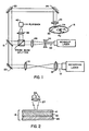
- Figure 1 shows a schematic of an apparatus for writing information on a recording element 16 of the invention and for playing back the recorded information therefrom.
- Recording element 16 comprises, as shown in Figure 2, an overcoat layer such as acrylic 41, a GeTe thin film according to this invention 42 on substrate 45.
- the intensity of a laser diode writing beam 10 is modulated in accordance with information to be recorded on film 42.
- the modulated laser beam 10 is collected by a lens 14 and collimated by a lens 18 and is directed by means of mirror elements 20, 23 and 24 to a high numerical aperture lens 26 which focuses the modulated laser beam to a recording spot 28 on the film 42.
- the first few writing cycles can be used to prepare film 42 for the write-erase cycle, in effect carrying out step b of the method of the invention.
- Preparation of the film for write-erase cycling can also be achieved by other heating techniques. Heating or exposing the film to high power, or short duration light (Zenon) pulses are examples of such techniques. Heating as required in step b.ii. can be carried out on a hot plate, oven or pulsed light exposure.
- Figure 3 is a TEM micrograph of a film which has been prepared for write-erase cycling with laser pulses. Segregation of phases can be inferred by the appearance of regions of two different densities in b) of the micrograph. Selected Area Electron Diffraction (SAED) indicates that the spot is still amorphous, but the region is much easier to crystallize by subsequent laser beams than the unprepared areas. The fact that phase-segregation actually improves the crystallization rate is surprising in view of the teachings of Chen et al.
- the film could have been prepared for write-erasure cycling by heating the film 42 up to its crystallization temperature according to step b.ii. This would bypass initial information of atom phase-segregated amorphous state.
- the entire element 16 is spun at a constant rate, e.g. 1800 rotations per minute (rpm).
- a track of information 30 is recorded on the optical recording layer in the form of selected phase-segregated areas.
- the recording spot 28 is caused (by means not shown) to scan radially inward across the film 42, thereby causing information to be recorded along a spiral or concentric track that extends from an outer radius R O to an inner radius R I .
- the sizes and spacings of the recorded information marks vary in accordance with the information content of the recording laser drive signal, as well as with radial position on film 42.
- Erasure can be accomplished by the above described recording procedure except that the laser 10 is unmodulated, or is modulated at a higher frequency than that carrying the recorded information.
- the element 16, comprising film 42, now bearing the recorded information is spun at the same rate as it was spun during the recording process.
- a laser beam 22 from a readout laser (which can, if desired, be the same laser used for recording) is expanded in diameter by means of lenses 34 and 36.
- the optical path of the readout laser beam is folded by a beam splitter 21 and mirrors 23 and 24 so that the readout laser beam is focused to a playback spot on the film 42 by the high numerical aperture lens 26.
- the film 42 is reflective so that the radiation forming the playback spot is reflected back through the high numerical aperture lens 26 after interacting with the information marks recorded on the film 42.
- a lens 38 directs reflected laser radiation which has been diverted by the prism beamspliter onto a detector 40 which produces an electrical playback signal in response to temporal variations (contrast) in the irradiance of the reflected laser radiation falling on the detector.
- the thin film 42 is written upon with a coherent beam of electromagnetic radiation of sufficient energy to convert selected portions of the film 42 from a crystalline state to the phase-segregated amorphous state.
- the thin film 42 is sufficiently sensitive to laser powers of 2.5 to 20 mW at laser pulsewidth of 50 to 500 ns to make the conversion.
- Test recordings on the thin films were made with a static pit tester.
- the static pit tester provides automated facilities for exposing standard test patterns on two-inch by two-inch glass slides of film samples with a laser.
- the output beam from a 830 nm diode laser is focused onto a spot on the sample through a high NA objective lens.
- the series of laser pulses alternating between a higher power and a lower power is applied to the sample.
- the reflectance of the sample after each laser pulse is measured and recorded to indicate phase changes caused by the preceding laser pulses.
- the higher power pulses bring the material to above the melting point and change the materials from the crystalline state to the phase-segregated amorphous state after cooling.
- the reflectance of the material is decreased.
- the lower power laser pulses heat the material to below the melting point and cause the material to crystallize.
- the reflectance between the two states is referred to as reflectance contrast by the following definition: wherein R c and R x are the reflectances of the crystalline and the amorphous states respectively.
- the reflectance contrast is used to select erasable media and is shown in Figure 4 for the Ge-Te alloys using a particular set of write/erase conditions.
- a Ge-Te alloy thin-film (90 X 10 ⁇ 9m thick) was prepared by co-sputtering from two RF-magnetron targets containing Ge and Te, respectively, using 0.4 Pa (3mTorr) of purified Ar as the sputtering gas.
- the two targets were spaced apart with glass substrates spinning over them at 150 rpm so that alternating thin layers .05 X 10 ⁇ 9m ( ⁇ 0.05 nm) of Ge and Te could be coated from the two targets to form an alloyed thin-film.
- the composition of the film was determined by the relative deposition rates from the two targets. In this example a composition of about Ge 0.59 Te 0.41 was achieved.
- a sprayed clear acrylic layer of several ⁇ m thickness was applied over the surface of the film. This layer was used to reduce the deformation of the Ge-Te thin-film by the write/erase laser beam so that erasable read/write experiments could be performed.
- Figure 3 is a transmission electron micrograph of the a) amorphous as deposited film, b) the phase-segregated amorphous state, and c) the crystallized state of the film.
- the physical state of the film in b) and c) result from the read-write cycling. Writing converts the film from c) to b). Erasure converts the film from b) to c). The results clearly indicate that the film could be written on and then erased over 1000 cycles.
- Each element comprises a GeTe alloy thin film for recording. Each element consisted of a different Ge/Te concentration ratio. Several read-write cycles were carried out on each film as described in example 1. The Ge/Te concentration ratio in the films range from 70/30 to 35/65. Based on the contrast achieved between the amorphous segregated phase (written) and the crystallized phase (erase), concentration ratios of Ge/Te in the range 70/30 to 45/55 proved to be erasable. The reflection contrast achieved with these varying concentration ratios is shown in the Figure 4. The write-erasure time was 0.8 ⁇ s.
- Figure 5 is a reflectance versus temperature graph performed with films containing various concentrations of GeTe.
- the Ge content of each film is indicated on the graph.
- This graph shows the effect of heating on the optical reflectance of GeTe films at various concentrations of Ge.
- the increase in reflectance is caused by the crystallization of the films.
- the temperature at which crystallization takes place also increases so that according to the graph a film comprising 59.1 atom percent of Ge crystallizes at a temperature above 275°C.
- the crystallization temperature of a thin film comprising 49.9 percent Ge is 210°C. This data shows that the films of this invention have long data retention times.
Abstract
Description
- This invention relates to an optical recording method and to optical recording elements used in the method.
- It is known that certain materials, which exist in a stable condition at room temperature, in either a substantially amorphous or substantially crystalline state can be converted from one of these states to the other by supplying sufficient energy to heat the material to its melt temperature and then allowing it to cool under controlled conditions to a crystalline or an amorphous state.
- It is also known that such materials may be used for storing and retrieving information. These materials may be used in the form of thin films for optical recordings. The thin films are written upon by selectively changing particular areas of the thin film from one state to the other (from amorphous to crystalline or crystalline to amorphous). Such change may be accomplished by providing a low amplitude energy pulse for sufficient duration to heat the material to just below its melting point after which the film slowly cools in the crystalline state. On the other hand to convert the film from a crystalline to an amorphous state, rapid cooling is essential. This change, may be accomplished by pulsing the film with a high energy pulse source to raise the film to its melting point. The film must then be rapidly cooled to freeze the film in the amorphous state before crystallization can occur.
- One of the most difficult challenges is to develop optical recording elements which possess both fast erasure speed and long data retention time. Both of these desirable features relate to the transition of the film from the amorphous phase to the crystalline phase. To have fast erasure speed requires the crystallization rate to be exceedingly fast at the elevated temperatures produced by a laser pulse. Long data retention time, on the other hand, requires exceedingly slow crystallization rate during keeping near room temperatures.
- Most studies have been concentrated on films of tellurium rich (Te >85%) alloys. For these materials, however, long erasure time (>1 µs) is needed unless data retention time is sacrificed.
- Recently, Chen et al, in a paper entitled "New Ideas for Phase-Change Media-Achieving Sub-Microsecond Erase With Data Stability", presented October 15-17, 1985, at the Topical Meeting on Optical Data Storage, IEEE and OSA, in Washington, D.C., has reported achieving a significant improvement in performance by using nearly stoichiometric GeTe films. The problem is that such films possess limited corrosion resistance and data stability.
- The objective of this invention is to provide a method of writing and erasing written information on optical recording elements while at the same time avoiding the above prior art problem. The foregoing objective is achieved with the present invention which provides a method comprising the steps of:
- a. providing an optical recording element comprising a support and an amorphous thin film of a GeTe alloy; wherein the ratio of Ge:Te in the film is 45/55 to 70/30 on an atom-to-atom basis
- b. preparing the thin film for writing and erasing cycles by:
- i. heating the film, or a selected portion thereof, above its melting point using a laser or light beam; rapidly cooling the film to form a phase-segregated amorphous state evidenced by the appearance of regions of different densities and then heating the same areas of the film with a focused beam to below its melting point to transform these areas from the phase-segregated amorphous state to a crystalline state; or,
- ii. crystallizing the film, or a selected portion thereof, by heating the film to its crystallization temperature;
- c. writing on selected portions of the thus prepared film with a focused information modulated laser beam, thereby converting those portions on the films upon which the laser beam has been focused to a phase-segregated amorphous state from a crystalline state; and,
- d. when desired, erasing the written information by heating those portions of the film bearing the written information with a focused unmodulated or high frequency modulated laser beam thereby converting the written portions of the film to a crystalline state from the phase-segregated amorphous state.
- The method of this invention makes erasable optical recording elements comprising thin films of GeTe, in which the Ge/Te ratio varies from 45/55 to 70/30. The films possess improved contrast. Moreover, the erasure rate is significantly less than 1 microsecond.
- In preferred embodiments the optical recording elements used in the method of this invention comprise greater than 55 atomic percent of Ge. Such Ge rich films are more desirable than stoichiometric GeTe films in that they exhibit improved corrosion resistance and improved amorphous phase stability compared to stoichiometric GeTe films. Corrosion resistance is improved because the excess Ge reduces the concentration of the corrosion prone Te. Amorphous phase stability is improved because the crystallization temperature of the Ge/Te film increases drastically with increasing Ge. In thin films containing greater than 59 atomic percent Ge, crystallization temperatures are above 275°C. thereby ensuring improved data stability.
- The present invention will now be described by way of example with reference to the accompanying drawings in which:-
- Figure 1 is a description of a schematic recording, readback, and erasure apparatus for use in the method of the invention;
- Figure 2 is a schematic cross section of an optical recording element for use in the method of the invention;
- Figure 3 is a Transmission Electron Micrograph (TEM) of a thin film of the invention in various physical states;
- Figure 4 is a curve showing the experimental results of the Examples 2-29 herein; and
- Figure 5 is a reflectance versus temperature graph.
- Thin amorphous film recording layers can be prepared by conventional thin film deposition techniques such as evaporation, RF (radio frequency) and DC (direct current) sputtering from an alloy target, and RF and DC co-sputtering from targets of the individual elements. Enhancement of sputtering processes by applying magnetic fields (magnetron sputtering) can also be used. The thickness of the films can be from a few tens (10) to a few hundreds nanometers (500 nm) depending on the compromise among factors such as sensitivity, production rate, material cost, ease of control, etc.
- Supports upon which such films are deposited include plastic plates, such as polyethylene terephthalate, polymethyl methacrylate, polycarbonate, glass plates, metal plates or paper.
- Figure 1 shows a schematic of an apparatus for writing information on a
recording element 16 of the invention and for playing back the recorded information therefrom.Recording element 16 comprises, as shown in Figure 2, an overcoat layer such as acrylic 41, a GeTe thin film according to thisinvention 42 onsubstrate 45. In response to a drive signal, the intensity of a laserdiode writing beam 10 is modulated in accordance with information to be recorded onfilm 42. The modulatedlaser beam 10 is collected by alens 14 and collimated by alens 18 and is directed by means ofmirror elements numerical aperture lens 26 which focuses the modulated laser beam to arecording spot 28 on thefilm 42. - The first few writing cycles can be used to prepare
film 42 for the write-erase cycle, in effect carrying out step b of the method of the invention. - Preparation of the film for write-erase cycling can also be achieved by other heating techniques. Heating or exposing the film to high power, or short duration light (Zenon) pulses are examples of such techniques. Heating as required in step b.ii. can be carried out on a hot plate, oven or pulsed light exposure. Figure 3 is a TEM micrograph of a film which has been prepared for write-erase cycling with laser pulses. Segregation of phases can be inferred by the appearance of regions of two different densities in b) of the micrograph. Selected Area Electron Diffraction (SAED) indicates that the spot is still amorphous, but the region is much easier to crystallize by subsequent laser beams than the unprepared areas. The fact that phase-segregation actually improves the crystallization rate is surprising in view of the teachings of Chen et al.
- Of course the film could have been prepared for write-erasure cycling by heating the
film 42 up to its crystallization temperature according to step b.ii. This would bypass initial information of atom phase-segregated amorphous state. - During the write portion of the cycle, the
entire element 16 is spun at a constant rate, e.g. 1800 rotations per minute (rpm). As a result, a track ofinformation 30 is recorded on the optical recording layer in the form of selected phase-segregated areas. As recording continues, therecording spot 28 is caused (by means not shown) to scan radially inward across thefilm 42, thereby causing information to be recorded along a spiral or concentric track that extends from an outer radius RO to an inner radius RI. The sizes and spacings of the recorded information marks vary in accordance with the information content of the recording laser drive signal, as well as with radial position onfilm 42. - Erasure can be accomplished by the above described recording procedure except that the
laser 10 is unmodulated, or is modulated at a higher frequency than that carrying the recorded information. - During the readback process, the
element 16, comprisingfilm 42, now bearing the recorded information is spun at the same rate as it was spun during the recording process. Alaser beam 22 from a readout laser (which can, if desired, be the same laser used for recording) is expanded in diameter by means oflenses beam splitter 21 and mirrors 23 and 24 so that the readout laser beam is focused to a playback spot on thefilm 42 by the highnumerical aperture lens 26. Thefilm 42 is reflective so that the radiation forming the playback spot is reflected back through the highnumerical aperture lens 26 after interacting with the information marks recorded on thefilm 42. Alens 38 directs reflected laser radiation which has been diverted by the prism beamspliter onto adetector 40 which produces an electrical playback signal in response to temporal variations (contrast) in the irradiance of the reflected laser radiation falling on the detector. - The
thin film 42 is written upon with a coherent beam of electromagnetic radiation of sufficient energy to convert selected portions of thefilm 42 from a crystalline state to the phase-segregated amorphous state. Thethin film 42 is sufficiently sensitive to laser powers of 2.5 to 20 mW at laser pulsewidth of 50 to 500 ns to make the conversion. - Test recordings on the thin films were made with a static pit tester. The static pit tester provides automated facilities for exposing standard test patterns on two-inch by two-inch glass slides of film samples with a laser. For the erasability studies, the output beam from a 830 nm diode laser is focused onto a spot on the sample through a high NA objective lens. The series of laser pulses alternating between a higher power and a lower power is applied to the sample. The reflectance of the sample after each laser pulse is measured and recorded to indicate phase changes caused by the preceding laser pulses. The higher power pulses bring the material to above the melting point and change the materials from the crystalline state to the phase-segregated amorphous state after cooling. The reflectance of the material is decreased. The lower power laser pulses heat the material to below the melting point and cause the material to crystallize. The reflectance between the two states is referred to as reflectance contrast by the following definition:

- The practice of the invention is illustrated by the following examples:
- A Ge-Te alloy thin-film (90
X 10⁻⁹m thick) was prepared by co-sputtering from two RF-magnetron targets containing Ge and Te, respectively, using 0.4 Pa (3mTorr) of purified Ar as the sputtering gas. The two targets were spaced apart with glass substrates spinning over them at 150 rpm so that alternating thin layers .05X 10⁻⁹m (<0.05 nm) of Ge and Te could be coated from the two targets to form an alloyed thin-film. The composition of the film was determined by the relative deposition rates from the two targets. In this example a composition of about Ge0.59Te0.41 was achieved. After the deposition, a sprayed clear acrylic layer of several µm thickness was applied over the surface of the film. This layer was used to reduce the deformation of the Ge-Te thin-film by the write/erase laser beam so that erasable read/write experiments could be performed. - Write and erase cycling on the thin film was performed with the static tester described hereinbefore using an 860 nm diode laser beam focused by a 0.95 NA objective lens of variable powers and pulse lengths. Using 800 ns, 3.3 mW pulses for erasing (crystallizing) and 800 ns, 10 mW pulses for writing (amorphizing) the cycling of the material in a spot between the crystalline state and the amorphous state was monitored by the reflectance changes. Over 1000 write-erase cycles were carried on the film, thus this film was erasable over 1000 of such cycles. The first few cycles in this example served to prepare the film for writing and erasure according to step b. of the method of this invention.
- Figure 3 is a transmission electron micrograph of the a) amorphous as deposited film, b) the phase-segregated amorphous state, and c) the crystallized state of the film. The physical state of the film in b) and c) result from the read-write cycling. Writing converts the film from c) to b). Erasure converts the film from b) to c). The results clearly indicate that the film could be written on and then erased over 1000 cycles.
- Twenty-eight (28) different optical recording elements were prepared as in example 1. Each element comprises a GeTe alloy thin film for recording. Each element consisted of a different Ge/Te concentration ratio. Several read-write cycles were carried out on each film as described in example 1. The Ge/Te concentration ratio in the films range from 70/30 to 35/65. Based on the contrast achieved between the amorphous segregated phase (written) and the crystallized phase (erase), concentration ratios of Ge/Te in the range 70/30 to 45/55 proved to be erasable. The reflection contrast achieved with these varying concentration ratios is shown in the Figure 4. The write-erasure time was 0.8 µs.
- Figure 5 is a reflectance versus temperature graph performed with films containing various concentrations of GeTe. The Ge content of each film is indicated on the graph. This graph shows the effect of heating on the optical reflectance of GeTe films at various concentrations of Ge. The increase in reflectance is caused by the crystallization of the films. As the Ge content of the film increases, the temperature at which crystallization takes place also increases so that according to the graph a film comprising 59.1 atom percent of Ge crystallizes at a temperature above 275°C. In comparison, the crystallization temperature of a thin film comprising 49.9 percent Ge is 210°C. This data shows that the films of this invention have long data retention times.
Claims (5)
i. heating the film, or a selected portion thereof, above its melting point using a pulsed laser or light beam; rapidly cooling the film to form a phase-segregated amorphous state evidenced by the appearance of regions of different densities; and then heating the same areas of the film with a focused beam to below its melting point to transform those areas from the phase-segregated amorphous state into a crystalline state; or,
ii. crystallizing the film, or a selected portion thereof, by heating the film to its crystallization temperature;
Applications Claiming Priority (2)
| Application Number | Priority Date | Filing Date | Title |
|---|---|---|---|
| US907553 | 1986-09-15 | ||
| US06/907,553 US4797871A (en) | 1986-09-15 | 1986-09-15 | Erasable optical recording method |
Publications (2)
| Publication Number | Publication Date |
|---|---|
| EP0260921A2 true EP0260921A2 (en) | 1988-03-23 |
| EP0260921A3 EP0260921A3 (en) | 1989-07-26 |
Family
ID=25424296
Family Applications (1)
| Application Number | Title | Priority Date | Filing Date |
|---|---|---|---|
| EP87308122A Withdrawn EP0260921A3 (en) | 1986-09-15 | 1987-09-15 | Erasable optical recording method |
Country Status (4)
| Country | Link |
|---|---|
| US (1) | US4797871A (en) |
| EP (1) | EP0260921A3 (en) |
| JP (1) | JPS63132090A (en) |
| CA (1) | CA1258172A (en) |
Cited By (5)
| Publication number | Priority date | Publication date | Assignee | Title |
|---|---|---|---|---|
| EP0352105A2 (en) * | 1988-07-22 | 1990-01-24 | Fujitsu Limited | Optical disc medium |
| EP0391848A1 (en) * | 1989-04-06 | 1990-10-10 | Ciba-Geigy Ag | Laser lettering of ceramic materials, glazes, glass ceramics and glasses |
| EP0405605A2 (en) * | 1989-06-30 | 1991-01-02 | Fuji Xerox Co., Ltd. | Optical recording process |
| EP0416431A2 (en) * | 1989-09-07 | 1991-03-13 | BASF Aktiengesellschaft | Recording medium for reversible optical recording as well as a reproducing method using this recording medium |
| EP0971342A1 (en) * | 1997-03-27 | 2000-01-12 | Matsushita Electric Industrial Co., Ltd. | Recording and reproducing method for optical information recording medium and optical information recording medium |
Families Citing this family (6)
| Publication number | Priority date | Publication date | Assignee | Title |
|---|---|---|---|---|
| US5056079A (en) * | 1988-08-04 | 1991-10-08 | Literal Corporation | Multi-state optical contrasts in optical recording media for data compression |
| JPH02301019A (en) * | 1989-05-15 | 1990-12-13 | Nhk Spring Co Ltd | Optical recorder |
| US5294518A (en) * | 1992-05-01 | 1994-03-15 | International Business Machines Corporation | Amorphous write-read optical storage memory |
| TWI246681B (en) * | 2000-12-15 | 2006-01-01 | Koninkl Philips Electronics Nv | Optical information medium and its use |
| CN107475644B (en) * | 2017-08-07 | 2019-09-24 | 南方科技大学 | A kind of method of determining alloy material amorphous formation ability and the device used |
| CN107283047B (en) * | 2017-08-07 | 2020-04-14 | 南方科技大学 | Device and method for preparing amorphous alloy by using pulse laser and application |
Citations (5)
| Publication number | Priority date | Publication date | Assignee | Title |
|---|---|---|---|---|
| DE2309106B2 (en) * | 1972-04-20 | 1975-05-22 | International Business Machines Corp., Armonk, N.Y. (V.St.A.) | Method for optical information storage and device for carrying out the method |
| FR2420188A1 (en) * | 1978-03-16 | 1979-10-12 | Labo Electronique Physique | Recording device for optical information - comprises material sensitive to radiation of below 1.2 microns wavelength on a support |
| EP0180103A2 (en) * | 1984-11-01 | 1986-05-07 | Energy Conversion Devices, Inc. | Method of forming an optical data storage device and the optical data storage device formed thereby |
| EP0182153A2 (en) * | 1984-11-21 | 1986-05-28 | Energy Conversion Devices, Inc. | Data storage device using phase changeable material |
| EP0212336A1 (en) * | 1985-08-15 | 1987-03-04 | International Business Machines Corporation | A method of optical recording |
Family Cites Families (2)
| Publication number | Priority date | Publication date | Assignee | Title |
|---|---|---|---|---|
| JPS5331106A (en) * | 1976-09-03 | 1978-03-24 | Hitachi Ltd | Information recording member |
| JPS5968844A (en) * | 1982-10-14 | 1984-04-18 | Matsushita Electric Ind Co Ltd | Optical reversible recording and reproducing device |
-
1986
- 1986-09-15 US US06/907,553 patent/US4797871A/en not_active Expired - Lifetime
- 1986-11-24 CA CA000523610A patent/CA1258172A/en not_active Expired
-
1987
- 1987-09-14 JP JP62228661A patent/JPS63132090A/en active Pending
- 1987-09-15 EP EP87308122A patent/EP0260921A3/en not_active Withdrawn
Patent Citations (5)
| Publication number | Priority date | Publication date | Assignee | Title |
|---|---|---|---|---|
| DE2309106B2 (en) * | 1972-04-20 | 1975-05-22 | International Business Machines Corp., Armonk, N.Y. (V.St.A.) | Method for optical information storage and device for carrying out the method |
| FR2420188A1 (en) * | 1978-03-16 | 1979-10-12 | Labo Electronique Physique | Recording device for optical information - comprises material sensitive to radiation of below 1.2 microns wavelength on a support |
| EP0180103A2 (en) * | 1984-11-01 | 1986-05-07 | Energy Conversion Devices, Inc. | Method of forming an optical data storage device and the optical data storage device formed thereby |
| EP0182153A2 (en) * | 1984-11-21 | 1986-05-28 | Energy Conversion Devices, Inc. | Data storage device using phase changeable material |
| EP0212336A1 (en) * | 1985-08-15 | 1987-03-04 | International Business Machines Corporation | A method of optical recording |
Cited By (11)
| Publication number | Priority date | Publication date | Assignee | Title |
|---|---|---|---|---|
| EP0352105A2 (en) * | 1988-07-22 | 1990-01-24 | Fujitsu Limited | Optical disc medium |
| EP0352105A3 (en) * | 1988-07-22 | 1990-11-28 | Fujitsu Limited | Optical disc medium |
| US5144618A (en) * | 1988-07-22 | 1992-09-01 | Fujitsu Limited | Optical disc medium |
| EP0391848A1 (en) * | 1989-04-06 | 1990-10-10 | Ciba-Geigy Ag | Laser lettering of ceramic materials, glazes, glass ceramics and glasses |
| EP0405605A2 (en) * | 1989-06-30 | 1991-01-02 | Fuji Xerox Co., Ltd. | Optical recording process |
| EP0405605A3 (en) * | 1989-06-30 | 1992-08-05 | Fuji Xerox Co., Ltd. | Optical recording process |
| US6114087A (en) * | 1989-06-30 | 2000-09-05 | Fuji Xerox Co., Ltd. | Optical recording medium |
| EP0416431A2 (en) * | 1989-09-07 | 1991-03-13 | BASF Aktiengesellschaft | Recording medium for reversible optical recording as well as a reproducing method using this recording medium |
| EP0416431A3 (en) * | 1989-09-07 | 1992-01-22 | Basf Aktiengesellschaft | Recording medium for reversible optical recording as well as a reproducing method using this recording medium |
| EP0971342A1 (en) * | 1997-03-27 | 2000-01-12 | Matsushita Electric Industrial Co., Ltd. | Recording and reproducing method for optical information recording medium and optical information recording medium |
| EP0971342A4 (en) * | 1997-03-27 | 2006-03-29 | Matsushita Electric Ind Co Ltd | Recording and reproducing method for optical information recording medium and optical information recording medium |
Also Published As
| Publication number | Publication date |
|---|---|
| JPS63132090A (en) | 1988-06-04 |
| CA1258172A (en) | 1989-08-08 |
| US4797871A (en) | 1989-01-10 |
| EP0260921A3 (en) | 1989-07-26 |
Similar Documents
| Publication | Publication Date | Title |
|---|---|---|
| US4798785A (en) | Recording elements comprising write-once thin film alloy layers | |
| US4960680A (en) | Recording elements comprising write-once thin film alloy layers | |
| EP0260920B1 (en) | Thin film amorphous optical recording films | |
| US4774170A (en) | Recording elements comprising write-once thin film alloy layers | |
| US4795695A (en) | Recording elements comprising write-once thin film alloy layers | |
| US5637371A (en) | Phase change optical recording medium and activation energy determining method | |
| EP1030292B1 (en) | Optical recording medium and method for its initialization | |
| US4812386A (en) | Recording elements comprising write-once thin film alloy layers | |
| CA1258172A (en) | Erasable optical recording method | |
| US4981772A (en) | Optical recording materials comprising antimony-tin alloys including a third element | |
| JPH0288288A (en) | Optical recording material composed of antimony-tin alloy containing third element | |
| EP0278789B1 (en) | Recording elements comprising write-once thin film alloy layers | |
| US4812385A (en) | Recording elements comprising write-once thin film alloy layers | |
| US4865955A (en) | Recording elements comprising write-once thin film alloy layers | |
| US5055331A (en) | Phase-change optical recording media | |
| US5015548A (en) | Erasable phase change optical recording elements and methods | |
| US5196294A (en) | Erasable optical recording materials and methods based on tellurium alloys | |
| JP2726259B2 (en) | Information recording method | |
| Ishigaki et al. | New erasable optical media using Sb-Se-Bi alloy film | |
| JP2537875B2 (en) | Information recording method | |
| JPH01191344A (en) | Optical information recording medium | |
| WO1990007181A1 (en) | Erasable phase change optical recording elements and methods | |
| JPS63153737A (en) | Optical recording medium |
Legal Events
| Date | Code | Title | Description |
|---|---|---|---|
| PUAI | Public reference made under article 153(3) epc to a published international application that has entered the european phase |
Free format text: ORIGINAL CODE: 0009012 |
|
| AK | Designated contracting states |
Kind code of ref document: A2 Designated state(s): DE FR GB NL |
|
| PUAL | Search report despatched |
Free format text: ORIGINAL CODE: 0009013 |
|
| AK | Designated contracting states |
Kind code of ref document: A3 Designated state(s): DE FR GB NL |
|
| 17P | Request for examination filed |
Effective date: 19890831 |
|
| 17Q | First examination report despatched |
Effective date: 19901227 |
|
| STAA | Information on the status of an ep patent application or granted ep patent |
Free format text: STATUS: THE APPLICATION IS DEEMED TO BE WITHDRAWN |
|
| 18D | Application deemed to be withdrawn |
Effective date: 19910507 |
|
| RIN1 | Information on inventor provided before grant (corrected) |
Inventor name: PAN, KEE-CHUANC/O EASTMAN KODAK COMPANY Inventor name: VAZAN, FRIDRICHC/O EASTMAN KODAK COMPANY Inventor name: TYAN, YUAN SHENGC/O EASTMAN KODAK COMPANY |