EP0257526B1 - Amplitude equalizer - Google Patents
Amplitude equalizer Download PDFInfo
- Publication number
- EP0257526B1 EP0257526B1 EP87111977A EP87111977A EP0257526B1 EP 0257526 B1 EP0257526 B1 EP 0257526B1 EP 87111977 A EP87111977 A EP 87111977A EP 87111977 A EP87111977 A EP 87111977A EP 0257526 B1 EP0257526 B1 EP 0257526B1
- Authority
- EP
- European Patent Office
- Prior art keywords
- circuit
- amplitude
- frequency
- path
- characteristic
- Prior art date
- Legal status (The legal status is an assumption and is not a legal conclusion. Google has not performed a legal analysis and makes no representation as to the accuracy of the status listed.)
- Expired - Lifetime
Links
Images


Classifications
-
- H—ELECTRICITY
- H04—ELECTRIC COMMUNICATION TECHNIQUE
- H04B—TRANSMISSION
- H04B3/00—Line transmission systems
- H04B3/02—Details
- H04B3/04—Control of transmission; Equalising
- H04B3/14—Control of transmission; Equalising characterised by the equalising network used
- H04B3/143—Control of transmission; Equalising characterised by the equalising network used using amplitude-frequency equalisers
- H04B3/145—Control of transmission; Equalising characterised by the equalising network used using amplitude-frequency equalisers variable equalisers
Definitions
- the present invention relates to an amplitude equalizer, more particularly, to an amplitude equalizer able to produce an output having a flat delay-frequency characteristic and a powerful amplitude-frequency characteristic.
- the amplitude equalizer of the present invention is useful as an equalizer for equalizing, in particular, the first order slope in amplitude distortion due to the above-mentioned multi-path fading.
- amplitude equalizers are those comprised of constant resistor networks using only passive elements such as capacitors (C), inductors (L), and resistors (R), resonant automatic equalizers which equalize an input signal in a frequency domain using a frequency-amplitude characteristic reverse to the frequency-amplitude characteristic of the input signal, and transversal filter type automatic equalizers which equalize in time domains.
- passive elements such as capacitors (C), inductors (L), and resistors (R)
- resonant automatic equalizers which equalize an input signal in a frequency domain using a frequency-amplitude characteristic reverse to the frequency-amplitude characteristic of the input signal
- transversal filter type automatic equalizers which equalize in time domains.
- Resonant automatic equalizers apply a variable resonator to the input signal subject to selective fading to detect the frequency in the frequency-amplitude characteristic of the input signal and detect the equalization residual in the spectrum of the equalized output signal.
- an equalized signal is obtained as the output of the variable resonator.
- An amplitude equalizer using such a resonator is proposed, for example, in Japanese Unexamined Patent Publication (Kokai) No. 60-64515 (published on April 13, 1985).
- Amplitude equalizers using transversal filters multiply the tap outputs of delay circuits provided with taps by various tap coefficients and sum up the results of the calculations as an output. By varying the tap coefficients in accordance with an error signal obtained by discrimination of the level of the summed output, the error signal is controlled to zero and the output equalized.
- amplitude equalizers those comprised of constant resistor networks feature a weak resultant frequency-amplitude characteristic and have to be arranged in multi-stage constructions to obtain a powerful amplitude equalization characteristic. This complicates the circuit construction and complicates the design procedure.
- resonant automatic equalizers can equalize the amplitude-frequency characteristic and delay-frequency characteristic when the interference wave is small with respect to the level of the direct wave.
- the delay-frequency characteristic is inverted, which works with the delay-frequency characteristic due to the resonance circuit to conversely deteriorate the delay-frequency characteristic of the output.
- An amplitude equalizer using a transversal filter can equalize signals subjected to selective fading in the case of an interference wave larger than the level of the direct wave, but the first order component of the amplitude-frequency characteristic in the demodulator is poor, the full equalization capability cannot be exhibited.
- resonant automatic equalizers and transversal automatic equalizers feature complicated detection circuitry and control circuitry, resulting in not only a tendency to larger circuit sizes but also considerably difficult design procedures.
- the present invention has as its object the provision of an amplitude equalizer which can equalize the first order slope using a simple construction and has as its further object the provision of an automatic amplitude equalizer which can automatically equalize the first order slope with such a simple construction.
- the present invention features the summing of the outputs of two circuit means having opposite characteristics so as to enable equalization of the first order slope and further the addition of a feedback means to enable automatic amplitude equalization.
- the above-mentioned circuit means having opposing characteristics are preferably a minimum phase circuit and non-minimum phase circuit.
- the two circuit means having opposing characteristics use is made, as the two circuit means having opposing characteristics, of generally a positive slope first order amplitude equalizer and a negative slope first order amplitude equalizer.
- these positive and negative slope first order amplitude equalizers are comprised of the above-mentioned minimum and non-minimum phase circuits.
- the above-mentioned feedback means use is made of a first order amplitude equalization residual detection circuit.
- Figure 1 is a schematic block diagram of an amplitude equalizer. As shown in the figure, it is constituted by a minimum phase circuit 1 and a non-minimum phase circuit 2 connected in series.
- the minimum phase circuit 1 emits as an output through a combiner 13 a combination of one of the signals of an input signal S in branched into two ways and a signal consisting of the other signal delayed by a delay element 11 and attenuated by an attenuator 12.
- the non-minimum phase circuit 2 emits as an output through a combiner 16 a combination of a signal consisting of one of the signals of an input signal S ⁇ in branched into two ways, attenuated by an attenuator 14, and a signal consisting of the other signal delayed by a delay element 15. Note that circuits 1 and 2 may be connected in this order or may be connected in a reverse order.
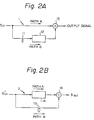
- Figures 2A and 2B show the equivalent circuit of the minimum phase circuit and the non-minimum phase circuit.
- the minimum phase circuit 1 as shown in Fig. 2A, branches an input signal into path A and path B, inserts the delay element 11 and attenuator 12 in the signal of path B, and combines the signal of path A and the signal of path B in the combiner 13 for an output.
- the non-minimum phase circuit 2 as shown in Fig. 2B, branches the input signal into path A and path B, inserts an attenuator in path A and inserts a delay element 15 in path B, and combines the signal of path A and the signal of path B in the combiner 16 for an output.
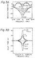
- the delay-frequency characteristic in the case of ⁇ ⁇ 1 in Fig. 2A is reverse from the delay-frequency characteristic in the case of ⁇ > 1 shown in Fig. 2B. Therefore, by connecting in series the circuit of Fig. 2A and the circuit of Fig. 2B, the delay-frequency characteristic in the output is cancelled out and the characteristic becomes flat. Only the amplitude characteristic is added on.
- ⁇ , ⁇ , and the phases of the paths are set appropriately to obtain the reverse characteristic from the characteristic to be equalized, thus obtaining an amplitude equalizer having the desired equalization characteristic.
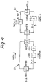
- Figure 4 shows an example of an amplitude equalizer according to the present invention, wherein HYB 1 to HYB 4 are hybrid circuits, DL 1 and DL 2 are delay lines, ATT 1 and ATT 2 are attenuators, and PS 1 and PS 2 are phase shifters.
- an input signal S in is connected to the input side of the hybrid circuit HYB 1.
- One of the output sides of the hybrid circuit HYB 1 is connected in series to one of the input sides of the hybrid circuit HYB 2, while the other output side of the hybrid circuit HYB 1 is connected in series through the delay line DL 1 and the attenuator 1 and phase shifter 1 to the other input side of the hybrid circuit HYB 2.
- the output side of the hybrid circuit HYB 2 is connected to the input side of the hybrid circuit HYB 3.
- One of the output sides of the hybrid circuit HYB 3 is connected via the attenuator ATT 2 to one of the input sides of the hybrid circuit HYB 4, while the other output side of the hybrid circuit HYB 3 is connected in series via the delay line DL 2 and the phase shifter PS 2 to the other input side of the hybrid circuit HYB 4.
- the input signal S in is split to the path A and path B in the hybrid circuit HYB 1.
- the signal of path A is input directly to the hybrid circuit HYB 2, while the signal of path B is delayed by the delay line DL 1, attenuated by the attenuator ATT 1, shifted in phase in the phase shifter PS 1, and then input to the hybrid circuit HYB 2.
- the hybrid circuit HYB 2 combines the two path signals.
- the output signal of the hybrid circuit HYB 2 is split to the path C and path D in the hybrid circuit HYB 3.
- the signal of path C is attenuated by the attenuator ATT 2, then input to the hybrid circuit HYB 4, while the signal of path D is delayed by the delay line DL 2, shifted in phase by the phase shifter PS 2, and then input to the hybrid circuit HYB 4.
- the hybrid circuit HYB 4 combines the two path signals.
- the circuit 21 located between the hybrid circuit HYB 1 and the hybrid circuit HYB 2 comprises the minimum phase circuit.
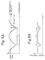
- Figure 5 shows the frequency characteristics of the minimum phase circuit, Fig. 5A showing the frequency-amplitude characteristic and Fig. 5B showing the delay-frequency characteristic.
- the interval between two notch frequencies appearing in the frequency characteristics is 1/ ⁇ and is determined by the delay time difference with the path A arising from the delay line DL 1 provided in path B.
- the position of the notches can be arbitrarily set by changing the phase of the path B. That is, when desiring to change just the position of the notches without changing the interval of the notches, one need only set the phase shift amount of the phase shifter PS 1 to a suitable value.
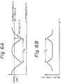
- FIG. 6 shows the frequency characteristics of the non-minimum phase circuit 22, Fig. 6A showing the frequency-amplitude characteristic and Fig. 6B the delay-frequency characteristic.
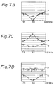
- Figure 7 shows an example of the design of an amplitude equalizer.
- the illustrated values are given to the attenuators ATT 1 and ATT 2 and in-phase hybrid circuits are used for the hybrid circuit HYB 1 to hybrid circuit HYB 4
- the frequency characteristics of the minimum phase circuit 21 and the frequency characteristics of the non-minimum phase circuit 22 becomes as shown by Figs. 7B and C.
- the frequency characteristics of the circuit of Fig. 7A comprising these connected in series become as shown in Fig. 7D.
- the abscissas indicate the frequency and the ordinates indicate the delay-frequency characteristic P (5 nsec/div) and the frequency-amplitude characteristic Q (5 dB/div).
- the output of the circuit of Fig. 7A is flat in its delay-frequency characteristic and augmented in its frequency-amplitude characteristic.
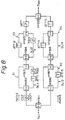
- Figure 8 shows an example of the application of this circuit, illustrating the use as a variable first order amplitude equalizer.
- HYB 11 to HYB 20 indicate hybrid circuits, DL 11 to DL 14 delay lines, ATT 11 to ATT 15 attenuators, PS 11 to PS 13 phase shifters, and VATT a variable attenuator.
- the portions located between the hybrid circuit HYB 12 and HYB 13 and between the hybrid circuit HYB 16 and HYB 17 constitute the minimum phase circuits 31 and 32, while the portions located between the hybrid circuit HYB 14 and HYB 15 and the hybrid circuit HYB 18 and HYB 19 constitute the non-minimum phase circuits 33 and 34.
- the circuit of Fig. 8 comprises amplitude equalizers shown in Fig.
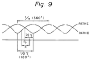
- the interval between the notch frequency of the path I comprised of the minimum phase circuit 31 and the non-minimum phase circuit 33 and the notch of the path II comprised of the minimum phase circuit 32 and the non-minimum phase circuit 34 is selected to be 1/2 ⁇ by the phase-shifters PS 12 and PS 13 within the path I, as shown by Fig. 9.
- a certain range X centered on the intersecting frequency F0 of the two characteristics is used as the transmission band. Therefore, there is a relative phase difference of 180° between the signal of path I and the signal of path II.
- variable attenuator VATT may be of any type so long as it can be varied in its attenuation level. Also, it may be inserted into either the path I or path II or may be inserted in both paths.
- Figures 10A to F and 11A to C show specific examples of the characteristics of the variable first order amplitude equalizer of Fig. 8. These show the delay-frequency characteristic P (ordinate, 5 nsec/div) and the frequency-amplitude characteristic Q (ordinate, 5 dB/div) of various parts, with the frequency as the abscissa, when the notch frequencies of the minimum phase circuits 31 and 32 in the circuit of Fig. 8 are set to 47 MHz and 93 MHz, respectively, and the notch frequencies of the non-minimum phase circuits 33 and 34 are made 47 MHz and 93 MHz, respectively.
- Figure 10A shows the characteristic of the minimum phase circuit 31, Fig. 10D the characteristic of the minimum phase circuit 32, Fig.
- Fig. 10B the characteristic of the non-minimum phase circuit 33
- Fig. 10E the characteristic of the non-minimum phase circuit 34
- Fig. 10C the characteristic of the path I comprised of the minimum phase circuit 31 and the non-minimum phase circuit 33 connected in series
- Fig. 10F the characteristic of the path II comprised of the minimum phase circuit 32 and the non-minimum phase circuit 34 connected in series
- Figs. 11A, 11B, and 11C the characteristics of variable first order amplitude equalizer of Fig. 8 as a whole with path I and path II connected in parallel.
- the characteristics of the path I are a combination of the characteristics of the minimum phase circuit and the non-minimum phase circuit 33.
- the delay-frequency characteristic is flat, and the frequency-amplitude characteristic is augmented.
- the characteristics of the path II are a combination of the characteristics of the minimum phase circuit 32 and the non-minimum phase circuit 34, with the delay-frequency characteristic being flat and the frequency-amplitude characteristic being augmented.
- a combination of the outputs of the two paths is obtained as the output of the hybrid circuit HYB 20. At this time, three types of characteristics are obtained depending on the magnitude of the attenuation by the variable attenuator VATT.
- Figures 11A and 11C show the characteristics of the overall circuit of Fig. 8 in the case of the attenuation of the variable attenuator VATT being smaller and larger than the attenuation of the attenuator ATT 15.
- the delay-frequency characteristics are flat, while the frequency-amplitude characteristics become a negative first order slope and a positive first order slope, respectively.
- Figure 11B shows the characteristics of the overall circuit of Fig. 8 in the case where the attenuation of the variable attenuator VATT and the attenuation of the attenuator ATT 15 are equal. Both the delay-frequency characteristic and the frequency-amplitude characteristic are flat.
- the center frequency f0 of the band in this case is the center frequency of the 47 MHz notch frequency of the path I and the 93 MHz notch frequency of the path II, that is, 70 MHz.
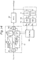
- FIG. 12 is a view of the constitution of an automatic amplitude equalizer based on the circuit of Fig. 8.
- a feedback means 41 is introduced into the circuit of Fig. 8 so as to change the amount of attenuation of the variable attenuator VATT in accordance with the equalization residual in the output signal.
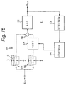
- Figure 13 is a view of a specific constitution of the automatic amplitude equalizer of Fig. 12.
- a variable amplitude equalization circuit corresponding to the circuit of Fig. 8 is indicated by 51 and is shown generally. It is specifically constituted by a negative slope first order amplitude equalizer 56 (corresponding to 31 and 33 in Fig. 12), a positive slope first order amplitude equalizer 55 (corresponding to 32 and 34 in Fig. 12), a variable attenuator 57 (corresponding to VATT in Fig. 12), and a combining circuit 58 (corresponding to HYB 20 in Fig. 12).
- the feedback means 41 of Fig. 12 comprises an automatic gain control (AGC) amplifier 52, a detection circuit 53, and a control circuit 54.
- AGC automatic gain control
- the circuit is comprised of an automatic gain control amplifier 52 for making constant the output signal of a variable amplitude equalization circuit 51, a detection circuit 53 for detecting the first order amplitude equalization residual of the frequency-amplitude characteristic of the output signal of the automatic gain control amplifier 52 using a narrow band filter, detector, etc., and a control circuit 54 for controlling the variable amplitude equalization circuit 51 based on the detected output signal of the detection circuit 53.
- the variable amplitude equalization circuit 51 has a variable attenuator 57 for adjusting the output signal level of either one of the positive slope first order amplitude equalizer 55 and the negative slope first order amplitude equalizer 56.
- the variable attenuator 57 is controlled by the above-mentioned control circuit 54. Signals are combined by a combining circuit 58 for output.
- the automatic gain control amplifier 52 amplifies the signal to a certain level and outputs the result.
- the first order amplitude equalization residual is detected by the detection circuit 53, and, based on the detected output signal, the variable attenuator 57 of the variable amplitude equalization circuit 51 is controlled by the control circuit 54.
- the variable amplitude equalization circuit 51 the output signal levels of the amplitude equalizers 55 and 56 of the positive slope and negative slope are adjusted and the vector-added, so when the two have opposite frequency-amplitude characteristics, the vector-addition results in a flat frequency-amplitude characteristic. If the amount of attenuation of the variable attenuator 57 is made larger, the frequency-amplitude characteristic of the other output signal becomes the characteristic of the combined output signal.
- variable attenuator 57 for a minimum first order amplitude residual, the first order component of the frequency-amplitude characteristic due to the fading can be equalized without deterioration of the group delay-frequency characteristic. Further, the control circuitry controls a single variable attenuator 57 through detection of the first order component, so becomes simple in construction.
- FIG. 14 is a somewhat more concrete view of the automatic amplitude equalizer of Fig. 13.
- 61 indicates a variable amplitude equalization circuit
- 62 an automatic gain control amplifier
- 63 a detection circuit
- 64 a control circuit
- 66 a positive slope first order amplitude equalizer
- 67 a negative slope first order amplitude equalizer
- 68 a fixed attenuator
- 69 a variable attenuator
- 71 and 72 narrow band filters and 73 and 74 detectors.
- the signal received through a digital radio transmission line is converted in frequency to become an intermediate frequency (IF) signal and input to the variable amplitude equalization circuit 61.
- the input signal is branched into two by the hybrid circuit 65 and supplied to the positive slope first order amplitude equalizer 66 and the negative slope first order amplitude equalizer 67.
- the output signal of the positive slope first order amplitude equalizer 66 is applied to the fixed attenuator 68 and the output signal of the negative slope first order amplitude equalizer 67 is applied to the variable attenuator 69.
- the output signals of the fixed attenuator 68 and the variable attenuator 69 are applied to the hybrid circuit 70 and vector added.
- variable attenuator 69 for example, PIN diode
- control circuit 64 by controlling the variable attenuator 69 (for example, PIN diode) by the control circuit 64, it is possible to obtain a desired negative first order slope characteristic as the combined output characteristic, so it is possible to compensate for the first order component of the frequency-amplitude characteristic of the input signal.
- the output signal of the variable amplitude equalization circuit 61 is amplified so as to become fixed in level by the automatic gain control amplifier 62.
- the first order amplitude equalization residual is detected by the detection circuit 63 from the output signal of the automatic gain control amplifier 62.
- different frequency components are extracted by the band filters 71 and 72, detected by the detectors 73 and 74, and supplied to the control circuit 64.
- the levels of the output signals detected by the detectors 73 and 74 are compared and the variable attenuator 69 is controlled in accordance with the first order amplitude equalization residual. For example, when the detected output signal levels are equal, the amount of attenuation of the variable attenuator 19 is controlled to be the same as the attenuation of the fixed attenuator 68.
- Vector addition of the characteristics of the positive slope first order amplitude equalizer 66 and the negative slope first order amplitude equalizer 67 gives a flat frequency-amplitude characteristic.
- the first order amplitude equalization residual exhibits a positive slope first order amplitude characteristic, so control is effected to reduce the attenuation of the variable attenuator 69.
- the variable amplitude equalization circuit 61 is made to exhibit a negative slope frequency-amplitude characteristic, and it is possible to equalize the frequency-amplitude characteristic resulting from the fading.
- the output signal of the negative slope first order amplitude equalizer 67 was added to the variable attenuator 69, but it is also possible to structure things so that the output signal of the positive slope first order amplitude equalizer 66 is applied to the variable attenuator 69 and the output signal of the negative slope first order amplitude equalizer 67 is applied to the fixed attenuator 68. Further, it is possible to make both the two attenuators (68 and 69) variable. Still further, while it is advantageous to use equalizing circuits of the structure of Fig.
- FIG. 4 shows another embodiment of the variable amplitude equalization circuit of Fig. 13, wherein general L-R-C type circuits are used for the equalizers 55 and 56.
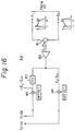
- Figures 16 shows an example of the control circuit of Fig. 14.
- the low frequency (L) side output E L and high frequency (H) side output E H output from the detection circuit 63 are input to a subtractor 81 and the level difference E L - E H of the two is calculated. If E L - E H > 0 , a negative slope characteristic appears. If E L - E H ⁇ 0 , a positive slope characteristic appears.
- the level difference E L - E H is amplified by an amplifier 82, then becomes the control input of the variable attenuator 69 (Fig. 14). If the attenuator 68 (Fig.
- the 14) is also comprised of a variable attenuator, the polarity of the above-mentioned level difference is inverted by an inverter (INV) 83 to give -(E L - E H ). This is used as the control input for the attenuator 68.
- the adders 84 and 85 add an offset DC voltage to E L - E H and -(E L - E H ). This sets the gain of the attenuator to the optimum reference value. It is possible to perform equalization by just the gain control of the attenuator 68, but if the gains of both the attenuators 68 and 69 are controlled, it is possible to perform the wide range equalization.
- an amplitude equalizer is realized which can flatten the delay-frequency characteristic through addition of the outputs of two circuit means having opposite characteristics and can produce a strong frequency-amplitude characteristic. If such equalizer amplitudes are connected in parallel, a variable amplitude equalizer can be realized. In this case, level adjustment is performed on the positive slope and/or negative slope first order amplitude equalizer side. If this level adjustment is performed in accordance with the magnitude of the equalization residual appearing in the output signals, an automatic amplitude equalizer can be realized.
- Each of the above-mentioned amplitude equalizer, the variable amplitude equalizer, and the automatic amplitude equalizer can be realized with a simple construction.
Landscapes
- Engineering & Computer Science (AREA)
- Computer Networks & Wireless Communication (AREA)
- Signal Processing (AREA)
- Cable Transmission Systems, Equalization Of Radio And Reduction Of Echo (AREA)
Description
- The present invention relates to an amplitude equalizer, more particularly, to an amplitude equalizer able to produce an output having a flat delay-frequency characteristic and a powerful amplitude-frequency characteristic.
- In the field of radio communications, particularly the field of digital microwave communications, frequency selective transmission distortion occurs due to multi-path fading. This is a major cause behind deterioration of the communication quality. This transmission distortion reaches as much as tens of decibels when it is extremely large, making difficult equalization by amplitude equalizers with weak amplitude equalization characteristics, such as used in the prior art, and, further, making adaptive equalization difficult. Therefore, demand has arisen for an amplitude equalizer which offers strong amplitude equalization characteristics and which can be easily used for adaptive equalization.
- The amplitude equalizer of the present invention is useful as an equalizer for equalizing, in particular, the first order slope in amplitude distortion due to the above-mentioned multi-path fading.
- Known in the prior art as amplitude equalizers are those comprised of constant resistor networks using only passive elements such as capacitors (C), inductors (L), and resistors (R), resonant automatic equalizers which equalize an input signal in a frequency domain using a frequency-amplitude characteristic reverse to the frequency-amplitude characteristic of the input signal, and transversal filter type automatic equalizers which equalize in time domains.
- Resonant automatic equalizers apply a variable resonator to the input signal subject to selective fading to detect the frequency in the frequency-amplitude characteristic of the input signal and detect the equalization residual in the spectrum of the equalized output signal. By control of the notch frequency which is detected and the resonant frequency of the variable resonator to match each other and by control of the quality factor of the variable resonator for a minimal equalization residual, an equalized signal is obtained as the output of the variable resonator. An amplitude equalizer using such a resonator is proposed, for example, in Japanese Unexamined Patent Publication (Kokai) No. 60-64515 (published on April 13, 1985).
- Amplitude equalizers using transversal filters multiply the tap outputs of delay circuits provided with taps by various tap coefficients and sum up the results of the calculations as an output. By varying the tap coefficients in accordance with an error signal obtained by discrimination of the level of the summed output, the error signal is controlled to zero and the output equalized.
- Of the prior art amplitude equalizers, those comprised of constant resistor networks feature a weak resultant frequency-amplitude characteristic and have to be arranged in multi-stage constructions to obtain a powerful amplitude equalization characteristic. This complicates the circuit construction and complicates the design procedure.
- In the case of approximating the frequency-amplitude characteristic due to fading by a two-wave model of a direct wave and an interference wave having a time delay relative to the same, resonant automatic equalizers can equalize the amplitude-frequency characteristic and delay-frequency characteristic when the interference wave is small with respect to the level of the direct wave. However, when the interference wave is large compared with the level of the direct wave, while it is possible to equalize the frequency-amplitude characteristic, the delay-frequency characteristic is inverted, which works with the delay-frequency characteristic due to the resonance circuit to conversely deteriorate the delay-frequency characteristic of the output.
- An amplitude equalizer using a transversal filter can equalize signals subjected to selective fading in the case of an interference wave larger than the level of the direct wave, but the first order component of the amplitude-frequency characteristic in the demodulator is poor, the full equalization capability cannot be exhibited.
- Further, resonant automatic equalizers and transversal automatic equalizers feature complicated detection circuitry and control circuitry, resulting in not only a tendency to larger circuit sizes but also considerably difficult design procedures.
- The present invention has as its object the provision of an amplitude equalizer which can equalize the first order slope using a simple construction and has as its further object the provision of an automatic amplitude equalizer which can automatically equalize the first order slope with such a simple construction.
- One such equalizer is described in prior art document EP-A-0048646.
- To achieve the above-mentioned objects, the present invention features the summing of the outputs of two circuit means having opposite characteristics so as to enable equalization of the first order slope and further the addition of a feedback means to enable automatic amplitude equalization. Here, the above-mentioned circuit means having opposing characteristics are preferably a minimum phase circuit and non-minimum phase circuit. In the case of the above-mentioned automatic amplitude equalizer, use is made, as the two circuit means having opposing characteristics, of generally a positive slope first order amplitude equalizer and a negative slope first order amplitude equalizer. As the best mode, these positive and negative slope first order amplitude equalizers are comprised of the above-mentioned minimum and non-minimum phase circuits. Note that, as the above-mentioned feedback means, use is made of a first order amplitude equalization residual detection circuit.
- The above-mentioned objects and features of the present invention will become clearer from the following explanation, made in reference to the attached drawings, in which:
- Fig. 1 is a schematic block diagram of the amplitude equalizer of the present invention;
- Fig. 2A is a equivalent circuit of the minimum phase circuit;
- Fig. 2B is a equivalent circuit diagram of the non-minimum phase circuit;
- Fig. 3A is a graph of the amplitude-frequency characteristics of the circuits of Fig. 2A and Fig. 2B;
- Fig. 3B is a graph of the delay-frequency characteristics of the circuits of Fig. 2A and Fig. 2B;
- Fig. 4 is a circuit block diagram of an amplitude equalizer according to the present invention;
- Fig. 5A is a graph of the amplitude-frequency characteristic of the minimum phase circuit;
- Fig. 5B is a graph of the delay-frequency characteristic of the minimum phase circuit;
- Fig. 6A is a graph of the amplitude-frequency characteristic of the non-minimum phase circuit;
- Fig. 6B is a graph of the delay-frequency characteristic of the non-minimum phase circuit;
- Fig. 7A is a circuit diagram of an example of an amplitude equalizer designed based on the present invention;
- Fig. 7B is a graph of the delay-frequency characteristic and frequency-amplitude characteristic of the minimum phase circuit of Fig. 7A;
- Fig. 7C is a graph of the delay-frequency characteristic and frequency-amplitude characteristic of the non-minimum phase circuit of Fig. 7A;
- Fig. 7D is a graph of the delay-frequency characteristic and frequency-amplitude characteristic of the overall circuit of Fig. 7A;
- Fig. 8 is a circuit diagram of a variable first order amplitude equalizer as an example of the utilization of the amplitude equalizer of Fig. 4;
- Fig. 9 is a graph of the notch frequencies of path I and path II in Fig. 8;
- Figs. 10A to 10C are graphs of the frequency-delay characteristic and frequency-amplitude characteristic of path I in Fig. 8;
- Figs. 10D to 10F are graphs of the delay-frequency characteristic and frequency-amplitude characteristic of path II in Fig. 8;
- Figs. 11A to 11C are graphs of the delay-frequency characteristics and frequency-amplitude characteristics of three modes of combinations of path I and path II in Fig. 8;
- Fig. 12 is a circuit block diagram of an automatic amplitude equalizer based on the circuit of Fig. 8;
- Fig. 13 is a detailed circuit block diagram of the automatic amplitude equalizer of Fig. 12;
- Fig. 14 is a more detailed circuit block diagram of the automatic amplitude equalizer of Fig. 13;
- Fig. 15 is a circuit block diagram of a variable amplitude equalization circuit of Fig. 14; and
- Fig. 16 is a view of an example of a control circuit in Fig. 14.
- Figure 1 is a schematic block diagram of an amplitude equalizer. As shown in the figure, it is constituted by a
minimum phase circuit 1 and anon-minimum phase circuit 2 connected in series. - The
minimum phase circuit 1 emits as an output through a combiner 13 a combination of one of the signals of an input signal Sin branched into two ways and a signal consisting of the other signal delayed by adelay element 11 and attenuated by anattenuator 12. - The
non-minimum phase circuit 2 emits as an output through a combiner 16 a combination of a signal consisting of one of the signals of an input signal Sʹin branched into two ways, attenuated by anattenuator 14, and a signal consisting of the other signal delayed by adelay element 15. Note thatcircuits - Figures 2A and 2B show the equivalent circuit of the minimum phase circuit and the non-minimum phase circuit. The
minimum phase circuit 1, as shown in Fig. 2A, branches an input signal into path A and path B, inserts thedelay element 11 andattenuator 12 in the signal of path B, and combines the signal of path A and the signal of path B in thecombiner 13 for an output. Thenon-minimum phase circuit 2, as shown in Fig. 2B, branches the input signal into path A and path B, inserts an attenuator in path A and inserts adelay element 15 in path B, and combines the signal of path A and the signal of path B in thecombiner 16 for an output. - Here, if τ is the differential delay time of path B with respect to path A and ρ is the amplitude ratio of path B with respect to path A, then the frequency-amplitude characteristic A (ω) and the delay-frequency characteristic D (ω) of the circuit of Figs. 2A and 2B are as given in the following equations:


Figure 3 shows the frequency-amplitude characteristic (Fig. 3A) and the frequency-delay characteristic (Fig. 3B) when τ and ρ in equations (1) and (2) are changed. - As shown in Fig. 3B, the delay-frequency characteristic in the case of ρ < 1 in Fig. 2A is reverse from the delay-frequency characteristic in the case of ρ > 1 shown in Fig. 2B. Therefore, by connecting in series the circuit of Fig. 2A and the circuit of Fig. 2B, the delay-frequency characteristic in the output is cancelled out and the characteristic becomes flat. Only the amplitude characteristic is added on.
- In such a circuit, ρ, τ, and the phases of the paths are set appropriately to obtain the reverse characteristic from the characteristic to be equalized, thus obtaining an amplitude equalizer having the desired equalization characteristic.
- Figure 4 shows an example of an amplitude equalizer according to the present invention, wherein
HYB 1 to HYB 4 are hybrid circuits,DL 1 andDL 2 are delay lines,ATT 1 andATT 2 are attenuators, andPS 1 andPS 2 are phase shifters. - In Fig. 4, an input signal Sin is connected to the input side of the
hybrid circuit HYB 1. One of the output sides of thehybrid circuit HYB 1 is connected in series to one of the input sides of thehybrid circuit HYB 2, while the other output side of thehybrid circuit HYB 1 is connected in series through thedelay line DL 1 and theattenuator 1 andphase shifter 1 to the other input side of thehybrid circuit HYB 2. The output side of thehybrid circuit HYB 2 is connected to the input side of the hybrid circuit HYB 3. One of the output sides of the hybrid circuit HYB 3 is connected via theattenuator ATT 2 to one of the input sides of the hybrid circuit HYB 4, while the other output side of the hybrid circuit HYB 3 is connected in series via thedelay line DL 2 and thephase shifter PS 2 to the other input side of the hybrid circuit HYB 4. - The input signal Sin is split to the path A and path B in the
hybrid circuit HYB 1. The signal of path A is input directly to thehybrid circuit HYB 2, while the signal of path B is delayed by thedelay line DL 1, attenuated by theattenuator ATT 1, shifted in phase in thephase shifter PS 1, and then input to thehybrid circuit HYB 2. Thehybrid circuit HYB 2 combines the two path signals. - The output signal of the
hybrid circuit HYB 2 is split to the path C and path D in the hybrid circuit HYB 3. The signal of path C is attenuated by theattenuator ATT 2, then input to the hybrid circuit HYB 4, while the signal of path D is delayed by thedelay line DL 2, shifted in phase by thephase shifter PS 2, and then input to the hybrid circuit HYB 4. The hybrid circuit HYB 4 combines the two path signals. - The
circuit 21 located between thehybrid circuit HYB 1 and thehybrid circuit HYB 2 comprises the minimum phase circuit. Figure 5 shows the frequency characteristics of the minimum phase circuit, Fig. 5A showing the frequency-amplitude characteristic and Fig. 5B showing the delay-frequency characteristic. - In Figs. 5A and 5B, the interval between two notch frequencies appearing in the frequency characteristics is 1/τ and is determined by the delay time difference with the path A arising from the
delay line DL 1 provided in path B. The depth of the notches (20log (1 - ρ)) is determined by the amplitude ratio of path A and path B (ρ = B/A) of the path A and path B. In this case, the position of the notches can be arbitrarily set by changing the phase of the path B. That is, when desiring to change just the position of the notches without changing the interval of the notches, one need only set the phase shift amount of thephase shifter PS 1 to a suitable value. - The circuit located between the hybrid circuit HYB 3 and the hybrid circuit HYB 4 constitutes the non-minimum phase circuit. Figure 6 shows the frequency characteristics of the
non-minimum phase circuit 22, Fig. 6A showing the frequency-amplitude characteristic and Fig. 6B the delay-frequency characteristic. - In Figs. 6A and B, the above-mentioned relations are the same, but the signal level of the path D is greater than the signal level of the path C and the amplitude ratio (ρ = D/C) is larger than 1, so the delay-frequency characteristic is reverse to that in the case of Fig. 5B while the amplitude-frequency characteristic is the same as that of Fig. 5A (however, the depth of the notches is 20log (ρ - 1).
- As clear from Figs. 5A and B and Figs. 6A and B, by connecting the minimum phase circuit comprised of the loop of the path A and path B and the non-minimum phase circuit comprised of the loop of the path C and path D, the output signal becomes flat in its delay-frequency characteristic and the frequency-amplitude characteristic is augmented.
- Figure 7 shows an example of the design of an amplitude equalizer. In the figure, when, as shown by 7A, the illustrated values are given to the
attenuators ATT 1 andATT 2 and in-phase hybrid circuits are used for thehybrid circuit HYB 1 to hybrid circuit HYB 4, the frequency characteristics of theminimum phase circuit 21 and the frequency characteristics of thenon-minimum phase circuit 22 becomes as shown by Figs. 7B and C. The frequency characteristics of the circuit of Fig. 7A comprising these connected in series become as shown in Fig. 7D. In these figures, the abscissas indicate the frequency and the ordinates indicate the delay-frequency characteristic P (5 nsec/div) and the frequency-amplitude characteristic Q (5 dB/div). As clear from Fig. 7D, the output of the circuit of Fig. 7A is flat in its delay-frequency characteristic and augmented in its frequency-amplitude characteristic. - Figure 8 shows an example of the application of this circuit, illustrating the use as a variable first order amplitude equalizer.
- In Fig. 8,
HYB 11 to HYB 20 indicate hybrid circuits,DL 11 toDL 14 delay lines,ATT 11 toATT 15 attenuators,PS 11 toPS 13 phase shifters, and VATT a variable attenuator. The portions located between thehybrid circuit HYB 12 and HYB 13 and between thehybrid circuit HYB 16 and HYB 17 constitute theminimum phase circuits hybrid circuit HYB 14 and HYB 15 and the hybrid circuit HYB 18 andHYB 19 constitute thenon-minimum phase circuits hybrid circuit HYB 11 andHYB 20, with the signal level of one of the paths being made adjustable by the use of the variable amplifier VATT. In this case, the interval between the notch frequency of the path I comprised of theminimum phase circuit 31 and thenon-minimum phase circuit 33 and the notch of the path II comprised of theminimum phase circuit 32 and thenon-minimum phase circuit 34 is selected to be 1/2 τ by the phase-shifters PS 12 andPS 13 within the path I, as shown by Fig. 9. A certain range X centered on the intersecting frequency F₀ of the two characteristics is used as the transmission band. Therefore, there is a relative phase difference of 180° between the signal of path I and the signal of path II. To compensate for this, thephase shifter PS 11 having the phase delay of 180° is inserted in the path I. Note that the variable attenuator VATT may be of any type so long as it can be varied in its attenuation level. Also, it may be inserted into either the path I or path II or may be inserted in both paths. - Figures 10A to F and 11A to C show specific examples of the characteristics of the variable first order amplitude equalizer of Fig. 8. These show the delay-frequency characteristic P (ordinate, 5 nsec/div) and the frequency-amplitude characteristic Q (ordinate, 5 dB/div) of various parts, with the frequency as the abscissa, when the notch frequencies of the
minimum phase circuits non-minimum phase circuits minimum phase circuit 31, Fig. 10D the characteristic of theminimum phase circuit 32, Fig. 10B the characteristic of thenon-minimum phase circuit 33, Fig. 10E the characteristic of thenon-minimum phase circuit 34, Fig. 10C the characteristic of the path I comprised of theminimum phase circuit 31 and thenon-minimum phase circuit 33 connected in series, Fig. 10F the characteristic of the path II comprised of theminimum phase circuit 32 and thenon-minimum phase circuit 34 connected in series, and Figs. 11A, 11B, and 11C the characteristics of variable first order amplitude equalizer of Fig. 8 as a whole with path I and path II connected in parallel. - As shown in Fig. 10C, the characteristics of the path I are a combination of the characteristics of the minimum phase circuit and the
non-minimum phase circuit 33. The delay-frequency characteristic is flat, and the frequency-amplitude characteristic is augmented. Similarly, as shown in Fig. 10F, the characteristics of the path II are a combination of the characteristics of theminimum phase circuit 32 and thenon-minimum phase circuit 34, with the delay-frequency characteristic being flat and the frequency-amplitude characteristic being augmented. A combination of the outputs of the two paths is obtained as the output of thehybrid circuit HYB 20. At this time, three types of characteristics are obtained depending on the magnitude of the attenuation by the variable attenuator VATT. - Figures 11A and 11C show the characteristics of the overall circuit of Fig. 8 in the case of the attenuation of the variable attenuator VATT being smaller and larger than the attenuation of the
attenuator ATT 15. The delay-frequency characteristics are flat, while the frequency-amplitude characteristics become a negative first order slope and a positive first order slope, respectively. Figure 11B shows the characteristics of the overall circuit of Fig. 8 in the case where the attenuation of the variable attenuator VATT and the attenuation of theattenuator ATT 15 are equal. Both the delay-frequency characteristic and the frequency-amplitude characteristic are flat. Note that the center frequency f₀ of the band in this case is the center frequency of the 47 MHz notch frequency of the path I and the 93 MHz notch frequency of the path II, that is, 70 MHz. - By using the variable first order amplitude equalizer shown in Fig. 8, it is possible to easily change the first order slope of the frequency-amplitude characteristic, so it is possible to easily realize an automatic amplitude equalizer. Figure 12 is a view of the constitution of an automatic amplitude equalizer based on the circuit of Fig. 8. A feedback means 41 is introduced into the circuit of Fig. 8 so as to change the amount of attenuation of the variable attenuator VATT in accordance with the equalization residual in the output signal.
- Figure 13 is a view of a specific constitution of the automatic amplitude equalizer of Fig. 12. A variable amplitude equalization circuit corresponding to the circuit of Fig. 8 is indicated by 51 and is shown generally. It is specifically constituted by a negative slope first order amplitude equalizer 56 (corresponding to 31 and 33 in Fig. 12), a positive slope first order amplitude equalizer 55 (corresponding to 32 and 34 in Fig. 12), a variable attenuator 57 (corresponding to VATT in Fig. 12), and a combining circuit 58 (corresponding to HYB 20 in Fig. 12). On the other hand, the feedback means 41 of Fig. 12 comprises an automatic gain control (AGC)
amplifier 52, adetection circuit 53, and acontrol circuit 54. By this, it is possible, with a simple construction, to equalize the first slope component automatically without deterioration of the delay-frequency characteristic. - Explaining the circuit of Fig. 13 in a bit more detail, the circuit is comprised of an automatic
gain control amplifier 52 for making constant the output signal of a variableamplitude equalization circuit 51, adetection circuit 53 for detecting the first order amplitude equalization residual of the frequency-amplitude characteristic of the output signal of the automaticgain control amplifier 52 using a narrow band filter, detector, etc., and acontrol circuit 54 for controlling the variableamplitude equalization circuit 51 based on the detected output signal of thedetection circuit 53. The variableamplitude equalization circuit 51 has avariable attenuator 57 for adjusting the output signal level of either one of the positive slope firstorder amplitude equalizer 55 and the negative slope firstorder amplitude equalizer 56. Thevariable attenuator 57 is controlled by the above-mentionedcontrol circuit 54. Signals are combined by a combiningcircuit 58 for output. - The automatic
gain control amplifier 52 amplifies the signal to a certain level and outputs the result. The first order amplitude equalization residual is detected by thedetection circuit 53, and, based on the detected output signal, thevariable attenuator 57 of the variableamplitude equalization circuit 51 is controlled by thecontrol circuit 54. In the variableamplitude equalization circuit 51, the output signal levels of theamplitude equalizers variable attenuator 57 is made larger, the frequency-amplitude characteristic of the other output signal becomes the characteristic of the combined output signal. Therefore, by controlling thevariable attenuator 57 for a minimum first order amplitude residual, the first order component of the frequency-amplitude characteristic due to the fading can be equalized without deterioration of the group delay-frequency characteristic. Further, the control circuitry controls a singlevariable attenuator 57 through detection of the first order component, so becomes simple in construction. - Figure 14 is a somewhat more concrete view of the automatic amplitude equalizer of Fig. 13. In the figure, 61 indicates a variable amplitude equalization circuit, 62 an automatic gain control amplifier, 63 a detection circuit, 64 a control circuit, 65 and 70 hybrid circuits, 66 a positive slope first order amplitude equalizer, 67 a negative slope first order amplitude equalizer, 68 a fixed attenuator, 69 a variable attenuator, 71 and 72 narrow band filters, and 73 and 74 detectors.
- The signal received through a digital radio transmission line, for example, is converted in frequency to become an intermediate frequency (IF) signal and input to the variable
amplitude equalization circuit 61. In this variableamplitude equalization circuit 61, the input signal is branched into two by thehybrid circuit 65 and supplied to the positive slope firstorder amplitude equalizer 66 and the negative slope firstorder amplitude equalizer 67. The output signal of the positive slope firstorder amplitude equalizer 66 is applied to the fixedattenuator 68 and the output signal of the negative slope firstorder amplitude equalizer 67 is applied to thevariable attenuator 69. The output signals of the fixedattenuator 68 and thevariable attenuator 69 are applied to thehybrid circuit 70 and vector added. In this case, by controlling the variable attenuator 69 (for example, PIN diode) by thecontrol circuit 64, it is possible to obtain a desired negative first order slope characteristic as the combined output characteristic, so it is possible to compensate for the first order component of the frequency-amplitude characteristic of the input signal. - The output signal of the variable
amplitude equalization circuit 61 is amplified so as to become fixed in level by the automaticgain control amplifier 62. The first order amplitude equalization residual is detected by thedetection circuit 63 from the output signal of the automaticgain control amplifier 62. In thedetection circuit 63, different frequency components are extracted by the band filters 71 and 72, detected by thedetectors control circuit 64. - In the
control circuit 64, the levels of the output signals detected by thedetectors variable attenuator 69 is controlled in accordance with the first order amplitude equalization residual. For example, when the detected output signal levels are equal, the amount of attenuation of thevariable attenuator 19 is controlled to be the same as the attenuation of the fixedattenuator 68. Vector addition of the characteristics of the positive slope firstorder amplitude equalizer 66 and the negative slope firstorder amplitude equalizer 67 gives a flat frequency-amplitude characteristic. - When the level (EH) of the detected output signal having the higher frequency is greater than the level (EL) of the output signal having the lower frequency, the first order amplitude equalization residual exhibits a positive slope first order amplitude characteristic, so control is effected to reduce the attenuation of the
variable attenuator 69. The variableamplitude equalization circuit 61 is made to exhibit a negative slope frequency-amplitude characteristic, and it is possible to equalize the frequency-amplitude characteristic resulting from the fading. - In the above-mentioned embodiment, the output signal of the negative slope first
order amplitude equalizer 67 was added to thevariable attenuator 69, but it is also possible to structure things so that the output signal of the positive slope firstorder amplitude equalizer 66 is applied to thevariable attenuator 69 and the output signal of the negative slope firstorder amplitude equalizer 67 is applied to the fixedattenuator 68. Further, it is possible to make both the two attenuators (68 and 69) variable. Still further, while it is advantageous to use equalizing circuits of the structure of Fig. 4 for the positive slope and negative slope firstorder amplitude equalizers equalizers - Figures 16 shows an example of the control circuit of Fig. 14. The low frequency (L) side output EL and high frequency (H) side output EH output from the
detection circuit 63 are input to asubtractor 81 and the level difference EL - EH of the two is calculated. If


amplifier 82, then becomes the control input of the variable attenuator 69 (Fig. 14). If the attenuator 68 (Fig. 14) is also comprised of a variable attenuator, the polarity of the above-mentioned level difference is inverted by an inverter (INV) 83 to give -(EL - EH). This is used as the control input for theattenuator 68. Theadders attenuator 68, but if the gains of both theattenuators - As explained above, an amplitude equalizer is realized which can flatten the delay-frequency characteristic through addition of the outputs of two circuit means having opposite characteristics and can produce a strong frequency-amplitude characteristic. If such equalizer amplitudes are connected in parallel, a variable amplitude equalizer can be realized. In this case, level adjustment is performed on the positive slope and/or negative slope first order amplitude equalizer side. If this level adjustment is performed in accordance with the magnitude of the equalization residual appearing in the output signals, an automatic amplitude equalizer can be realized. Each of the above-mentioned amplitude equalizer, the variable amplitude equalizer, and the automatic amplitude equalizer can be realized with a simple construction.
Claims (5)
- An automatic amplitude equalizer having a positive slope first order amplitude equalization circuit (66) at a first path, having a negative slope first order amplitude equalization circuit (67) at a second path, having a negative slope side attenuator (69) inserted in said second path and provided with a combiner (70) which vector adds the outputs of said first and second paths and a feedback means (41) which supervises the equalization residual appearing in the output of said combiner (70),
said feedback means (41) including an automatic gain control amplification circuit (62) connected to an output of said combiner (70),
a detection circuit (63) which detects an equalization residual appearing an an output of said automatic gain control amplitude circuit (62), and
a control circuit (64) which controls the attenuation amount of said negative slope side attenuator (69) by the detected output from said detection circuit (63),
said control circuit (64) including a subtractor (81) which calculates the difference in levels of a low frequency side detected output (EL) and high frequency side detected output (EH) from said detection circuit (63),
characterized in that
said first path includes a positive slope side attenuator (68) and in addition to said level difference (EL- EH), an inverter (83) is used to generate another level difference (-(EL-EH)) inverted in level from the same, and the two level differences (-(EL-EH), EL-EH) are used for controlling the gains of the positive slope side attenuator (68) and negative slope side attenuator (69). - An automatic amplitude equalizer according to claim 1, wherein said positive slope and negative slope first order amplitude equalization circuits (66,67) each comprise amplitude equalization circuits consisting of the series connection of:
a minimum phase circuit (32, 31) which combines by a first combiner (HYB17, HYB13) one of the two signals of a branched input signal with a signal comprised of the other signal delayed by a first delay element (DL13, DL11) and attenuated by a first attenuator (ATT13, ATT11) and
a non-minimum phase circuit (34, 33) which combines by a second combiner (HYB19, HYB15) a signal comprised of one of the two signals of a branched input signal attenuated by a second attentuator (ATT14, ATT12) and a signal comprised of the other signal delayed by a second delay element (DL14, DL12). - An automatic amplitude equalizer according to claim 1, wherein each of said positive slope and negative slope first order amplitude equalization characteristics comprises one unit selected from the group of a known constant resistor network, resonant automatic equalizer, and transversal filter type automatic equalizer.
- An automatic amplitude equalizer according to claim 1, further having an adder (84,85) which adds an offset DC voltage to said level difference (EL-EH,- (EL-EH)).
- An automatic amplitude equalizer according to claim 1, wherein said detection circuit (63) comprises at least two narrow band filters which extract different frequency components and a detector connected to the same.
Applications Claiming Priority (4)
| Application Number | Priority Date | Filing Date | Title |
|---|---|---|---|
| JP191636/86 | 1986-08-18 | ||
| JP61191636A JPH06101696B2 (en) | 1986-08-18 | 1986-08-18 | Automatic amplitude equalizer |
| JP30747086A JPS63158921A (en) | 1986-12-22 | 1986-12-22 | Amplitude equalizer |
| JP307470/86 | 1986-12-22 |
Publications (3)
| Publication Number | Publication Date |
|---|---|
| EP0257526A2 EP0257526A2 (en) | 1988-03-02 |
| EP0257526A3 EP0257526A3 (en) | 1989-11-15 |
| EP0257526B1 true EP0257526B1 (en) | 1993-12-29 |
Family
ID=26506818
Family Applications (1)
| Application Number | Title | Priority Date | Filing Date |
|---|---|---|---|
| EP87111977A Expired - Lifetime EP0257526B1 (en) | 1986-08-18 | 1987-08-18 | Amplitude equalizer |
Country Status (4)
| Country | Link |
|---|---|
| US (1) | US4870658A (en) |
| EP (1) | EP0257526B1 (en) |
| CA (1) | CA1275710C (en) |
| DE (1) | DE3788603T2 (en) |
Families Citing this family (10)
| Publication number | Priority date | Publication date | Assignee | Title |
|---|---|---|---|---|
| ES2081332T3 (en) * | 1989-10-27 | 1996-03-01 | Alcatel Italia | SYSTEM TO GENERATE SWITCHING CRITERIA AND TO ADAPTATIVELY EQUALIZE IN A DATA SPECTRUM. |
| US5355103A (en) * | 1990-06-29 | 1994-10-11 | American Nucleonics Corporation | Fast settling, wide dynamic range vector modulator |
| GB2330743B (en) * | 1994-09-27 | 1999-06-16 | Fujitsu Ltd | Automatic amplitude equalizer |
| JP3462937B2 (en) * | 1994-09-27 | 2003-11-05 | 富士通株式会社 | Automatic amplitude equalizer |
| US5506549A (en) * | 1994-11-14 | 1996-04-09 | Dsc Communications Corporation | Cable equalizer |
| US6362440B1 (en) * | 1998-03-27 | 2002-03-26 | International Business Machines Corporation | Flexibly interfaceable portable computing device |
| US7042936B2 (en) * | 2002-04-18 | 2006-05-09 | The Boeing Company | Dynamic amplitude tilt equalizer |
| US20150038096A1 (en) * | 2012-02-29 | 2015-02-05 | Micreo Limited | Electronic gain shaper and a method for storing parameters |
| US9484878B2 (en) * | 2014-02-18 | 2016-11-01 | Viasat, Inc. | Equalization of frequency-dependent gain |
| CN111224907A (en) * | 2019-11-21 | 2020-06-02 | 中电科仪器仪表有限公司 | Large-bandwidth broadband variable frequency link amplitude equalization method |
Family Cites Families (12)
| Publication number | Priority date | Publication date | Assignee | Title |
|---|---|---|---|---|
| SE355913B (en) * | 1967-03-16 | 1973-05-07 | Fujitsu Ltd | |
| FR2234717A1 (en) * | 1973-06-21 | 1975-01-17 | Trt Telecom Radio Electr | Group propagation-time corrector - is used in data transmission lines and adjusts whilst data is present |
| US3868604A (en) * | 1974-04-08 | 1975-02-25 | Blonder Tongue Lab | Constant resistance adjustable slope equalizer |
| US4027259A (en) * | 1976-06-14 | 1977-05-31 | Gte Automatic Electric Laboratories Incorporated | Line equalizer with differentially controlled complementary constant resistance networks |
| JPS5910094B2 (en) * | 1978-04-12 | 1984-03-07 | 日本電気株式会社 | amplitude equalizer |
| US4283693A (en) * | 1979-01-17 | 1981-08-11 | Rockwell International Corporation | Amplitude tilt compensating apparatus |
| FR2490430A1 (en) * | 1980-09-12 | 1982-03-19 | Thomson Csf | DEVICE FOR CORRECTING AMPLITUDE DISTORTIONS OF RADIO SIGNALS AND RECEIVER COMPRISING SUCH A DEVICE |
| JPS57207440A (en) * | 1981-06-16 | 1982-12-20 | Fujitsu Ltd | Variable circuit for amplitude characteristic |
| US4491808A (en) * | 1981-11-05 | 1985-01-01 | Mitsubishi Denki Kabushiki Kaisha | Equalizer circuit for use in communication unit |
| AU568117B2 (en) * | 1983-02-25 | 1987-12-17 | Mitsubishi Denki Kabushiki Kaisha | Variable group delay equalizer |
| AU583222B2 (en) * | 1985-08-20 | 1989-04-20 | Mitsubishi Denki Kabushiki Kaisha | Equalizer and equalizing circuit using the same |
| JPH0664515A (en) * | 1992-08-19 | 1994-03-08 | Mitsubishi Motors Corp | Antiskid braking method |
-
1987
- 1987-08-13 CA CA000544503A patent/CA1275710C/en not_active Expired - Lifetime
- 1987-08-18 EP EP87111977A patent/EP0257526B1/en not_active Expired - Lifetime
- 1987-08-18 US US07/086,509 patent/US4870658A/en not_active Expired - Lifetime
- 1987-08-18 DE DE3788603T patent/DE3788603T2/en not_active Expired - Fee Related
Also Published As
| Publication number | Publication date |
|---|---|
| DE3788603T2 (en) | 1994-06-09 |
| US4870658A (en) | 1989-09-26 |
| CA1275710C (en) | 1990-10-30 |
| EP0257526A3 (en) | 1989-11-15 |
| EP0257526A2 (en) | 1988-03-02 |
| DE3788603D1 (en) | 1994-02-10 |
Similar Documents
| Publication | Publication Date | Title |
|---|---|---|
| US6226507B1 (en) | Apparatus and method for selecting between a plurality of antennas utilized by a microcellular communications terminal for reception of a signal | |
| US4670885A (en) | Spread spectrum adaptive antenna interference canceller | |
| US6956914B2 (en) | Transmit amplitude independent adaptive equalizer | |
| US5692018A (en) | Time-diversity interference canceler with add/subtract/select circuit responsive to decision error | |
| US4258340A (en) | Amplitude equalizer | |
| US4512034A (en) | Technique for digital radio space diversity combining | |
| EP0257526B1 (en) | Amplitude equalizer | |
| EP0030037B1 (en) | Amplitude equalizer, particularly for use in a signal transmission system | |
| US7065134B2 (en) | Adaptive equalizer with large data rate range | |
| US5379046A (en) | Interference wave canceller | |
| US5789993A (en) | Amplitude/frequency correcting device and corresponding frequency equalizer | |
| US4298983A (en) | Automatic equalization system in FM communication circuit | |
| EP0072542A2 (en) | Adaptive equalizer | |
| EP0802657B1 (en) | Receiver for mobile communications systems with equalisation and differential detection | |
| US4800572A (en) | Adapter frequency range equalizer for digital radio relay systems | |
| US4430744A (en) | Adaptive IF equalizer for digital transmission | |
| US5790597A (en) | Apparatus and method for interference compensation | |
| JP2894088B2 (en) | Interference wave canceller | |
| JPS61131625A (en) | Space diversity reception system | |
| JPS63158921A (en) | Amplitude equalizer | |
| JP2646868B2 (en) | Cross polarization interference compensator | |
| US6816005B2 (en) | All pass filter | |
| JP2646858B2 (en) | Cross polarization interference compensator | |
| JPH08223098A (en) | Diversity combined equalizer | |
| JPH06101696B2 (en) | Automatic amplitude equalizer |
Legal Events
| Date | Code | Title | Description |
|---|---|---|---|
| PUAI | Public reference made under article 153(3) epc to a published international application that has entered the european phase |
Free format text: ORIGINAL CODE: 0009012 |
|
| AK | Designated contracting states |
Kind code of ref document: A2 Designated state(s): DE FR GB IT |
|
| PUAL | Search report despatched |
Free format text: ORIGINAL CODE: 0009013 |
|
| AK | Designated contracting states |
Kind code of ref document: A3 Designated state(s): DE FR GB IT |
|
| 17P | Request for examination filed |
Effective date: 19900502 |
|
| 17Q | First examination report despatched |
Effective date: 19920504 |
|
| GRAA | (expected) grant |
Free format text: ORIGINAL CODE: 0009210 |
|
| AK | Designated contracting states |
Kind code of ref document: B1 Designated state(s): DE FR GB IT |
|
| ITF | It: translation for a ep patent filed |
Owner name: INTERPATENT ST.TECN. BREV. |
|
| REF | Corresponds to: |
Ref document number: 3788603 Country of ref document: DE Date of ref document: 19940210 |
|
| ET | Fr: translation filed | ||
| PLBE | No opposition filed within time limit |
Free format text: ORIGINAL CODE: 0009261 |
|
| STAA | Information on the status of an ep patent application or granted ep patent |
Free format text: STATUS: NO OPPOSITION FILED WITHIN TIME LIMIT |
|
| 26N | No opposition filed | ||
| REG | Reference to a national code |
Ref country code: GB Ref legal event code: IF02 |
|
| PGFP | Annual fee paid to national office [announced via postgrant information from national office to epo] |
Ref country code: FR Payment date: 20020808 Year of fee payment: 16 |
|
| PGFP | Annual fee paid to national office [announced via postgrant information from national office to epo] |
Ref country code: GB Payment date: 20020814 Year of fee payment: 16 |
|
| PGFP | Annual fee paid to national office [announced via postgrant information from national office to epo] |
Ref country code: DE Payment date: 20020821 Year of fee payment: 16 |
|
| PG25 | Lapsed in a contracting state [announced via postgrant information from national office to epo] |
Ref country code: GB Free format text: LAPSE BECAUSE OF NON-PAYMENT OF DUE FEES Effective date: 20030818 |
|
| PG25 | Lapsed in a contracting state [announced via postgrant information from national office to epo] |
Ref country code: DE Free format text: LAPSE BECAUSE OF NON-PAYMENT OF DUE FEES Effective date: 20040302 |
|
| GBPC | Gb: european patent ceased through non-payment of renewal fee |
Effective date: 20030818 |
|
| PG25 | Lapsed in a contracting state [announced via postgrant information from national office to epo] |
Ref country code: FR Free format text: LAPSE BECAUSE OF NON-PAYMENT OF DUE FEES Effective date: 20040430 |
|
| REG | Reference to a national code |
Ref country code: FR Ref legal event code: ST |
|
| PG25 | Lapsed in a contracting state [announced via postgrant information from national office to epo] |
Ref country code: IT Free format text: LAPSE BECAUSE OF NON-PAYMENT OF DUE FEES;WARNING: LAPSES OF ITALIAN PATENTS WITH EFFECTIVE DATE BEFORE 2007 MAY HAVE OCCURRED AT ANY TIME BEFORE 2007. THE CORRECT EFFECTIVE DATE MAY BE DIFFERENT FROM THE ONE RECORDED. Effective date: 20050818 |