EP0254644A2 - Maskenausrichtung und Messung von kritischen Dimensionen in integrierten Schaltungen - Google Patents
Maskenausrichtung und Messung von kritischen Dimensionen in integrierten Schaltungen Download PDFInfo
- Publication number
- EP0254644A2 EP0254644A2 EP87401705A EP87401705A EP0254644A2 EP 0254644 A2 EP0254644 A2 EP 0254644A2 EP 87401705 A EP87401705 A EP 87401705A EP 87401705 A EP87401705 A EP 87401705A EP 0254644 A2 EP0254644 A2 EP 0254644A2
- Authority
- EP
- European Patent Office
- Prior art keywords
- pattern
- image
- location
- patterns
- filtered image
- Prior art date
- Legal status (The legal status is an assumption and is not a legal conclusion. Google has not performed a legal analysis and makes no representation as to the accuracy of the status listed.)
- Withdrawn
Links
Images


Classifications
-
- G—PHYSICS
- G03—PHOTOGRAPHY; CINEMATOGRAPHY; ANALOGOUS TECHNIQUES USING WAVES OTHER THAN OPTICAL WAVES; ELECTROGRAPHY; HOLOGRAPHY
- G03F—PHOTOMECHANICAL PRODUCTION OF TEXTURED OR PATTERNED SURFACES, e.g. FOR PRINTING, FOR PROCESSING OF SEMICONDUCTOR DEVICES; MATERIALS THEREFOR; ORIGINALS THEREFOR; APPARATUS SPECIALLY ADAPTED THEREFOR
- G03F7/00—Photomechanical, e.g. photolithographic, production of textured or patterned surfaces, e.g. printing surfaces; Materials therefor, e.g. comprising photoresists; Apparatus specially adapted therefor
- G03F7/70—Microphotolithographic exposure; Apparatus therefor
- G03F7/70483—Information management; Active and passive control; Testing; Wafer monitoring, e.g. pattern monitoring
- G03F7/70605—Workpiece metrology
- G03F7/70616—Monitoring the printed patterns
- G03F7/70633—Overlay, i.e. relative alignment between patterns printed by separate exposures in different layers, or in the same layer in multiple exposures or stitching
-
- G—PHYSICS
- G03—PHOTOGRAPHY; CINEMATOGRAPHY; ANALOGOUS TECHNIQUES USING WAVES OTHER THAN OPTICAL WAVES; ELECTROGRAPHY; HOLOGRAPHY
- G03F—PHOTOMECHANICAL PRODUCTION OF TEXTURED OR PATTERNED SURFACES, e.g. FOR PRINTING, FOR PROCESSING OF SEMICONDUCTOR DEVICES; MATERIALS THEREFOR; ORIGINALS THEREFOR; APPARATUS SPECIALLY ADAPTED THEREFOR
- G03F7/00—Photomechanical, e.g. photolithographic, production of textured or patterned surfaces, e.g. printing surfaces; Materials therefor, e.g. comprising photoresists; Apparatus specially adapted therefor
- G03F7/70—Microphotolithographic exposure; Apparatus therefor
- G03F7/70483—Information management; Active and passive control; Testing; Wafer monitoring, e.g. pattern monitoring
- G03F7/70605—Workpiece metrology
- G03F7/70616—Monitoring the printed patterns
- G03F7/70625—Dimensions, e.g. line width, critical dimension [CD], profile, sidewall angle or edge roughness
-
- G—PHYSICS
- G06—COMPUTING OR CALCULATING; COUNTING
- G06T—IMAGE DATA PROCESSING OR GENERATION, IN GENERAL
- G06T7/00—Image analysis
- G06T7/30—Determination of transform parameters for the alignment of images, i.e. image registration
- G06T7/32—Determination of transform parameters for the alignment of images, i.e. image registration using correlation-based methods
-
- G—PHYSICS
- G06—COMPUTING OR CALCULATING; COUNTING
- G06T—IMAGE DATA PROCESSING OR GENERATION, IN GENERAL
- G06T2207/00—Indexing scheme for image analysis or image enhancement
- G06T2207/30—Subject of image; Context of image processing
- G06T2207/30108—Industrial image inspection
- G06T2207/30148—Semiconductor; IC; Wafer
Definitions
- This invention relates to the manufacture of integrated circuits, and specifically to a system for measuring and controlling the alignment of various layers in such circuits, as well as to a system for measuring critical dimensions of integrated circuits.
- the system permits alignment of masks and measurement of critical dimensions with accuracy greater than the resolution of the optical system employed in performing the alignment and measurements.
- a semiconductor wafer typically silicon
- a complex series of process operations to define active and passive components by doping regions within the wafer with impurities.
- layers of electrically conductive and insulating material are deposited and defined on the wafer to interconnect the active and passive components into a desired integrated circuit.
- the processing of the wafer usually employs techniques in which masking layers of various materials, such as photoresist, are deposited across the upper surface of the wafer.
- openings are defined in the photoresist or masking layers to allow selective introduction of P- and N-conductivity type dopants, such as boron, phosphorus, arsenic and antimony, through the surface of the silicon wafer. These doped regions provide components, such as transistor emitters, resistors, etc., of the integrated circuit.
- P- and N-conductivity type dopants such as boron, phosphorus, arsenic and antimony
- These doped regions provide components, such as transistor emitters, resistors, etc., of the integrated circuit.
- many separate masks are employed to define the ultimate integrated circuit. For example, some bipolar circuit fabrication processes employ 13 different masks to selectively expose photoresist layers during different processes.
- a first comb-shaped pattern for example, with teeth pointed north, is fabricated on the wafer in an early process operation.
- a complementary comb-shaped pattern with teeth facing south and with a slightly different spacing between the teeth is formed later, for example, in a photoresist pattern applied to the wafer.
- the second pattern is offset from the first pattern so that the tips of the teeth of the two patterns mesh.
- the slightly different spacings of the teeth allow only one pair of opposing teeth to be aligned with each other at a time.
- the position of the aligned pair in the comb pattern provides a sensitive measure of the alignment error between the two layers.
- the pattern may be employed effectively by automatic alignment measurement systems only if the imaging device by which the pattern is viewed has resolution as fine as the desired alignment measurement and has very low noise levels as well. Additionally, the inherent accuracy limit is determined by the digitizing grid used by the main circuit layout. It is desirable to overcome this limitation.
- a further deficiency of present alignment patterns is that automatic measurement with the patterns requires complex software for identifying the patterns, recognizing the teeth, etc. Thus, automating the alignment of such patterns is difficult. Of course, aligning such patterns manually is undesirably labor intensive, and subject to operator interpretation. Such measurements are tedious and subjective, and the operator must key the results into a terminal to control a computer integrated manufacturing system.
- Critical dimensions on a layer of an integrated circuit usually are measured by human operators.
- a test pattern fabricated on the circuit usually has a series of parallel bars, each having a width equal to the critical dimension, and each spaced apart from adjacent bars by the critical dimension. Overexposure, assuming positive photoresist, results in the bars being narrower than desired, consequently increasing the width of the spaces between them. Underexposure had the opposite effect, widening the bars and narrowing the spaces.
- the human operator measures the critical dimension by comparing the bar/space ratio to assure that it is within tolerances.
- this approach requires operator intervention, and is susceptible to the same difficulties in interpretation as described above, that is, distortion due to interference fringes, distortion of the optical system used to examine the test pattern, and extreme difficulty in automating the measurement procedure.
- an automated system whereby the bars and spaces are viewed with a microscope and television monitor.
- a gating network one or more raster scans are selected for display on an oscilloscope to allow determination of bar/space dimensions.
- An improved technique is desired for aligning overlying layers on integrated circuits, checking their alignment, and measuring critical dimensions on such circuits.
- Our method employs alignment targets comprised of isolated fine scale marks fabricated at the feature size limit of the process employed for the integrated circuit.
- the marks are arranged in an irregular, typically random, pattern over a two-dimensional area of the circuit.
- the patterns are built with small sparse elements in a nonrepeating or irregular fashion, and are designed to have a large amount of low-spatial frequency energy.
- the patterns are constructed using a random number generator to determine the locations on a two-dimensional lattice having a dot.
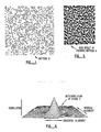
- Figure 1 is an example of one such pattern.
- the image is digitized and filtered to enhance the low frequency information in the pattern while attenuating the high frequency information. Destruction of detailed fine information in this manner makes our invention less sensitive to noise and the optical vagaries of the measurement apparatus. Correlation techniques may then be employed to determine alignment and/or critical dimensions of the integrated circuit.
- the system we have developed is insensitive to many process and sensor-related distortions which appear in images of small features.
- the technique also permits superimposition of two different patterns while enabling measurement of the position of each of them. Thus, if one pattern is defined on the wafer, and the second is placed in photoresist on top of the first, the relative alignment of the two patterns may be automatically determined.
- a method of determining the alignment of regions formed on a semiconductor structure during separate process steps includes the steps of defining a first irregular pattern of elements at a first location on the semiconductor structure during a first process step, defining a second irregular pattern of elements also at the first location on the semiconductor structure during the second process step, acquiring an image of both the first and second patterns at the first location to provide an image thereof, filtering the image to attenuate at least some higher spatial frequencies while preserving at least some lower spatial frequencies to thereby provide a filtered image, and comparing the filtered image with the stored image of at least one of the first or the second pattern to thereby determine the alignment of regions on the semiconductor structure.
- first and second patterns are spaced apart from each other to enable alignment by measurement of the distance between the two patterns.
- obscuring bars are extended through parts of the pattern to hide edges of the individual elements, and enable determination of critical dimensions on the semiconductor structure.
- Our invention includes a method for measuring alignment and measuring critical dimensions on an integrated circuit structure as well as apparatus for carrying out that method. The method is described below, followed by a description of the apparatus.
- Our method employs alignment targets which are built up from isolated fine scale marks, typically marks fabricated at the feature size limit of the process employed to manufacture the integrated circuit. In a preferred embodiment, these fine marks are spread out in a pattern in a two-dimensional array to form a target. Typically, the target will occupy a region of the integrated circuit where circuitry is not to be formed, for example, between bonding pads or in a region interior to the bonding pads.
- our fine scale features consist of small square "dots" distributed in an array.
- the array consists of a matrix of 50 by 50 potential dot locations, with each potential dot being separated from its neighbors by the minimum dimension, i.e., one dot width.
- Figure 1 is an example of such a matrix.
- the actual locations for dots in the array of 50 by 50 potential dots are randomly selected.
- the determination of whether to place a dot in a given location is made employing a random number generator with a 50% probability at each location.
- the pattern (“A) shown in Figure 1 is not repeating and has a large low frequency content of spatial information, that is, the dots and spaces tend to organize themselves into clusters.
- the pattern depicted might be fabricated by etching, oxidizing, diffusion, ion implantation, or any other well known process by which a detectable pattern may be formed in an integrated circuit structure.
- the particular pattern employed is not critical to our invention. Almost any pattern with sufficient low frequency structure may be used, including regular patterns. If regular patterns are chosen, then alignment can be made to a single instance of the pattern, but which instance must be otherwise specified. It is desirable for the pattern to contain low frequency information on two independent axes if alignment in two dimensions is sought. To provide relative insensitivity to optical distortion, high frequency noise and aliasing, the two-dimensional power spectrum of the pattern, should have significant energy distributed over at least an annulus centered on the origin of the power spectrum.
- a second pattern having small sparse elements will be formed in the next layer of the integrated circuit in proximity, but not overlying, the pattern shown in Figure 1.
- the pattern shown in Figure 1 is formed in the semiconductor wafer 10 itself, then another pattern 24 may be formed in photoresist layer 20 spaced apart from the pattern in wafer 10.
- pattern 24 usually will be identical to pattern 12, although this is not necessary.
- alignment of pattern 24 in the photoresist with the pattern 12 in the wafer 10 may be verified using the method of our invention.
- the proper alignment of the two patterns verifies the proper alignment of the two layers and all of the components fabricated therein or thereby.
- the alignment of the components to be formed using the photoresist 20 with the underlying wafer 10 may be verified before the the components are formed in the integrated circuit, that is, before the diffusion etching or other step is carried out.
- the layer of photoresist may be stripped from the wafer (using well known techniques), a new layer of photoresist applied, and a new pattern defined therein. Fabricating the circuit in this manner assures that all of the regions formed in the wafer are properly aligned with respect to each other--eliminating mask misalignment as a source of reduced yield.
- images of the two targets 12 and 24 are acquired using conventional optical or scanning electron microscope technology. Once the image is acquired, it is digitized and a filtering operation is performed to enhance the low frequency structure in the pattern while attenuating the high frequency information. The result is a filtered image such as depicted in Figure 3.
- a Laplacian of Gaussian ( ⁇ 2G) convolution operator is used.
- the Gaussian is a two-dimensional Gaussian which functions to low pass filter the image in a way that attenuates high spatial frequencies while preserving the geometric structure at lower spatial frequencies.
- the size of the Gaussian controls the scale at which structure remains in the filtered image.
- the Laplacian term detects locations in the low pass filtered image where local maxima in the rate of brightness change occur. These locations coincide closely with the locations where the Laplacian has zero value.
- our technique exhibits in its sign pattern structures correlated with the clustering structure of the original dot pattern and not with individual dots. Because the sign pattern is thus tied to the overall position of the dot pattern on the image surface, and not with any particular location for any finer feature, it is insensitive to small distortions such as fringe effects, interference, dirt, noise, etc., which are present in the imaging. Because this technique captures coarse scale structure of the patterns and is relatively insensitive to high frequency noise, it is ideally suited to scanning electron microscope images of the patterns, which typically exhibit significant noise.
- the correlation of C(x,y) when the image I(x,y) is taken to be Gaussian white noise has the form where k is a constant and W is the diameter of the negative central region of the ⁇ 2G convolution function.
- the correlation R s ( ⁇ ) of the sign of Eq. (3), S(x,y) sgn[C(x,y)], obeys an arcsin law when C is a Gaussian random process.
- Figure 4 shows the correlation function of the sign cf a Laplacian of Gaussian convolution.
- Figure 4 when two patterns such as depicted in Figure 3 are compared with each other, a single strongly correlated location, corresponding to the peak of the cone in Figure 4, results. Misalignment, either horizontally or vertically, by any significant amount, results in a much lower correlation.
- the width of the base of the cone is controlled largely by the size of the filter employed, with larger filters providing broader cones. Sharpness of the peak is due to the binary nature of the filtered image.
- the use of the sign, rather than the raw convolution values, also causes the correlation peak to be normalized with a height of one in the absence of noise.
- a model of the surface may be constructed and the peak location estimated with great accuracy.
- the separation between the peaks may be accurately calculated and compared with the desired value to thereby provide an indication of the respective alignment of the two targets.
- each of the targets 12 and 24 was formed at the same time as other regions in that layer of the semiconductor structure, their relative alignment also provides information about the relative alignment of everything in the respective layers.
- a second target on wafer 10 or layer 20 would allow triangulation to measure offset in a perpendicular orientation to Figure 2b.
- the targets are shown as in the wafer and in photoresist on the wafer, such targets could be formed in any two layers if it is desired to determine their relative alignment, for example, in a silicon nitride masking layer and in a second layer of metal connections.
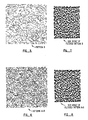
- Figure 5 illustrates another irregular dot pattern ("B") fabricated at a desired location on a semiconductor structure.
- the individual "dots” are spaced apart by one dot height and width.
- this second independent pattern “B” By superimposing this second independent pattern “B” on the first pattern “A” with the dots of pattern “B” falling into the spaces of pattern “A,” each pattern may be treated as noise to the other when the position of each is determined. The positions of the two patterns then may be compared to determine whether the patterns are correctly aligned.
- the pattern "A+B" shown in Figure 6 is an example of this approach. It has been created by combining the pattern depicted in Figure 1 with that shown in Figure 5.
- Each of Figures 1 and 5 have dot patterns which are spaced on a distance which is twice the dot diameter.
- one of the patterns is shifted by one dot diameter to the left and down before being combined with the other pattern. In this manner, the dots of the two patterns do not overlap.
- the pattern of Figure 1 will have been formed on the wafer substrate, while the pattern of Figure 5, shifted by one dot diameter both horizontally and vertically, is formed in the overlying photoresist. When viewing the structure from above, both patterns will be visible.
- Figure 7 illustrates the convolution sign pattern achieved using the Laplacian of Gaussian filter described above for the dot pattern of Figure 5.
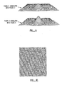
- Figure 8 is a corresponding pattern for Figure 6. Note that the sign pattern of Figure 8 does not resemble either of the patterns of Figure 3 or 7. There is, however, a significant correlation between the sign structure in Figures 8 and 3 and also between Figures 8 and 7. This is illustrated by the correlation plots of Figure 9.
- the upper plot in Figure 9 represents the correlation between Figure 8 and Figure 7, while the lower plot represents the correlation between Figure 8 and Figure 3.
- the position of the peak in the individual plots may be determined by making use of as many measurements of the correlation surface as desired. In this manner the peak of each may be accurately determined.
- the difference in peak positions for the two surfaces represents the alignment error between the two layers. As with the example of Figure 2, this difference may be determined within a very small fraction of the diameter of a pixel. Because the two patterns, A and B, lie in the same part of the camera image and the correlation peaks for each of them are typically separated by less than a dot diameter, the geometric distortion of the optical system has a negligible effect on accuracy.
- the approach described above also can be employed to align masks prior to exposing the photoresist by imaging the mask pattern onto the substrate at suitably low energies (or appropriate wavelengths) to prevent exposure of the photoresist.
- the alignment of the projected pattern and pattern present in the previous layers may be compared.
- any errors detected may be corrected by the stepper or other mask fabrication apparatus.
- Figure 10 illustrates a test pattern for measuring critical dimensions on an individual layer of an integrated circuit structure.
- the pattern of Figure 10 is fabricated by forming on a single layer of the integrated circuit device a pattern of the type depicted in Figure 6, that is, a pattern which is itself a combination of two other constituent patterns.
- the constituent patterns are designed such that obscuring bars which extend through the pattern obscure the right-hand edges of the pattern elements on the "right” pattern and the left-hand edges of the pattern elements on the "left” pattern.
- the pattern formed on the integrated circuit itself consists of two patterns, the pattern is formed in one operation or process step, not two.
- the two constituent patterns are separately stored in the memory of our system and separately filtered.
- the pattern on the integrated circuit then may be employed to measure critical dimensions in the manner described below.
- Figure 11a The manner by which the critical dimensions may be measured is depicted in Figures 11a and 11b.
- Figure 11a the "actual" pattern is underexposed (assuming positive photoresist) in comparison to the nominal "intended" pattern.
- Figure 11b illustrates that when the bars, which the ⁇ 2G filter does not see, are removed, the centers of the individual elements having left edges obscured appear to shift to the right, while the pattern with right edges obscured appears to shift to the left.
- the pattern is overexposed (again, assuming positive photoresist)
- the actual pattern will be smaller than the intended pattern. In this case, the detected position of the pattern with left edges obscured appears to shift to the left, while the pattern with right edges obscured appears to shift to the right.
- the image of the complete pattern (both left and right patterns--see, e.g., Figure 10) is acquired and filtered.
- the convolution of the stored "left” pattern is correlated with the combined pattern
- the convolution of the stored "right” pattern is correlated with the combined pattern.
- the correlation peak for the "right” pattern will be shifted away from the "left" pattern's peak. If the fabricated pattern is overexposed, then the correlation peak of the right pattern will appear shifted to the other direction with respect to the left pattern. The displacement between the two peaks thus will indicate the critical dimension error.
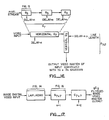
- Figure 12 is a simplified flowchart illustrativelying a preferred embodiment of one method of our invention. The method will be discussed in conjunction with the embodiment of Figures 6 and 9.
- a first irregular pattern A is placed on one layer of the integrated circuit, and a second irregular pattern B (or A in some embodiments) placed on another layer, either immediately above pattern A (or adjacent pattern A).
- An image of the composite pattern is then acquired and correlated with a stored model of pattern A, then with a stored model of pattern B. The difference between the peak positions of these two correlation surfaces represents the alignment error between the two layers.
- Figure 12 is a flowchart illustrating the overall correlation process.
- two inputs are supplied to the process, a stored pattern 30, and a digitized image 31 preferably acquired using an optical or scanning electron microscope.
- An optical microscope is preferred for embodiments where cost is a significant factor in application of the system.
- Adjustments in the size of the image may be made using the magnification control. These adjustments will affect the height of the peak and permit compensating for errors in the SEM preset.
- the stored pattern 30 will consist of digital data representative of the pattern A formed on the underlying semiconductor layer.
- the image 31 will be of the combined patterns A + B.
- any necessary scaling 32 is applied to the pattern to convert it to the proper size for comparison with the acquired image 31.
- scaling is accomplished by using conventional image scaling software. Typically this scaling operation will be done infrequently since the scaled image can be stored and reused. Fine adjustments to the magnification can be made using feedback from the correlation hardware to determine the magnification that yields the highest correlation peak.
- the representation of the stored pattern is filtered to attenuate higher spatial frequencies while preserving some of the lower spatial frequencies.
- This step is represented by block 34.
- the apparatus for performing the filtering is described below.
- the acquired image is also filtered, as shown by step 33.
- the results of the filtered data are each stored, with the image being stored in storage 35 and the representation of the pattern A stored in storage 36. Note that storage 36 can be established once and then reused so long as the patterns and imaging geometry are not changed.
- the contents of the two random access memories 35 and 36 are dumped to an exclusive OR gate 37.
- the exclusive OR gate, 37 in effect, counts the "hits" to determine the correlation between the stored pattern 30 and the image 31.
- the digital representations of the images may be shifted with respect to each other for comparison.
- Counter 38 will count the hits for each shift, in effect, enabling the microprocessor 39 to measure selected points on the peaked correlation surface. Once a sufficient number of measurements have been made, the location of the peak can be estimated.
- the procedure of Figure 12 may be repeated, this time with the stored pattern representing pattern B and the scanning electron microscope image again representing the combined patterns.
- the correlation surface for pattern B correlated with the combination of patterns A and B may be determined. Once the two peaks are determined, the alignment error is represented by the distance between the two peaks.
- the images acquired or retrieved must be processed much more rapidly than a general purpose digital computer would permit. Accordingly, one of us has developed certain special purpose hardware for performing the filtering functions at a sufficiently high rate to enable alignment measurements to be made in less than 0.1 seconds.
- the pattern to be filtered consists of approximately 50 by 50 elements and is displayed in an area of approximately 500 by 500 pixels.
- the first step of our method is to apply the Laplacian function.
- the Laplacian function first provides certain advantages.
- the video signal is centered on zero and then smoothed. This allows better use of n bit integer resolution because the n bit numbers are not required to characterize as wide a range of signal as would exist were the Gaussian function applied first.
- Applying the Laplacian first reduces the amountof scaling required through the Gaussian pipeline operation to keep the values in range.
- the 500-pixel square image 40 is shown at the top of Figure 13. If the Laplacian function is to be applied to pixel C, then the 8 bit binary value for each of pixels A-E must be retrieved and appropriately weighted.
- the apparatus of Figure 13 illustrates one technique for retrieving the desired pixels. As the desired pattern is acquired as a noninterlaced video raster scan, either from memory 44 or from microscope 42 and A-D converter 43, at some given instant pixel A will be supplied on line 45. At that point in time, line 46 will carry B, the value received 499 pixels earlier. Similarly, lines 47, 48, and 49 will hold pixels C, D, and E, respectively, which were received 500, 501 and 1000 pixels earlier than A.
- this configuration produces 5 simultaneous samples making a cross pattern off of the image as shown at the top of Figure 13.
- the delay elements 50 shown in Figure 13 may comprise any known delay element, for example, a shift register or a random access memory. Switches 51 and 52 control whether the pixels latched are from the retrieved pattern 44 or the acquired image 40.
- Figure 14 illustrates apparatus for obtaining the Laplacian of the acquired pixel values.
- a satisfactory approximation to the Laplacian function at a given pixel location is to apply a weight of 4 to that particular pixel and a weight of -1 to the pixels above, below, to the left, and to the right of the specified pixel.
- the pixel values for pixels A and B are supplied to adder 60, while those for pixels D and E are supplied to adder 61.
- adder 6D supplies an output signal A + B on line 62
- adder 61 supplies an output signal D + E on line 63.
- Another adder 64 connected to receive the signals on line 62 and 63 then supplies an output signal on line 65 indicative of the sum of all of pixels A, B, D, and E.
- the pixel value for pixel C is supplied to a shifter 66. By shifting the pixel value two places left, the value is effectively multiplied by four, and the results supplied on line 67 to subtractor 68.
- Subtractor 68 combines the sum supplied on line 65 with the quadruply-weighted value on line 67 to achieve a new value which approximates the Laplacian at pixel C of the input image.
- the output 68 carries a video raster signal of the Laplacian of the input image. This signal is fed to the next stage of processing, the Gaussian convolver.
- the one-dimensional Gaussian operator may be approximated by a binomial distribution in one dimension.
- the seven point binomial distribution 1, 6, 15, 20, 15, 6, 1 is quite close to the Gaussian.
- Figure 15 illustrates the operation of the three point mechanism, G3.
- a and C are applied to adder 70 and the sum supplied on line 71 to a shifter 72. Shifter 72 shifts the sum of A + C one place to the right, in effect dividing it by two.
- the output signal on line 73 is supplied to adder 74 in conjunction with the binary value for pixel B.
- Adder 74 thereby provides on line 75 a value equal to the sum of the value of pixel B plus one-half the sum of values of pixels A and C. To maintain correct amplitude, this result is shifted right one place by shifter 76, and the result supplied on line 77.
- the result on line 77 is the input signal smoothed by a 3 point binomial distribution. To obtain a finer approximation to the Gaussian, the procedure of Figure 15 may be repeated more than once as shown in Figure 16.
- Figure 16 illustrates how a pipeline of 3 three point Gaussian convolution elements G3 of Figure 15 is configured.
- This device convolves the input video stream with a 7 point binomial approximation to a one-dimensional Gaussian G7. If the delay elements are set to produce a delay of one pixel, this will be a horizontal Gaussian convolution. If the delay elements are set to the line length of the image this will be a vertical convolution.
- FIG. 16 illustrates using a pipeline of two G7 elements to produce a G 7 ⁇ 7 element.
- a larger Gaussian filter than the 7 by 7 operator described is required. Similar techniques as described above could be used to build arbitrarily large filters, however we have found a more efficient approach.
- the input signal has been low pass filtered sufficiently that a subsequent operator that samples only every other pixel will not suffer from aliasing problems.
- a 14 by 14 Gaussian convolution can be approximated by the G 7 ⁇ 7 operator with its points spread out by increasing its horizontal delays from 1 to 2 pixels and its vertical delays from one line length to two line lengths.
- Figure 17 shows two G 7 ⁇ 7 elements used in this way to produce effectively a 21 by 21 Gaussian convolution operator in a video pipeline with the Laplacian operator at the start.
- the result is a ⁇ 2G filtered image which may be supplied to suitable storage means, for example, a random access memory such as described in conjunction with blocks 35 and 36 of Figure 12. Because only the sign of the result is saved, the filtered image will be a binary one, having the appearance, for example, of Figures 3, 7 or 8.
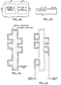
- Figure 18 is a more detailed block diagram of one embodiment of the correlator previously shown in only block form in Figure 12.
- the components shown in Figure 18 are driven by a 10 megaHertz pixel clock.
- the filtered image input data (from Figure 17) is supplied in parallel to six buffer networks 80a-80f shown in Figure 18.
- the contents of one of the buffers 80a is shown in greater detail; similar components make up each of the remaining buffers 80b-80f.
- Buffer 80 includes a 64k-by-1 bit memory 81 for storing approximately one-quarter of the image. Memory 81 corresponds to either block designated storage in Figure 12.
- memory 81 is a static random access memory and stores 256-by-256 pixels of data.
- the choice of the size of memory 81 is arbitrary, and larger or smaller memories may be employed depending upon the particular application for the correlator of Figure 18. Storage of the convolver output data in memory 81 allows scanning of the contents of the memory for purposes of image correlation.
- Address generator counters 82 supply addressing information to the memory 81 to control the location where data from the convolver is stored.
- the address generator counters typically include a first counter for identifying a unique horizontal line, and a second counter for identifying a pixel position on that line.
- the addresses from which data in the static random access memory 81 are read are controlled ultimately by counter 83 and x,y register 84.
- X,y register 84 provides information regarding the center point of a correlation window on the image. By varying the position of the window's center point, one image may be shifted with respect to the other.
- Counter 83 counts the number of points in a window to be compared with the other image data in other buffers, while offset table 85 provides information regarding the offset within the window of each image point to be compared.
- the offset table 85 will typically contain about 4,000 points. Data from the offset table 85 and from the x,y register 84 are combined by adder 86 to provide read address information for memory 81.
- the data from the convolver are supplied both to the left buffer 80a and the right buffers 80b-80f.
- the left buffer, 80a will be filled with convolver data from either the stored pattern or from the SEM.
- the right buffers would then be filled with convolver data from the other source.
- the use of six buffers allows five values to be generated by the exclusive OR networks 90a-90e during each cycle.
- the left buffer allows one value to be used for comparison, while the five right buffers allow five locations in the right image to be examined in parallel. These five ports onto the right image allow 5 points on the same correlation surface, Figure 4, to be computed in parallel. They can also be used to compute a single large correlation window by breaking it into five subwindows.
- the offsets are provided through a look-up table and index to each point in the correlation window. This allows comparison of any desired set of points in one image with any desired set of points in another image. This facility allows correcting for fixed geometric distortions between the two images. It also allows placing more emphasis on the center of the correlation window by spacing the samples more closely near the center of the image.
- Each of the exclusive OR networks 90a-90e contains a latch 91, an exclusive OR gate 92, and one or more counters depending upon the number of bits of counting desired.
- Latch 91 holds the output value from the left buffer and one of the right buffers (depending upon which exclusive OR network) and supplies the resulting data to the exclusive OR gate 92.
- XOR gate 92 drives desired counters to provide as many bits of accuracy as desired.
- a 12-bit counter 93 is provided by three smaller 4-bit counters. Read enable lines coupled to the counters 93 enable supplying the output from a desired counter to a transceiver (not shown).
- patterns already present in the integrated circuit masks and layers are employed in place of the irregular patterns especially generated.
- the patterns in the masks have sufficient low spatial frequency energy.
- the patterns on various layers are somewhat independent from each other and combine in an additive manner.
- a larger area of the "chip" may be employed for measuring the correlation function against a CAD data base for each layer. The larger area available for correlation compensates for the less-than-ideal patterns.
Landscapes
- Physics & Mathematics (AREA)
- General Physics & Mathematics (AREA)
- Engineering & Computer Science (AREA)
- Computer Vision & Pattern Recognition (AREA)
- Theoretical Computer Science (AREA)
- Length Measuring Devices By Optical Means (AREA)
- Image Analysis (AREA)
- Exposure And Positioning Against Photoresist Photosensitive Materials (AREA)
- Container, Conveyance, Adherence, Positioning, Of Wafer (AREA)
- Exposure Of Semiconductors, Excluding Electron Or Ion Beam Exposure (AREA)
- Testing Or Measuring Of Semiconductors Or The Like (AREA)
Applications Claiming Priority (2)
| Application Number | Priority Date | Filing Date | Title |
|---|---|---|---|
| US88905586A | 1986-07-22 | 1986-07-22 | |
| US889055 | 1986-07-22 |
Publications (2)
| Publication Number | Publication Date |
|---|---|
| EP0254644A2 true EP0254644A2 (de) | 1988-01-27 |
| EP0254644A3 EP0254644A3 (de) | 1990-07-18 |
Family
ID=25394438
Family Applications (1)
| Application Number | Title | Priority Date | Filing Date |
|---|---|---|---|
| EP87401705A Withdrawn EP0254644A3 (de) | 1986-07-22 | 1987-07-22 | Maskenausrichtung und Messung von kritischen Dimensionen in integrierten Schaltungen |
Country Status (2)
| Country | Link |
|---|---|
| EP (1) | EP0254644A3 (de) |
| JP (1) | JPS63170936A (de) |
Cited By (16)
| Publication number | Priority date | Publication date | Assignee | Title |
|---|---|---|---|---|
| EP0381067A3 (de) * | 1989-01-31 | 1992-08-12 | Schlumberger Technologies, Inc. | Verfahren zur C.A.D.-Modellspeicherung auf Videobildern mit Addierung der Unordnung |
| EP0373614A3 (de) * | 1988-12-16 | 1992-08-12 | Schlumberger Technologies Inc | Verfahren zur direkten Volumenmessung von dreidimensionalen Objekten in Stereobildern |
| EP0923050A3 (de) * | 1997-12-11 | 2002-07-31 | Affymetrix, Inc. (a California Corporation) | Systeme und Verfahren zur Ausrichtung eines abgetasteten Bildes |
| GB2383411A (en) * | 2001-08-06 | 2003-06-25 | Mitutoyo Corp | Image correlation system having reduced computational loads |
| EP1107184A3 (de) * | 1999-12-06 | 2003-09-17 | Xerox Corporation | Verfahren und Gerät zur Registrierung, Anzeigung und Dekodierung von räumlich registrierten Informationen |
| EP1061417A3 (de) * | 1999-06-17 | 2004-05-19 | Infineon Technologies AG | Verfahren und Vorrichtung zur Überdeckungsmessung |
| US6880755B2 (en) | 1999-12-06 | 2005-04-19 | Xerox Coporation | Method and apparatus for display of spatially registered information using embedded data |
| US6935562B2 (en) | 1999-12-06 | 2005-08-30 | Xerox Corporation | Operations on images having glyph carpets |
| US6990254B2 (en) | 2001-08-06 | 2006-01-24 | Mitutoyo Corporation | Systems and methods for correlating images in an image correlation system with reduced computational loads |
| US6996291B2 (en) | 2001-08-06 | 2006-02-07 | Mitutoyo Corporation | Systems and methods for correlating images in an image correlation system with reduced computational loads |
| GB2454712A (en) * | 2007-11-16 | 2009-05-20 | Snell & Wilcox Ltd | Image sequence processing methods based on image features with low spatial frequency energy |
| US8055098B2 (en) | 2006-01-27 | 2011-11-08 | Affymetrix, Inc. | System, method, and product for imaging probe arrays with small feature sizes |
| US8526764B2 (en) | 2007-11-16 | 2013-09-03 | Snell Limited | Re-sizing image sequences |
| US9445025B2 (en) | 2006-01-27 | 2016-09-13 | Affymetrix, Inc. | System, method, and product for imaging probe arrays with small feature sizes |
| WO2020031041A1 (en) * | 2018-08-06 | 2020-02-13 | Richard Aras | Multi-axis position sensing system |
| CN114358168A (zh) * | 2021-12-29 | 2022-04-15 | 苏州赛美特科技有限公司 | 一种数据对比方法、装置设备及存储介质 |
Family Cites Families (3)
| Publication number | Priority date | Publication date | Assignee | Title |
|---|---|---|---|---|
| GB2067744B (en) * | 1980-01-09 | 1983-11-16 | Goodyear Aerospace Corp | Digital video correlator |
| US4579455A (en) * | 1983-05-09 | 1986-04-01 | Kla Instruments Corporation | Photomask inspection apparatus and method with improved defect detection |
| JPS60253368A (ja) * | 1983-11-10 | 1985-12-14 | Dainippon Screen Mfg Co Ltd | 複製画像記録表示等に於けるjag除去方法 |
-
1987
- 1987-07-22 JP JP62181267A patent/JPS63170936A/ja active Pending
- 1987-07-22 EP EP87401705A patent/EP0254644A3/de not_active Withdrawn
Cited By (21)
| Publication number | Priority date | Publication date | Assignee | Title |
|---|---|---|---|---|
| EP0373614A3 (de) * | 1988-12-16 | 1992-08-12 | Schlumberger Technologies Inc | Verfahren zur direkten Volumenmessung von dreidimensionalen Objekten in Stereobildern |
| EP0381067A3 (de) * | 1989-01-31 | 1992-08-12 | Schlumberger Technologies, Inc. | Verfahren zur C.A.D.-Modellspeicherung auf Videobildern mit Addierung der Unordnung |
| EP0923050A3 (de) * | 1997-12-11 | 2002-07-31 | Affymetrix, Inc. (a California Corporation) | Systeme und Verfahren zur Ausrichtung eines abgetasteten Bildes |
| US6611767B1 (en) | 1997-12-11 | 2003-08-26 | Affymetrix, Inc. | Scanned image alignment systems and methods |
| EP1061417A3 (de) * | 1999-06-17 | 2004-05-19 | Infineon Technologies AG | Verfahren und Vorrichtung zur Überdeckungsmessung |
| US6935562B2 (en) | 1999-12-06 | 2005-08-30 | Xerox Corporation | Operations on images having glyph carpets |
| EP1107184A3 (de) * | 1999-12-06 | 2003-09-17 | Xerox Corporation | Verfahren und Gerät zur Registrierung, Anzeigung und Dekodierung von räumlich registrierten Informationen |
| US6880755B2 (en) | 1999-12-06 | 2005-04-19 | Xerox Coporation | Method and apparatus for display of spatially registered information using embedded data |
| US6990254B2 (en) | 2001-08-06 | 2006-01-24 | Mitutoyo Corporation | Systems and methods for correlating images in an image correlation system with reduced computational loads |
| GB2383411B (en) * | 2001-08-06 | 2005-11-09 | Mitutoyo Corp | Systems and methods for correlating images in an image correlation system with reduced computational loads |
| GB2383411A (en) * | 2001-08-06 | 2003-06-25 | Mitutoyo Corp | Image correlation system having reduced computational loads |
| US6996291B2 (en) | 2001-08-06 | 2006-02-07 | Mitutoyo Corporation | Systems and methods for correlating images in an image correlation system with reduced computational loads |
| US8055098B2 (en) | 2006-01-27 | 2011-11-08 | Affymetrix, Inc. | System, method, and product for imaging probe arrays with small feature sizes |
| US8520976B2 (en) | 2006-01-27 | 2013-08-27 | Affymetrix, Inc. | System, method, and product for imaging probe arrays with small feature size |
| US9445025B2 (en) | 2006-01-27 | 2016-09-13 | Affymetrix, Inc. | System, method, and product for imaging probe arrays with small feature sizes |
| GB2454712A (en) * | 2007-11-16 | 2009-05-20 | Snell & Wilcox Ltd | Image sequence processing methods based on image features with low spatial frequency energy |
| US8526764B2 (en) | 2007-11-16 | 2013-09-03 | Snell Limited | Re-sizing image sequences |
| WO2020031041A1 (en) * | 2018-08-06 | 2020-02-13 | Richard Aras | Multi-axis position sensing system |
| CN112585645A (zh) * | 2018-08-06 | 2021-03-30 | 理查德·阿拉斯 | 多轴位置感测系统 |
| US11620466B2 (en) | 2018-08-06 | 2023-04-04 | Anemos Technology Limited | Multi-axis position sensing system |
| CN114358168A (zh) * | 2021-12-29 | 2022-04-15 | 苏州赛美特科技有限公司 | 一种数据对比方法、装置设备及存储介质 |
Also Published As
| Publication number | Publication date |
|---|---|
| JPS63170936A (ja) | 1988-07-14 |
| EP0254644A3 (de) | 1990-07-18 |
Similar Documents
| Publication | Publication Date | Title |
|---|---|---|
| US5109430A (en) | Mask alignment and measurement of critical dimensions in integrated circuits | |
| US5119444A (en) | System for expedited computation of laplacian and gaussian filters and correlation of their outputs for image processing | |
| EP0254644A2 (de) | Maskenausrichtung und Messung von kritischen Dimensionen in integrierten Schaltungen | |
| US5604819A (en) | Determining offset between images of an IC | |
| US6865288B1 (en) | Pattern inspection method and apparatus | |
| US4783826A (en) | Pattern inspection system | |
| DE4438278C2 (de) | Verfahren zum Erzeugen einer Toleranzwertdatenbank und System zum Prüfen von Leiterplatten unter Anwendung der Toleranzwertdatenbank | |
| CA1150418A (en) | Automatic mask alignment | |
| JP2000208575A (ja) | 形状特徴に基づく欠陥検出方法及び装置 | |
| Xie et al. | A golden-template self-generating method for patterned wafer inspection | |
| EP0370323A3 (de) | Verfahren und Geräte zum Verdichten von Bildern hoher Auflösung | |
| Dom et al. | The P300: A system for automatic patterned wafer inspection | |
| EP0272853A2 (de) | Verfahren und Einrichtung zum automatischen Lesen von Vernier-Mustern | |
| US7915087B2 (en) | Method of arranging dies in a wafer for easy inkless partial wafer process | |
| US7386167B2 (en) | Segmentation technique of an image | |
| DE19947557B4 (de) | Bildverarbeitungsvorrichtung und Bildverarbeitungsverfahren | |
| JPH04252016A (ja) | パターン描画方法 | |
| US6813376B1 (en) | System and method for detecting defects on a structure-bearing surface using optical inspection | |
| JP2004333355A (ja) | 線幅の計測方法 | |
| JPH03201454A (ja) | 半導体装置の位置合わせ方法 | |
| JPH07120696B2 (ja) | 半導体装置の製造方法 | |
| JPH06224099A (ja) | 半導体装置の製造方法 | |
| US5614420A (en) | Method of preventing mask tone error | |
| JPH11316193A (ja) | 画像の領域分割方法 | |
| KR840008221A (ko) | 자동 정렬 시스템 |
Legal Events
| Date | Code | Title | Description |
|---|---|---|---|
| PUAI | Public reference made under article 153(3) epc to a published international application that has entered the european phase |
Free format text: ORIGINAL CODE: 0009012 |
|
| AK | Designated contracting states |
Kind code of ref document: A2 Designated state(s): BE CH DE FR GB LI LU NL |
|
| PUAL | Search report despatched |
Free format text: ORIGINAL CODE: 0009013 |
|
| AK | Designated contracting states |
Kind code of ref document: A3 Designated state(s): BE CH DE FR GB LI LU NL |
|
| 17P | Request for examination filed |
Effective date: 19901221 |
|
| RAP1 | Party data changed (applicant data changed or rights of an application transferred) |
Owner name: SCHLUMBERGER TECHNOLOGIES, INC. |
|
| 17Q | First examination report despatched |
Effective date: 19920917 |
|
| STAA | Information on the status of an ep patent application or granted ep patent |
Free format text: STATUS: THE APPLICATION IS DEEMED TO BE WITHDRAWN |
|
| 18D | Application deemed to be withdrawn |
Effective date: 19930722 |
|
| RIN1 | Information on inventor provided before grant (corrected) |
Inventor name: NISHIHARA, KEITH H. Inventor name: CROSSLEY, P.A. |