EP0250983B1 - Reflective coating for solid-state scintillator bar - Google Patents
Reflective coating for solid-state scintillator bar Download PDFInfo
- Publication number
- EP0250983B1 EP0250983B1 EP87108495A EP87108495A EP0250983B1 EP 0250983 B1 EP0250983 B1 EP 0250983B1 EP 87108495 A EP87108495 A EP 87108495A EP 87108495 A EP87108495 A EP 87108495A EP 0250983 B1 EP0250983 B1 EP 0250983B1
- Authority
- EP
- European Patent Office
- Prior art keywords
- layer
- bar
- multilayer film
- film according
- scintillator
- Prior art date
- Legal status (The legal status is an assumption and is not a legal conclusion. Google has not performed a legal analysis and makes no representation as to the accuracy of the status listed.)
- Expired - Lifetime
Links
Images


Classifications
-
- G—PHYSICS
- G06—COMPUTING OR CALCULATING; COUNTING
- G06T—IMAGE DATA PROCESSING OR GENERATION, IN GENERAL
- G06T1/00—General purpose image data processing
-
- G—PHYSICS
- G01—MEASURING; TESTING
- G01T—MEASUREMENT OF NUCLEAR OR X-RADIATION
- G01T1/00—Measuring X-radiation, gamma radiation, corpuscular radiation, or cosmic radiation
- G01T1/16—Measuring radiation intensity
- G01T1/20—Measuring radiation intensity with scintillation detectors
- G01T1/2002—Optical details, e.g. reflecting or diffusing layers
-
- G—PHYSICS
- G01—MEASURING; TESTING
- G01T—MEASUREMENT OF NUCLEAR OR X-RADIATION
- G01T1/00—Measuring X-radiation, gamma radiation, corpuscular radiation, or cosmic radiation
- G01T1/16—Measuring radiation intensity
- G01T1/20—Measuring radiation intensity with scintillation detectors
-
- Y—GENERAL TAGGING OF NEW TECHNOLOGICAL DEVELOPMENTS; GENERAL TAGGING OF CROSS-SECTIONAL TECHNOLOGIES SPANNING OVER SEVERAL SECTIONS OF THE IPC; TECHNICAL SUBJECTS COVERED BY FORMER USPC CROSS-REFERENCE ART COLLECTIONS [XRACs] AND DIGESTS
- Y10—TECHNICAL SUBJECTS COVERED BY FORMER USPC
- Y10T—TECHNICAL SUBJECTS COVERED BY FORMER US CLASSIFICATION
- Y10T428/00—Stock material or miscellaneous articles
- Y10T428/28—Web or sheet containing structurally defined element or component and having an adhesive outermost layer
- Y10T428/2804—Next to metal
-
- Y—GENERAL TAGGING OF NEW TECHNOLOGICAL DEVELOPMENTS; GENERAL TAGGING OF CROSS-SECTIONAL TECHNOLOGIES SPANNING OVER SEVERAL SECTIONS OF THE IPC; TECHNICAL SUBJECTS COVERED BY FORMER USPC CROSS-REFERENCE ART COLLECTIONS [XRACs] AND DIGESTS
- Y10—TECHNICAL SUBJECTS COVERED BY FORMER USPC
- Y10T—TECHNICAL SUBJECTS COVERED BY FORMER US CLASSIFICATION
- Y10T428/00—Stock material or miscellaneous articles
- Y10T428/28—Web or sheet containing structurally defined element or component and having an adhesive outermost layer
- Y10T428/2848—Three or more layers
Definitions
- the present invention relates to solid state scintillator bars and, more particularly, to coatings for solid state scintillator bars for improving the light output therefrom.
- CT computer tomography
- a CT device employs a fan beam of penetrating radiation passing through a body to be studied and falling on an array of scintillation detectors.
- Each scintillation detector includes a material capable of emitting light when impinged on by the penetrating radiation and a light detector effective to produce an electrical signal in relation to the light it receives.
- the electrical signals from the array of scintillation detectors are processed in a computer to construct an image of the portion of the body being studied.
- the sensitivity of scintillation detectors is particularly important when the body under study is a part of a living human since increased detector sensitivity permits completion of a given study with reduced radiation exposure.
- the scintillator bars in a detector array are spaced closely together with one face, called the front face, receiving the radiation.
- Light emitted within a scintillator bar is transmitted for detection from the face, called the rear face, opposite the front face. Emission of light may take place anywhere within the irradiated volume and may pass in any direction. There is a consequent high probability that emitted light travels toward a face other than the rear face.
- a scintillator bar is generally transparent.
- One technique for encouraging the emitted light to reach the rear face shown, for example in U.S 4,535,243; 3,857,036 and 1,110,621, includes placing specular reflectors on some faces of the scintillator bar. Thus, light impinging on any of the mirrored faces is reflected back into the bar. Eventually, some of the reflected light reaches the rear face and be detected. Several types of loss occur in this process making the light output less than is desired. First, light striking a specularly reflecting surface at close to normal incidence may require many reflections before it reaches the rear face. A good reflector such as, for example, silver, reflects only about 95 percent of the incident light and absorbs the rest.
- a diffuse reflector such as, for example, a paint layer of titanium dioxide.
- titanium dioxide acts as a scatterer of light rather than a reflector. Light impinging on it at normal incidence, for example, is emitted with a generally cosine distribution. Thus, a much greater proportion of the impinging energy is directed back into the bar at shallow angles effective for reaching the rear face with less interaction with the other faces.
- Diffuse reflectors rely on the scattering of light by particles of high refractive index rather than on reflection. Thus a relativity thick coating is required to return most of the light to the scintillator bar.
- modern scintillator arrays arrange their scintillator bars in tight proximity without separators therebetween. Optical crosstalk between the scintillator bars is suppressed by making the surface coating substantially opaque. This also requires a relatively thick paint coating on the order of about 0.0355 mm, (0.0014 inch). The opacity may be improved with a coating of an opaque material such as a metal.
- Thickness uniformity of the paint coating is critical to performance of the array. To obtain it, the paint coating is hand finished using an abrasive, before applying the opaque coating. Such hand finishing is the consuming and risks damaging the product, thereby increasing the scrap rate.
- the present invention provides a multilayer film for coating an exterior of a scintillation bar characterized in that it comprises:
- the light-diffusing material and the specularly reflecting layer cooperate to retain light within the bar, direct light in random directions within the bar, and block optical crosstalk between adjacent bars.
- a preform consisting of a single piece of film may be used for covering five sides of the bar.
- a scintillation bar for a scintillation detector comprising: a substantially parallelipiped bar of a solid state scintillation material, a reflective coating on at least one surface of the bar, the reflective coating consisting of the said multilayer film, the adherent layer of said film being adhered to the at least one surface.
- a preform for a reflective coating on a scintillation bar comprised of said multilayer film said preform having a shape for fitting at least two contiguous surfaces of the scintillation bar.
- a method for providing a reflective coating on a scintillation bar comprising: mixing a predetermined amount of a diffusely reflecting material in a clear pressure sensitive adhesive, spreading the pressure sensitive material on a clear plastic layer, forming a specularly reflecting layer between the clear plastic layer and a protective layer, and adhering a surface of the pressure sensitive adhesive to a surface of the scintillation bar.
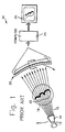
- FIG. 1 there is shown, generally at 10, a CT imaging system to which the present invention may be applied.
- An X-ray source 12, together with a collimator 14 produces a fan-shaped beam 16 which passes through a patient aperture 18 on its way to a scintillation detector array 20.
- a patient 22 in patient aperture 18 selectively absorbs the X radiation passing therethrough, whereby the outputs of individual scintillation detectors in scintillation detector array 20 arm varied.
- At least one of X-ray source 12 and scintillation detector array 20 are rotated about patient 22 for producing a large number of data points.
- the output of all detectors in scintillation detector array 20 are applied to a computer 21 wherein the plurality of data points are analyzed by well-known methods for synthesizing an image for display on a display device 25 such as, for example, a cathode ray tube.
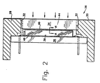
- FIG. 2 a single scintillation detector cell 26 of scintillation detector array 20 is shown.
- Supports 28 and 30 contain a plurality of slots 32 each opposed pair of which receive the ends of a collimator bar 34 of a dense material such as, for example, tungsten.
- a support plate 36 includes a detector diode 38, attached to a front face thereof and, forward of detector diode 38, and in registry therewith, a scintillator bar 40.
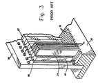
- Fig. 3 from which support 28 is omitted for clarity, adjacent scintillator bars 40, and their associated detector diodes 38, are stacked close together on support plate 36 to form a detector module 42.
- Each collimator bar 34 is aligned with the interface between an adjacent pair of scintillator bars 40.
- Each adjacent pair of collimator bars 34 defines a detector channel 44.
- X radiation passes through a detector channel 44 to impinge upon a front face 16 of scintillator bar 40.
- Light is emitted within scintillator bar 40 for transmission through a rear face 48 to detector diode 38.
- a substantial distance is required between front face 46 and rear face 48, both to provide sufficient interaction with the X radiation, and to absorb a sufficient fraction of the radiation to protect detector diode 38.
- light emitted near front face 46 must find its way a substantial distance through scintillator bar 40 before detection.
- a top view of scintillator bar 40 illustrates a light path where side walls 52 are coated with a specular reflector.
- a quantum of light emitted from a location 50 and directed at near normal incidence to one side wall 52 is specularly reflected toward the opposed side wall 52 to impinge thereon at substantially the same incidence angle. So many reflections result that losses at each reflection, and absorption along each path, absorb substantially all of the light before it reaches rear face 48 for transmission to detector diode 38.
- Fig. 5 shows a similar geometry except that, instead of a specular reflector on side walls 52, a diffuse reflector is provided. Light from location 50 impinging on side wall 52 is re-emitted in essentially random directions. As a consequence, a higher probability of diffusely reflected light reaching rear face 48 is obtained.
- a diffusely reflecting layer of paint is applied to five sides of scintillator bar 40.
- the paint layer is thick enough, and contains sufficient diffracting particles, to achieve a light attenuation of about 98 percent at its outer surface contiguous to the next scintillator bar 40 in detector module 42. It is customary to include an outer opaque coating of paint or metal to block eternal transmission of light to the next scintillator bar 40 for reducing optical crosstalk.
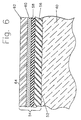
- a multilayer reflecting film 54 is disposed on a surface such as, for example, side wall 52 of scintillator bar 40.
- Multilayer reflecting film 54 includes an adherent layer 56 containing a small percentage by weight of diffusing particles such as, for example, titanium dioxide.
- a clear layer 58 of a plastic having a suitably low index of refraction is disposed upon adherent layer 56.
- a specularly reflecting layer 60 atop clear layer 58 reflects any light having passed through adherent layer 56 and clear layer 58 back toward side wall 52.
- a protective layer 62 lies atop specularly reflecting layer 60.
- Adherent layer 56 is any suitable clear pressure-sensitive adhesive having mixed therein diffusing particles.
- adherent layer 56 is a clear acrylic pressure sensitive adhesive having from 10 to 30 percent by weight of titanium dioxide uniformly dispersed therein. This amount of titanium dioxide is insufficient to attenuate fully the light in its passage therethrough. Thus, reflection by specularly reflecting layer 60 is relied on to return the light passing through adherent layer 56 toward side wall 52.
- the maximum amount of titanium dioxide in adherent layer 56 is limited by its effect on the properties of the adhesive in adherent layer 56. As more titanium dioxide is added to the arterial of adherent layer 56, the mixture becomes more viscous and more difficult to spread in a uniform thin layer. In addition, its tackiness, or ability to adhere to side wall 52, decreases. We have found that a weight percent of from 10 percent to 30 percent, and most preferably, about 20 percent, in adherent layer 56 is a preferred value giving sufficient light diffusion and retaining satisfactory mechanical properties. The thickness of adherent layer 56 is preferaly within about 10 percent of about 0.0127 mm (0.0005 inch). The thickness of adherent layer 56 and its percentage of titanium dioxide can be traded off to achieve comparable results.
- Clear layer 58 is a clear plastic material, and moot preferably a clear acrylic material having an index of refraction at least as low as the plastic material serving as a binder in adherent layer 56. Clear layer 58 is preferably within about 10 percent of about 0.00254 mm (0.0001 inch) thick. The low refraction index of clear layer 58 enhances the action of specularly reflecting layer 60.
- any convenient technique may be employed for applying adherent layer 56 and clear layer 58.
- any of the following may be suitable: roll coating, doctor blading, silk screening, flame spraying, liquid spraying, sintering, vapor deposition, spin coating and powder coating.
- the coating process selected must be one which is capable of producing a layer having the required uniformity.
- Specularly reflecting layer 60 is preferably metallic and most preferably silver. Gold or aluminium may be used with the possibility of a reduction in light output.
- Protective layer 62 is preferably of a polyester having a thickness of within about 10 percent of about (0.0005 inch) 0.0127 mm.
- the total thickness of reflecting film 54 is about 0.0279 mm (0.0011 inch) with adherence of about 10 percent. This is a thinner layer and offers improved uniformity and repeatability than is attainable with prior methods. In addition, substantially complete absence of optical crosstalk between adjacent scintillator bars 40 is achieved.
- specularly reflecting layer 60 is coated on the surface of clear layer 58.
- Such a product io commercially available and provides satisfactory operation.
- specularly reflecting layer 60 being disposed on the outside of the bend, may crack in the vicinity of the corners and thus offer reduced reflectivity.
- specularly reflocting layer 60 is coated on the inner surface of protective layer 62 by conventional methods such as, for example, by sputtering, before affixing clear layer 58 and adhesive layer 56 thereto. With this structure, specularly reflecting layer 60 is on the inside of the band at corners and avoids cracking.
- side wall 52 may be polished to improve light output.
- release layer 66 may be, for example, a paper treated with a silicone material to limit its adhesion to adherent layer 56.
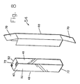
- multilayer reflecting film 54 may be cut into a preform 68 to fit the five sides of scintillator bar 40 to which it is applied. Notches arm removed at each end to leave a tab 70 at each end.
- the main portion of preform 68 is wrapped about front face 46 and side walls 52 and tabs 70 are bent into adhering contact with ends 72 of scintillator bar 40.
- tabs 70 may be omitted and ends 72 may be treated separately using, for example, a separate piece of reflecting film 54. Ends 72 may be treated using prior-art methods of a paint layer since thickness and uniformity have less effect in these locations and optical croostalk between ends 72 of adjacent scintillator bars 40 is not a problem.
- adherent layer 56 should not be taken to preclude materials other than a pressuro-sensitive adhesive in such layer.
- adherent layer 56 may include a curable material capable of being cured by any conventional means into adherence to scintillator bar 40.
- an intermediate layer (not shown) may be employed to provide the required adherence.
- Theme alternatives should employ materials having suitable optical properties according to the foregoing disclosure.
Landscapes
- Physics & Mathematics (AREA)
- General Physics & Mathematics (AREA)
- Health & Medical Sciences (AREA)
- Life Sciences & Earth Sciences (AREA)
- High Energy & Nuclear Physics (AREA)
- Molecular Biology (AREA)
- Spectroscopy & Molecular Physics (AREA)
- Engineering & Computer Science (AREA)
- Theoretical Computer Science (AREA)
- Measurement Of Radiation (AREA)
- Optical Elements Other Than Lenses (AREA)
Applications Claiming Priority (2)
| Application Number | Priority Date | Filing Date | Title |
|---|---|---|---|
| US880190 | 1986-06-30 | ||
| US06/880,190 US4720426A (en) | 1986-06-30 | 1986-06-30 | Reflective coating for solid-state scintillator bar |
Publications (2)
| Publication Number | Publication Date |
|---|---|
| EP0250983A1 EP0250983A1 (en) | 1988-01-07 |
| EP0250983B1 true EP0250983B1 (en) | 1991-04-10 |
Family
ID=25375687
Family Applications (1)
| Application Number | Title | Priority Date | Filing Date |
|---|---|---|---|
| EP87108495A Expired - Lifetime EP0250983B1 (en) | 1986-06-30 | 1987-06-12 | Reflective coating for solid-state scintillator bar |
Country Status (8)
| Country | Link |
|---|---|
| US (1) | US4720426A (enExample) |
| EP (1) | EP0250983B1 (enExample) |
| JP (1) | JPS6325579A (enExample) |
| KR (1) | KR920001244B1 (enExample) |
| CN (1) | CN1008134B (enExample) |
| BR (1) | BR8702553A (enExample) |
| DE (1) | DE3769210D1 (enExample) |
| IL (1) | IL82464A (enExample) |
Families Citing this family (135)
| Publication number | Priority date | Publication date | Assignee | Title |
|---|---|---|---|---|
| DE58904033D1 (de) * | 1988-02-19 | 1993-05-19 | Siemens Ag | Isoliereinrichtung zum optischen isolieren integrierter komponenten. |
| US5486949A (en) | 1989-06-20 | 1996-01-23 | The Dow Chemical Company | Birefringent interference polarizer |
| JP2621503B2 (ja) * | 1989-09-18 | 1997-06-18 | 富士電機株式会社 | シンチレーション検出器 |
| US5140128A (en) * | 1990-05-03 | 1992-08-18 | General Electric Company | Method and system for providing elements of composite objects |
| US5179284A (en) * | 1991-08-21 | 1993-01-12 | General Electric Company | Solid state radiation imager having a reflective and protective coating |
| US5132539A (en) * | 1991-08-29 | 1992-07-21 | General Electric Company | Planar X-ray imager having a moisture-resistant sealing structure |
| US5208460A (en) * | 1991-09-23 | 1993-05-04 | General Electric Company | Photodetector scintillator radiation imager having high efficiency light collection |
| JP2930823B2 (ja) * | 1991-12-11 | 1999-08-09 | 株式会社東芝 | X線ctスキャナ用検出器及びx線検出装置用シンチレータチャネルセパレータ |
| US5410791A (en) * | 1993-07-01 | 1995-05-02 | General Electric Company | Fabrication chuck |
| US5882774A (en) | 1993-12-21 | 1999-03-16 | Minnesota Mining And Manufacturing Company | Optical film |
| US6025897A (en) | 1993-12-21 | 2000-02-15 | 3M Innovative Properties Co. | Display with reflective polarizer and randomizing cavity |
| US6804058B1 (en) | 1993-12-21 | 2004-10-12 | 3M Innovative Properties Company | Electroluminescent light source and display incorporating same |
| EP0962806B1 (en) * | 1993-12-21 | 2008-12-03 | Minnesota Mining And Manufacturing Company | Multilayered optical film |
| US20070091230A1 (en) * | 1993-12-21 | 2007-04-26 | 3M Innovative Properties Company | Display incorporating reflective polarizer |
| US6498683B2 (en) | 1999-11-22 | 2002-12-24 | 3M Innovative Properties Company | Multilayer optical bodies |
| US6096375A (en) * | 1993-12-21 | 2000-08-01 | 3M Innovative Properties Company | Optical polarizer |
| US5521385A (en) * | 1994-03-01 | 1996-05-28 | Optoscint, Inc. | Long life gamma camera plate assembly with improved reflector system |
| US6101032A (en) | 1994-04-06 | 2000-08-08 | 3M Innovative Properties Company | Light fixture having a multilayer polymeric film |
| US5430298A (en) * | 1994-06-21 | 1995-07-04 | General Electric Company | CT array with improved photosensor linearity and reduced crosstalk |
| US5541421A (en) * | 1994-11-21 | 1996-07-30 | Eastman Kodak Company | Light collector having optically coated acrylic substrate |
| US5751388A (en) | 1995-04-07 | 1998-05-12 | Honeywell Inc. | High efficiency polarized display |
| US6737154B2 (en) | 1995-06-26 | 2004-05-18 | 3M Innovative Properties Company | Multilayer polymer film with additional coatings or layers |
| EP0835294B1 (en) | 1995-06-26 | 2003-01-29 | Minnesota Mining And Manufacturing Company | Light diffusing adhesive |
| US5699188A (en) * | 1995-06-26 | 1997-12-16 | Minnesota Mining And Manufacturing Co. | Metal-coated multilayer mirror |
| JP4122057B2 (ja) | 1995-06-26 | 2008-07-23 | スリーエム カンパニー | 追加のコーティングまたは層を備えた多層ポリマーフィルム |
| EP0832392B1 (en) * | 1995-06-26 | 2003-08-13 | Minnesota Mining And Manufacturing Company | Backlight system with multilayer optical film reflector |
| US6088067A (en) * | 1995-06-26 | 2000-07-11 | 3M Innovative Properties Company | Liquid crystal display projection system using multilayer optical film polarizers |
| AU694884B2 (en) | 1995-06-26 | 1998-07-30 | Minnesota Mining And Manufacturing Company | Transparent multilayer device |
| US6080467A (en) * | 1995-06-26 | 2000-06-27 | 3M Innovative Properties Company | High efficiency optical devices |
| AU708412B2 (en) * | 1995-06-26 | 1999-08-05 | Minnesota Mining And Manufacturing Company | Diffusely reflecting multilayer polarizers and mirrors |
| JP3935936B2 (ja) * | 1995-06-26 | 2007-06-27 | スリーエム カンパニー | 反射偏光型半透過反射体を備えた半透過反射型ディスプレイ |
| US5753918A (en) * | 1995-10-19 | 1998-05-19 | Optoscint, Inc. | Superior performance subassembly for scintillation detection and detectors employing the subassembly |
| US5614721A (en) * | 1995-12-13 | 1997-03-25 | Optoscint, Inc. | Modular gamma camera plate assembly with enhanced energy detection and resolution |
| US6590705B1 (en) * | 1996-02-29 | 2003-07-08 | 3M Innovative Properties Company | Optical film with co-continuous phases |
| BR9707795A (pt) | 1996-02-29 | 1999-07-27 | Minnesota Mining & Mfg | Polarizador de controle de direção película de controle de luz e unidade de apresentação visual |
| US5825543A (en) * | 1996-02-29 | 1998-10-20 | Minnesota Mining And Manufacturing Company | Diffusely reflecting polarizing element including a first birefringent phase and a second phase |
| US5867316A (en) * | 1996-02-29 | 1999-02-02 | Minnesota Mining And Manufacturing Company | Multilayer film having a continuous and disperse phase |
| US5808794A (en) * | 1996-07-31 | 1998-09-15 | Weber; Michael F. | Reflective polarizers having extended red band edge for controlled off axis color |
| FR2768522B1 (fr) * | 1997-09-18 | 1999-10-15 | Commissariat Energie Atomique | Detecteur a scintillation, revetement refracteur pour scintillateur et procede de fabrication d'un tel revetement |
| US6627300B1 (en) | 1997-10-12 | 2003-09-30 | 3M Innovative Properties Company | Optical device containing polymeric material domains having different degrees of randomness |
| US7023602B2 (en) * | 1999-05-17 | 2006-04-04 | 3M Innovative Properties Company | Reflective LCD projection system using wide-angle Cartesian polarizing beam splitter and color separation and recombination prisms |
| US6486997B1 (en) | 1997-10-28 | 2002-11-26 | 3M Innovative Properties Company | Reflective LCD projection system using wide-angle Cartesian polarizing beam splitter |
| US6157490A (en) * | 1998-01-13 | 2000-12-05 | 3M Innovative Properties Company | Optical film with sharpened bandedge |
| US6808658B2 (en) * | 1998-01-13 | 2004-10-26 | 3M Innovative Properties Company | Method for making texture multilayer optical films |
| US6157486A (en) * | 1998-01-13 | 2000-12-05 | 3M Innovative Properties Company | Retroreflective dichroic reflector |
| US6045894A (en) * | 1998-01-13 | 2000-04-04 | 3M Innovative Properties Company | Clear to colored security film |
| US6113811A (en) | 1998-01-13 | 2000-09-05 | 3M Innovative Properties Company | Dichroic polarizing film and optical polarizer containing the film |
| US6120026A (en) * | 1998-01-13 | 2000-09-19 | 3M Innovative Properties Co. | Game with privacy material |
| US6179948B1 (en) | 1998-01-13 | 2001-01-30 | 3M Innovative Properties Company | Optical film and process for manufacture thereof |
| US6967778B1 (en) | 1998-01-13 | 2005-11-22 | 3M Innovative Properties Co. | Optical film with sharpened bandedge |
| US6207260B1 (en) | 1998-01-13 | 2001-03-27 | 3M Innovative Properties Company | Multicomponent optical body |
| US6012820A (en) * | 1998-01-13 | 2000-01-11 | 3M Innovative Properties Compnay | Lighted hand-holdable novelty article |
| US6569515B2 (en) | 1998-01-13 | 2003-05-27 | 3M Innovative Properties Company | Multilayered polymer films with recyclable or recycled layers |
| US6926952B1 (en) * | 1998-01-13 | 2005-08-09 | 3M Innovative Properties Company | Anti-reflective polymer constructions and method for producing same |
| WO1999036478A1 (en) | 1998-01-13 | 1999-07-22 | Minnesota Mining And Manufacturing Company | Color shifting film glitter |
| US6024455A (en) * | 1998-01-13 | 2000-02-15 | 3M Innovative Properties Company | Reflective article with concealed retroreflective pattern |
| US6053795A (en) * | 1998-01-13 | 2000-04-25 | 3M Innovative Properties Company | Toy having image mode and changed image mode |
| US6111697A (en) | 1998-01-13 | 2000-08-29 | 3M Innovative Properties Company | Optical device with a dichroic polarizer and a multilayer optical film |
| US6082876A (en) * | 1998-01-13 | 2000-07-04 | 3M Innovative Properties Company | Hand-holdable toy light tube with color changing film |
| US6049419A (en) | 1998-01-13 | 2000-04-11 | 3M Innovative Properties Co | Multilayer infrared reflecting optical body |
| US6788463B2 (en) * | 1998-01-13 | 2004-09-07 | 3M Innovative Properties Company | Post-formable multilayer optical films and methods of forming |
| US5999317A (en) * | 1998-01-13 | 1999-12-07 | 3M Innovative Properties Company | Toy mirror with transmissive image mode |
| US6531230B1 (en) * | 1998-01-13 | 2003-03-11 | 3M Innovative Properties Company | Color shifting film |
| WO1999036262A2 (en) * | 1998-01-13 | 1999-07-22 | Minnesota Mining And Manufacturing Company | Modified copolyesters and improved multilayer reflective films |
| KR100563159B1 (ko) | 1998-04-24 | 2006-03-22 | 미네소타 마이닝 앤드 매뉴팩춰링 캄파니 | 자기 접착 확산판을 갖춘 광학 부품 |
| US7034306B2 (en) * | 1998-06-18 | 2006-04-25 | Hamamatsu Photonics K.K. | Scintillator panel and radiation image sensor |
| US6256146B1 (en) | 1998-07-31 | 2001-07-03 | 3M Innovative Properties | Post-forming continuous/disperse phase optical bodies |
| US6749427B1 (en) * | 1998-07-31 | 2004-06-15 | 3M Innovative Properties Company | Dental articles including post-formable multilayer optical films |
| US6208466B1 (en) | 1998-11-25 | 2001-03-27 | 3M Innovative Properties Company | Multilayer reflector with selective transmission |
| US20010046086A1 (en) * | 1998-12-23 | 2001-11-29 | 3M Innovative Properties Company | Polymeric interference film |
| US6455140B1 (en) | 1999-01-13 | 2002-09-24 | 3M Innovative Properties Company | Visible mirror film glitter |
| US6218670B1 (en) | 1999-01-29 | 2001-04-17 | Universities Research Association, Inc. | Scintillator reflective layer coextrusion |
| US6322236B1 (en) | 1999-02-09 | 2001-11-27 | 3M Innovative Properties Company | Optical film with defect-reducing surface and method for making same |
| US6381068B1 (en) | 1999-03-19 | 2002-04-30 | 3M Innovative Properties Company | Reflective projection screen and projection system |
| EP1862821A1 (en) * | 1999-04-09 | 2007-12-05 | Hamamatsu Photonics K.K. | Scintillator panel and radiation ray image sensor |
| US6515785B1 (en) | 1999-04-22 | 2003-02-04 | 3M Innovative Properties Company | Optical devices using reflecting polarizing materials |
| US6407862B2 (en) | 1999-05-14 | 2002-06-18 | 3M Innovative Properties Company | Electronic projection system with polymeric film optical components |
| US6972813B1 (en) * | 1999-06-09 | 2005-12-06 | 3M Innovative Properties Company | Optical laminated bodies, lighting equipment and area luminescence equipment |
| US6361735B1 (en) | 1999-09-01 | 2002-03-26 | General Electric Company | Composite ceramic article and method of making |
| AU2515200A (en) | 1999-09-20 | 2001-04-24 | 3M Innovative Properties Company | Optical films having at least one particle-containing layer |
| US6654170B1 (en) | 1999-10-12 | 2003-11-25 | 3M Innovative Properties Company | Optical device having continuous and disperse phases |
| US6673275B1 (en) | 1999-10-12 | 2004-01-06 | 3M Innovative Properties Company | Method for making optical devices from homopolymers |
| US6449093B2 (en) | 1999-10-12 | 2002-09-10 | 3M Innovative Properties Company | Optical bodies made with a birefringent polymer |
| US6264336B1 (en) | 1999-10-22 | 2001-07-24 | 3M Innovative Properties Company | Display apparatus with corrosion-resistant light directing film |
| US6590711B1 (en) | 2000-04-03 | 2003-07-08 | 3M Innovative Properties Co. | Light directing construction having corrosion resistant feature |
| US6590707B1 (en) | 2000-03-31 | 2003-07-08 | 3M Innovative Properties Company | Birefringent reflectors using isotropic materials and form birefringence |
| AU2000266214A1 (en) | 2000-04-13 | 2001-10-30 | 3M Innovative Properties Company | Light stable articles |
| JP2004507781A (ja) | 2000-08-21 | 2004-03-11 | スリーエム イノベイティブ プロパティズ カンパニー | 損失強化型反射光フィルタ |
| AU2001284524A1 (en) * | 2000-09-11 | 2002-03-26 | Hamamatsu Photonics K.K. | Scintillator panel, radiation image sensor and methods of producing them |
| US6479824B1 (en) * | 2000-11-08 | 2002-11-12 | Ge Medical Systems Global Technology Company, Llc | Scintillator arrays for CT imaging and other applications |
| US6534158B2 (en) | 2001-02-16 | 2003-03-18 | 3M Innovative Properties Company | Color shifting film with patterned fluorescent and non-fluorescent colorants |
| US6506480B2 (en) | 2001-02-16 | 2003-01-14 | 3M Innovative Properties Company | Color shifting film with a plurality of fluorescent colorants |
| US6573963B2 (en) | 2001-02-22 | 2003-06-03 | 3M Innovativeproperties Company | Cholesteric liquid crystal optical bodies and methods of manufacture |
| US6917399B2 (en) | 2001-02-22 | 2005-07-12 | 3M Innovative Properties Company | Optical bodies containing cholesteric liquid crystal material and methods of manufacture |
| US6876427B2 (en) | 2001-09-21 | 2005-04-05 | 3M Innovative Properties Company | Cholesteric liquid crystal optical bodies and methods of manufacture and use |
| WO2003100460A1 (en) * | 2002-05-29 | 2003-12-04 | Koninklijke Philips Electronics N.V. | X-ray detector with csi: ti conversion layer |
| WO2004037515A1 (en) * | 2002-10-24 | 2004-05-06 | 3M Innovative Properties Company | Methods of making high gain optical devices having a continuous and dispersive phase |
| US20040219338A1 (en) * | 2003-05-01 | 2004-11-04 | Hebrink Timothy J. | Materials, configurations, and methods for reducing warpage in optical films |
| US20050229838A1 (en) * | 2003-07-07 | 2005-10-20 | Lyons Robert J | Aircraft secondary electric load controlling system |
| US7199369B1 (en) * | 2003-07-16 | 2007-04-03 | Met One Instruments, Inc. | Low threshold level radiation detector |
| US7164134B2 (en) * | 2003-08-01 | 2007-01-16 | General Electric Company | High performance CT reflector for a scintillator array and method for making same |
| US6898265B1 (en) | 2003-11-20 | 2005-05-24 | Ge Medical Systems Global Technology Company, Llc | Scintillator arrays for radiation detectors and methods of manufacture |
| US7019905B2 (en) * | 2003-12-30 | 2006-03-28 | 3M Innovative Properties Company | Multilayer reflector with suppression of high order reflections |
| DE102004021494B4 (de) * | 2004-04-30 | 2006-04-06 | Man Roland Druckmaschinen Ag | Vorrichtung zum Auf- und Abziehen einer Hülse |
| JP2008518280A (ja) * | 2004-10-29 | 2008-05-29 | スリーエム イノベイティブ プロパティズ カンパニー | 環状オレフィンコポリマーを組み入れた光学フィルム |
| US20060159888A1 (en) * | 2004-10-29 | 2006-07-20 | Hebrink Timothy J | Optical films incorporating cyclic olefin copolymers |
| US7329465B2 (en) * | 2004-10-29 | 2008-02-12 | 3M Innovative Properties Company | Optical films incorporating cyclic olefin copolymers |
| US20060093809A1 (en) * | 2004-10-29 | 2006-05-04 | Hebrink Timothy J | Optical bodies and methods for making optical bodies |
| DE602006008994D1 (de) * | 2005-01-13 | 2009-10-22 | Aloka Co Ltd | Szintillatorteil und Herstellungsverfahren dafür sowie Strahlungsmessvorrichtung |
| JP4537322B2 (ja) * | 2005-01-13 | 2010-09-01 | アロカ株式会社 | シンチレータ部材の製造方法及び放射線測定装置の製造方法 |
| US8568869B2 (en) * | 2005-04-06 | 2013-10-29 | 3M Innovative Properties Company | Optical bodies including rough strippable boundary layers and asymmetric surface structures |
| US9709700B2 (en) * | 2005-04-06 | 2017-07-18 | 3M Innovative Properties Company | Optical bodies including rough strippable boundary layers |
| US20060227421A1 (en) * | 2005-04-06 | 2006-10-12 | Stover Carl A | Optical bodies including strippable boundary layers |
| US7180779B2 (en) * | 2005-07-11 | 2007-02-20 | Atmel Corporation | Memory architecture with enhanced over-erase tolerant control gate scheme |
| JP4537327B2 (ja) * | 2006-02-07 | 2010-09-01 | アロカ株式会社 | 放射線測定装置の製造方法及びシンチレータ部材製造方法 |
| WO2009024895A2 (en) * | 2007-08-22 | 2009-02-26 | Koninklijke Philips Electronics N.V. | Reflector and light collimator arrangement for improved light collection in scintillation detectors |
| US8106363B2 (en) * | 2008-04-17 | 2012-01-31 | Carestream Health, Inc. | Digital radiography panel with pressure-sensitive adhesive for optical coupling between scintillator screen and detector and method of manufacture |
| US7977646B2 (en) * | 2008-04-17 | 2011-07-12 | Saint-Gobain Ceramics & Plastics, Inc. | Scintillation detector reflector |
| US8248601B2 (en) * | 2008-09-12 | 2012-08-21 | Siemens Medical Solutions Usa, Inc. | Optical mask for detector optimization |
| CN102227649B (zh) * | 2008-12-17 | 2014-09-03 | 圣戈本陶瓷及塑料股份有限公司 | 闪烁阵列方法以及器具 |
| WO2010075384A2 (en) * | 2008-12-23 | 2010-07-01 | Saint-Gobain Ceramics & Plastics, Inc. | Scintillation separator |
| JP2011044717A (ja) * | 2009-08-20 | 2011-03-03 | Icemos Technology Ltd | 直接ウエハ接合貫通孔フォトダイオード |
| JP2013502595A (ja) * | 2009-08-24 | 2013-01-24 | サン−ゴバン セラミックス アンド プラスティクス,インコーポレイティド | シンチレーション検出器アセンブリ |
| CN102033239B (zh) * | 2009-09-28 | 2013-07-10 | 同方威视技术股份有限公司 | 加速器x射线能量测量系统 |
| EP2486424B1 (en) * | 2009-10-06 | 2016-03-16 | Koninklijke Philips N.V. | Radiation conversion elements with reflectors for radiological imaging apparatus |
| US9057790B2 (en) | 2011-09-30 | 2015-06-16 | Saint-Gobain Ceramics & Plastics, Inc. | Scintillation detection device with pressure sensitive adhesive interfaces |
| CN104903745B (zh) | 2013-01-08 | 2018-07-24 | 斯基恩特-X公司 | 包含多层涂层的x射线闪烁体 |
| JP6079284B2 (ja) * | 2013-02-08 | 2017-02-15 | 株式会社島津製作所 | 放射線検出器および放射線検出器の製造方法 |
| JP6200173B2 (ja) * | 2013-03-21 | 2017-09-20 | キヤノン株式会社 | 放射線検出装置及び放射線検出システム |
| US9599724B2 (en) | 2013-05-08 | 2017-03-21 | Koninklijke Philips N.V. | Gamma radiation detection device |
| CN105556341B (zh) * | 2013-09-18 | 2019-12-03 | 皇家飞利浦有限公司 | 用于增加的性能的经激光蚀刻的闪烁晶体 |
| CN104090291A (zh) * | 2014-07-24 | 2014-10-08 | 重庆大学 | 准直器阵列、工业ct设备线性探测器串扰校正装置及方法 |
| JP2018009803A (ja) * | 2016-07-11 | 2018-01-18 | コニカミノルタ株式会社 | シンチレータパネル |
| JP7494040B2 (ja) * | 2019-07-31 | 2024-06-03 | キヤノン株式会社 | シンチレータユニット、及び放射線検出器 |
| WO2021020491A1 (ja) | 2019-07-31 | 2021-02-04 | キヤノン株式会社 | シンチレータユニット、及び放射線検出器 |
Family Cites Families (5)
| Publication number | Priority date | Publication date | Assignee | Title |
|---|---|---|---|---|
| US2956162A (en) * | 1954-05-25 | 1960-10-11 | Texaco Development Corp | Detection and measurement of penetrative radiation |
| US4110621A (en) * | 1977-03-23 | 1978-08-29 | Butler-Newton, Inc. | Tomography X-ray detector |
| US4107534A (en) * | 1977-06-13 | 1978-08-15 | Piltingsrud Harley V | Plutonium-americium detection probe with frontal light-guide-diffuser |
| US4491732A (en) * | 1982-08-25 | 1985-01-01 | General Electric Company | Optical potting of solid-state detector cells |
| US4533489A (en) * | 1983-12-07 | 1985-08-06 | Harshaw/Filtrol Partnership | Formable light reflective compositions |
-
1986
- 1986-06-30 US US06/880,190 patent/US4720426A/en not_active Expired - Lifetime
-
1987
- 1987-05-06 BR BR8702553A patent/BR8702553A/pt unknown
- 1987-05-10 IL IL82464A patent/IL82464A/xx not_active IP Right Cessation
- 1987-06-12 DE DE8787108495T patent/DE3769210D1/de not_active Expired - Lifetime
- 1987-06-12 EP EP87108495A patent/EP0250983B1/en not_active Expired - Lifetime
- 1987-06-29 CN CN87104468A patent/CN1008134B/zh not_active Expired
- 1987-06-29 KR KR1019870006605A patent/KR920001244B1/ko not_active Expired
- 1987-06-30 JP JP62161411A patent/JPS6325579A/ja active Granted
Also Published As
| Publication number | Publication date |
|---|---|
| DE3769210D1 (de) | 1991-05-16 |
| BR8702553A (pt) | 1988-02-23 |
| CN1008134B (zh) | 1990-05-23 |
| IL82464A0 (en) | 1987-11-30 |
| US4720426A (en) | 1988-01-19 |
| KR880000878A (ko) | 1988-03-30 |
| JPH0531950B2 (enExample) | 1993-05-13 |
| KR920001244B1 (ko) | 1992-02-08 |
| EP0250983A1 (en) | 1988-01-07 |
| JPS6325579A (ja) | 1988-02-03 |
| IL82464A (en) | 1990-08-31 |
| CN87104468A (zh) | 1988-02-03 |
Similar Documents
| Publication | Publication Date | Title |
|---|---|---|
| US4720426A (en) | Reflective coating for solid-state scintillator bar | |
| CN101779145B (zh) | 一种辐射探测方法 | |
| US5055978A (en) | Uniform light source | |
| US6407392B1 (en) | Radiation detector | |
| CA1268360A (en) | Reading device for stimulable phosphor panel | |
| US6885004B2 (en) | High resolution tiled microchannel storage phosphor based radiation sensor | |
| JPS6211313B2 (enExample) | ||
| JP2565278B2 (ja) | 放射線検出器 | |
| US5258145A (en) | Method for manufacturing a high resolution structured x-ray detector | |
| RU2643935C2 (ru) | Устройство (варианты) и способ радиологической визуализации | |
| US3068359A (en) | Scintillator component | |
| US4532425A (en) | Gamma camera with light guide having greater index of refraction | |
| US4739168A (en) | X-ray detector and method for manufacturing the same | |
| GB2224353A (en) | Radiation detector | |
| US6534772B1 (en) | High resolution high output microchannel based radiation sensor | |
| US6516044B1 (en) | Scintillation apparatus and method of light collection for use with a radiation emitting medical imaging scanner | |
| US6369391B1 (en) | Light output optimization | |
| US5206514A (en) | Luminescent storage screen having a stimulable phosphor | |
| EP0469112B1 (en) | Transparent radiation image storage panel | |
| US4204125A (en) | High resolution X-ray intensifying screen with antireflecting substrate | |
| US4970394A (en) | Apparatus for reading-out stimulable phosphor, radiographic recording elements | |
| JP2001516888A (ja) | シンチレーション検出器、シンチレータ用屈折コーティング、および該コーティングの製造プロセス | |
| EP1033587A2 (en) | Radiation image storage panel for double-side reading system | |
| JPS5888685A (ja) | 放射線検出器 | |
| EP1221631A1 (en) | High efficient light guiding means |
Legal Events
| Date | Code | Title | Description |
|---|---|---|---|
| PUAI | Public reference made under article 153(3) epc to a published international application that has entered the european phase |
Free format text: ORIGINAL CODE: 0009012 |
|
| AK | Designated contracting states |
Kind code of ref document: A1 Designated state(s): DE FR GB NL |
|
| 17P | Request for examination filed |
Effective date: 19880620 |
|
| 17Q | First examination report despatched |
Effective date: 19890918 |
|
| DX | Miscellaneous (deleted) | ||
| GRAA | (expected) grant |
Free format text: ORIGINAL CODE: 0009210 |
|
| AK | Designated contracting states |
Kind code of ref document: B1 Designated state(s): DE FR GB NL |
|
| ET | Fr: translation filed | ||
| REF | Corresponds to: |
Ref document number: 3769210 Country of ref document: DE Date of ref document: 19910516 |
|
| PLBE | No opposition filed within time limit |
Free format text: ORIGINAL CODE: 0009261 |
|
| STAA | Information on the status of an ep patent application or granted ep patent |
Free format text: STATUS: NO OPPOSITION FILED WITHIN TIME LIMIT |
|
| 26N | No opposition filed | ||
| PGFP | Annual fee paid to national office [announced via postgrant information from national office to epo] |
Ref country code: GB Payment date: 19920421 Year of fee payment: 6 |
|
| PGFP | Annual fee paid to national office [announced via postgrant information from national office to epo] |
Ref country code: FR Payment date: 19920515 Year of fee payment: 6 |
|
| PG25 | Lapsed in a contracting state [announced via postgrant information from national office to epo] |
Ref country code: GB Effective date: 19930612 |
|
| GBPC | Gb: european patent ceased through non-payment of renewal fee |
Effective date: 19930612 |
|
| PG25 | Lapsed in a contracting state [announced via postgrant information from national office to epo] |
Ref country code: FR Effective date: 19940228 |
|
| REG | Reference to a national code |
Ref country code: FR Ref legal event code: ST |
|
| PGFP | Annual fee paid to national office [announced via postgrant information from national office to epo] |
Ref country code: NL Payment date: 19950522 Year of fee payment: 9 |
|
| PG25 | Lapsed in a contracting state [announced via postgrant information from national office to epo] |
Ref country code: NL Effective date: 19970101 |
|
| NLV4 | Nl: lapsed or anulled due to non-payment of the annual fee |
Effective date: 19970101 |
|
| PGFP | Annual fee paid to national office [announced via postgrant information from national office to epo] |
Ref country code: DE Payment date: 20060731 Year of fee payment: 20 |