EP0250976A1 - Dispositif de traitement de données d'images - Google Patents
Dispositif de traitement de données d'images Download PDFInfo
- Publication number
- EP0250976A1 EP0250976A1 EP87108479A EP87108479A EP0250976A1 EP 0250976 A1 EP0250976 A1 EP 0250976A1 EP 87108479 A EP87108479 A EP 87108479A EP 87108479 A EP87108479 A EP 87108479A EP 0250976 A1 EP0250976 A1 EP 0250976A1
- Authority
- EP
- European Patent Office
- Prior art keywords
- address
- memory
- counter
- image
- counters
- Prior art date
- Legal status (The legal status is an assumption and is not a legal conclusion. Google has not performed a legal analysis and makes no representation as to the accuracy of the status listed.)
- Ceased
Links
Images


Classifications
-
- G—PHYSICS
- G06—COMPUTING; CALCULATING OR COUNTING
- G06F—ELECTRIC DIGITAL DATA PROCESSING
- G06F7/00—Methods or arrangements for processing data by operating upon the order or content of the data handled
- G06F7/76—Arrangements for rearranging, permuting or selecting data according to predetermined rules, independently of the content of the data
- G06F7/78—Arrangements for rearranging, permuting or selecting data according to predetermined rules, independently of the content of the data for changing the order of data flow, e.g. matrix transposition or LIFO buffers; Overflow or underflow handling therefor
- G06F7/785—Arrangements for rearranging, permuting or selecting data according to predetermined rules, independently of the content of the data for changing the order of data flow, e.g. matrix transposition or LIFO buffers; Overflow or underflow handling therefor having a sequence of storage locations each being individually accessible for both enqueue and dequeue operations, e.g. using a RAM
-
- G—PHYSICS
- G06—COMPUTING; CALCULATING OR COUNTING
- G06F—ELECTRIC DIGITAL DATA PROCESSING
- G06F16/00—Information retrieval; Database structures therefor; File system structures therefor
- G06F16/50—Information retrieval; Database structures therefor; File system structures therefor of still image data
- G06F16/51—Indexing; Data structures therefor; Storage structures
-
- G—PHYSICS
- G06—COMPUTING; CALCULATING OR COUNTING
- G06T—IMAGE DATA PROCESSING OR GENERATION, IN GENERAL
- G06T1/00—General purpose image data processing
- G06T1/20—Processor architectures; Processor configuration, e.g. pipelining
-
- G—PHYSICS
- G09—EDUCATION; CRYPTOGRAPHY; DISPLAY; ADVERTISING; SEALS
- G09G—ARRANGEMENTS OR CIRCUITS FOR CONTROL OF INDICATING DEVICES USING STATIC MEANS TO PRESENT VARIABLE INFORMATION
- G09G5/00—Control arrangements or circuits for visual indicators common to cathode-ray tube indicators and other visual indicators
- G09G5/36—Control arrangements or circuits for visual indicators common to cathode-ray tube indicators and other visual indicators characterised by the display of a graphic pattern, e.g. using an all-points-addressable [APA] memory
- G09G5/39—Control of the bit-mapped memory
- G09G5/395—Arrangements specially adapted for transferring the contents of the bit-mapped memory to the screen
-
- G—PHYSICS
- G11—INFORMATION STORAGE
- G11C—STATIC STORES
- G11C8/00—Arrangements for selecting an address in a digital store
- G11C8/04—Arrangements for selecting an address in a digital store using a sequential addressing device, e.g. shift register, counter
Definitions
- the invention relates to an arrangement for processing image data according to the preamble of claim 1.
- Such an arrangement is known from the magazines “Elektronik” 1985, number 5, pages 93 and 94 and "Der Elektroniker” 1985, number 1, pages 59 to 67 .
- the known arrangements contain a plurality of processors which process the image data supplied by a camera or read out from an image memory. As long as the image data is read from the memory in the same order as it was written, there are no problems. It is different, however, if the order is to be changed and each address has to be laboriously calculated using software.
- the present invention has for its object to provide an arrangement of the type specified in the preamble of claim 1, with which the data entered in an image memory can be read quickly, even with the pixel frequency, in a changed order.
- this object is achieved with the measures specified in the characterizing parts of claims 1 and 4.
- the solution according to claim 1 it is achieved that when the read image data is displayed on a display device, the displayed image is rotated by ⁇ 90 ° or 180 ° with respect to the original and is additionally mirrored. If the meters are connected in parallel, a diagonal scan takes place.
- the solution according to claim 4 allows the image data to be read out in any order without stressing the process.
- KA designates a television camera to which an analog-to-digital converter ADU is connected, which converts the analog video signals from the camera into digital signals.
- ADU analog-to-digital converter
- DB1 bus line to which two image memories BSP1, BSP2 and a monitor MO are connected.
- Each image memory is connected to a processor PR1, PR2, of which the processor PR2 is used primarily for image evaluation, while the processor PR1 preprocesses the data contained in the image memory BSP1.
- the main memory of the processor is called ASP.
- An addressing unit is connected between the processor PR1 and the image memory BSP1, which, parameterized by the processor PR1, generates the addresses for the image memory BSP1.
- a comparator VGL which is connected to the bus line and which generates binary image data from the image data by comparison with a threshold value or by comparison of two successive image data, which are entered into one of the image memories BSP1, BSP2 via a bus line DB2 can.
- the in the image memories Data contained and the output signals of the ADU analog-digital converter can be displayed with the monitor MO.
- the first image memory is again designated with BSP1.
- the addresses are supplied to it as two partial addresses, the first of which are formed in a first address counter AZ1 and the second in a second address counter AZ2.
- These counters are presettable bidirectional counters.
- a counter control ZST not only controls the counting directions, but also indicates whether the counters are connected in parallel or in series and in what order they are in series. It receives the information about this from the processor PR1 via a register REG1.
- the data inputs and outputs of the image memory BSP1 are connected to a bus line DB3, to which the processor PR1 is also connected via a register REG2.
- the image data can also be transmitted to the monitor MO via this bus line.
- the bus line DB3 is also connected to the lines DB1, DB2 via register REG3, REG4.
- FIG. 3 shows details of the counter control ZST shown in FIG. 2 only as a block.
- the register PR1 is used by processor PR1 to enter the starting counter values for address counters AZ1, AZ2 from its working memory cells FF00, FF01 (see FIG. 1).
- the counting mode is then written into the control register STR from the working memory cell FF10. This is fed as a partial address to a read-only memory PROM. This partial address is completed with the carry pulses of the counters AZ1, AZ2.
- the control inputs VR for upward and downward counting of the counters AZ1, AZ2 are connected to the outputs of the read-only memory PROM.
- Two further outputs of the read-only memory PROM are routed to two OR gates OR1, OR2, to which the enable inputs FR of the counters AZ1, AZ2 connect are closed. Either the counter AZ1 or the counter AZ2 can thus be used, or both counters can be released simultaneously for counting trigger pulses T.
- the trigger pulses can either have a pixel frequency, so that the video signals from the camera KA (FIG. 1) can be entered directly into the image memory BSP1, or the data contained in the image memory BSP1 can be displayed on the display device MO operating according to the line screening method.
- the trigger pulses T are formed each time the processor accesses the image memory BSP1.
- Two switches SC1, SC2 are controlled with two further output signals from the read-only memory PROM.
- the carry pulses of the address counter AZ1 can be fed via the OR gate OR2 to the enable input FR of the address counter AZ2.
- This counter is therefore connected downstream of the counter AZ1 when the switch SC1 is closed.
- switch SC2 is closed, the carry pulses of counter AZ2 are fed to the enable input of counter AZ1. If both switches are open, the two counters work independently of one another, provided that there is no coupling via the PROM read-only memory.
- the number of pixels per line in the measuring field of an image is equal to the number of lines in the measuring field.
- the capacity of the address counters AZ1, AZ2 is equal to the number of pixels per line or the number of lines in the measuring field.
- the switch SC1 is closed, both counters are set to zero before writing, and a trigger pulse is generated for each pixel in the measuring field, the trigger pulse frequency being equal to the pixel frequency.
- the status of the address counter AZ1 indicates the column of the respective scanned pixel and the counter AZ2 is the line that is being scanned. If you view the image memory as two-dimensional, then an image of the captured image is entered in it.
- This image is read out unchanged and displayed on the monitor when the counters AZ1, AZ2 are operated in the same way as when the image is written, ie when the switch SC1 is closed, the enable AZ1 is constantly supplied with an enable signal and both counters are counting upwards are set.
- the read-out image can be changed in different ways compared to the original image, namely that it can be rotated by ⁇ 90 ° or 180 °, it can be on a straight line running in the line direction, a straight line running perpendicular thereto or also on the image diagonals are mirrored and displayed accordingly.
- a diagonal scanning of the image and the evaluation of the image data pre-processed in this way are also possible.
- the image is rotated by + 90 ° if the counter AZ1 is connected after the counter AZ2 and the counter AZ2 is set to count down.
- the counter AZ1 is counted backwards for reflection on the horizontal straight line running through the middle of the picture.
- both counters receive the trigger pulses at the same time.
- the counting mode is changed.
- the carry pulses are fed to the read-only memory PROM, which then outputs the new counting mode.
- the counters can be set to count up or down.
- the processor PR1 accesses the image memory BSP1 in such a way that the desired counting mode is entered in the cell FF02 and this cell is addressed.
- the counting mode is then transferred to the control register STR.
- the content of the addressed cell of the memory BSP1 is entered into the main memory ASP of the processor PR1 and can be compared there with other image data.
- there is a new access to cell FF02 with the same counting mode or a new counting mode is selected be it that this was previously entered in cell FF02 or that a memory cell is provided for each counting mode, e.g. B. cells 03, 04 ... and the cell can be called with the desired mode. In this way you can z. B.
- the image data read from the image memory BSP1 can also be transferred to the image memory BSP2 for further evaluation using the processor PR2.
- the scanning of the image contained in the memory BSP1 in different directions then represents a rapid preprocessing of the image data.
- the arrangement described so far is characterized by its simplicity.
- the image data can also be read out from the memory BSP1 at a high frequency in different orders. However, the order of reading is limited by the number of counting modes.
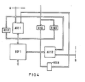
- a freely selectable sequence of the read image data can be achieved with a circuit supplement, the block diagram of which is shown in FIG. 4.
- This circuit is inserted at the locations marked A and B in FIG. It essentially consists of two address memories ADS1, ADS2, which are addressed with the respective states of the counters AZ1, AZ2 and to whose data outputs the address inputs of the image memory BSP1 are connected.
- the address memories ADS1, ADS2 are random memories Access that can be loaded via registers REG5, REG6 with addresses for the image memory BSP1 from the processor PR1.
- the image memory BSP1 can still be addressed directly by the counters AZ1, AZ2 via two registers REG7, REG8.
- the use of the two address memories ADS1, ADS2 allows the supplied counter readings, that is, if both counters count in the forward direction and the counter AZ2 is connected downstream of the counter AZ1, to change the coordinates of the measuring field in any way and thus to carry out any coordinate transformation.
- the counter reading modifications described above can also be carried out.
Landscapes
- Engineering & Computer Science (AREA)
- Theoretical Computer Science (AREA)
- Physics & Mathematics (AREA)
- General Physics & Mathematics (AREA)
- General Engineering & Computer Science (AREA)
- Mathematical Physics (AREA)
- Computer Hardware Design (AREA)
- Microelectronics & Electronic Packaging (AREA)
- Software Systems (AREA)
- Data Mining & Analysis (AREA)
- Databases & Information Systems (AREA)
- Image Processing (AREA)
- Image Analysis (AREA)
Applications Claiming Priority (2)
| Application Number | Priority Date | Filing Date | Title |
|---|---|---|---|
| DE19863620932 DE3620932A1 (de) | 1986-06-23 | 1986-06-23 | Anordnung zum verarbeiten von bilddaten |
| DE3620932 | 1986-06-23 |
Publications (1)
| Publication Number | Publication Date |
|---|---|
| EP0250976A1 true EP0250976A1 (fr) | 1988-01-07 |
Family
ID=6303482
Family Applications (1)
| Application Number | Title | Priority Date | Filing Date |
|---|---|---|---|
| EP87108479A Ceased EP0250976A1 (fr) | 1986-06-23 | 1987-06-12 | Dispositif de traitement de données d'images |
Country Status (2)
| Country | Link |
|---|---|
| EP (1) | EP0250976A1 (fr) |
| DE (1) | DE3620932A1 (fr) |
Cited By (2)
| Publication number | Priority date | Publication date | Assignee | Title |
|---|---|---|---|---|
| EP0411633A2 (fr) * | 1989-08-02 | 1991-02-06 | Fujitsu Limited | Circuit de commande de conversion de balayage comprenant des mÀ©moires et un générateur d'adresses pour générer un signal d'adresse en forme de zigzag vers les mémoires |
| FR2716276A1 (fr) * | 1994-02-16 | 1995-08-18 | Sgs Thomson Microelectronics | Circuit de réorganisation de données. |
Families Citing this family (1)
| Publication number | Priority date | Publication date | Assignee | Title |
|---|---|---|---|---|
| ES2007960A6 (es) * | 1988-07-12 | 1989-07-01 | Ona Electro Erosion | Sistema de generacion en dos dimensiones de la geometria de un modelo por medio de vision artificial. |
Citations (4)
| Publication number | Priority date | Publication date | Assignee | Title |
|---|---|---|---|---|
| US3976982A (en) * | 1975-05-12 | 1976-08-24 | International Business Machines Corporation | Apparatus for image manipulation |
| US4124871A (en) * | 1977-08-31 | 1978-11-07 | International Business Machines Corporation | Image data resolution change apparatus and process utilizing boundary compression coding of objects |
| US4168488A (en) * | 1977-09-12 | 1979-09-18 | International Business Machines Corporation | Image rotation apparatus |
| FR2574575A1 (fr) * | 1984-12-11 | 1986-06-13 | O Donnell Ciaran | Processeur de trace de vecteur |
-
1986
- 1986-06-23 DE DE19863620932 patent/DE3620932A1/de not_active Withdrawn
-
1987
- 1987-06-12 EP EP87108479A patent/EP0250976A1/fr not_active Ceased
Patent Citations (4)
| Publication number | Priority date | Publication date | Assignee | Title |
|---|---|---|---|---|
| US3976982A (en) * | 1975-05-12 | 1976-08-24 | International Business Machines Corporation | Apparatus for image manipulation |
| US4124871A (en) * | 1977-08-31 | 1978-11-07 | International Business Machines Corporation | Image data resolution change apparatus and process utilizing boundary compression coding of objects |
| US4168488A (en) * | 1977-09-12 | 1979-09-18 | International Business Machines Corporation | Image rotation apparatus |
| FR2574575A1 (fr) * | 1984-12-11 | 1986-06-13 | O Donnell Ciaran | Processeur de trace de vecteur |
Cited By (6)
| Publication number | Priority date | Publication date | Assignee | Title |
|---|---|---|---|---|
| EP0411633A2 (fr) * | 1989-08-02 | 1991-02-06 | Fujitsu Limited | Circuit de commande de conversion de balayage comprenant des mÀ©moires et un générateur d'adresses pour générer un signal d'adresse en forme de zigzag vers les mémoires |
| EP0411633A3 (en) * | 1989-08-02 | 1992-11-19 | Fujitsu Limited | Scan converter control circuit having memories and address generator for generating zigzag address signal supplied to the memories |
| US5313299A (en) * | 1989-08-02 | 1994-05-17 | Fujitsu Limited | Scan converter control circuit having memories and address generator for generating zigzag address signal supplied to the memories |
| FR2716276A1 (fr) * | 1994-02-16 | 1995-08-18 | Sgs Thomson Microelectronics | Circuit de réorganisation de données. |
| EP0668557A1 (fr) * | 1994-02-16 | 1995-08-23 | STMicroelectronics S.A. | Circuit de réorganisation de données |
| US5717899A (en) * | 1994-02-16 | 1998-02-10 | Sgs-Thomson Microelectronics S.A. | System for writing words into memory in first order and concurrently reading words from memory in second order based on input output ranks of words |
Also Published As
| Publication number | Publication date |
|---|---|
| DE3620932A1 (de) | 1988-01-07 |
Similar Documents
| Publication | Publication Date | Title |
|---|---|---|
| DE3305710C2 (de) | Schaltungsanordnung zur Merkmalserkennung bei auf einem Bildschirm darstellbaren Objekten | |
| DE3111027C2 (fr) | ||
| DE3688178T2 (de) | Verfahren zur Bildextraktion eines sich bewegenden Objekts. | |
| DE3419063C2 (fr) | ||
| EP0038411B1 (fr) | Dispositif de mémorisation et d'affichage de données graphiques | |
| DE68907383T2 (de) | Verfahren und Anordnung zur Umsetzung von Umrissdaten in Rasterdaten. | |
| DE3689926T2 (de) | Einrichtung zur sequenziellen Bildtransformation. | |
| DE69708871T2 (de) | Bildanzeigesysteme | |
| CH620542A5 (fr) | ||
| DE69225839T2 (de) | Filtersystem und Verfahren zur Bildverarbeitung mit sehr hoher Geschwindigkeit | |
| DE3751312T2 (de) | Verfahren und Einrichtung zur Verarbeitung von Bilddaten. | |
| DE3713627C2 (fr) | ||
| DE3038195A1 (de) | Vorrichtung zur verarbeitung von visueller information | |
| EP0625762A1 (fr) | Méthode de connexion de radiographies et dispositif de réalisation de la méthode | |
| DE69215155T2 (de) | Gerät mit schneller Kopierung zwischen Rasterpuffern in einem Anzeigesystem mit Doppel-Pufferspeichern | |
| DE3508606C2 (fr) | ||
| DE4425326C2 (de) | Bewegtbildanzeigevorrichtung | |
| DE3688132T2 (de) | Bildbehandlung. | |
| DE2461651C3 (de) | Zählvorrichtung zum Zählen von Mustern | |
| EP0250976A1 (fr) | Dispositif de traitement de données d'images | |
| DE2817341C2 (de) | Optisches Handlesegerät für die maschinelle Zeichenerkennung | |
| DE4103880C2 (de) | Bildverarbeitungsgerät und -verfahren | |
| DE68907085T2 (de) | Graphisches Videosystem mit einer graphischen Positionsmarke. | |
| DE2223257C3 (de) | Sichtanzeigeeinrichtung zum Ziehen von Linien auf einer Kathodenstrahlröhren-Sichtanzeigefläche | |
| DE69626246T2 (de) | Steuerschaltung für eine Flüssigkristallanzeige mit verbesserter Datenübertragung |
Legal Events
| Date | Code | Title | Description |
|---|---|---|---|
| PUAI | Public reference made under article 153(3) epc to a published international application that has entered the european phase |
Free format text: ORIGINAL CODE: 0009012 |
|
| AK | Designated contracting states |
Kind code of ref document: A1 Designated state(s): BE DE FR GB IT NL |
|
| 17P | Request for examination filed |
Effective date: 19880630 |
|
| 17Q | First examination report despatched |
Effective date: 19900404 |
|
| STAA | Information on the status of an ep patent application or granted ep patent |
Free format text: STATUS: THE APPLICATION HAS BEEN REFUSED |
|
| 18R | Application refused |
Effective date: 19920112 |
|
| RIN1 | Information on inventor provided before grant (corrected) |
Inventor name: KICK, HORST Inventor name: HELMA, HANS |