EP0248564A1 - Optical waveguides and their manufacture - Google Patents
Optical waveguides and their manufacture Download PDFInfo
- Publication number
- EP0248564A1 EP0248564A1 EP87304500A EP87304500A EP0248564A1 EP 0248564 A1 EP0248564 A1 EP 0248564A1 EP 87304500 A EP87304500 A EP 87304500A EP 87304500 A EP87304500 A EP 87304500A EP 0248564 A1 EP0248564 A1 EP 0248564A1
- Authority
- EP
- European Patent Office
- Prior art keywords
- fibre
- glass
- dopant
- semiconductor
- core
- Prior art date
- Legal status (The legal status is an assumption and is not a legal conclusion. Google has not performed a legal analysis and makes no representation as to the accuracy of the status listed.)
- Granted
Links
Images

Classifications
-
- G—PHYSICS
- G02—OPTICS
- G02F—OPTICAL DEVICES OR ARRANGEMENTS FOR THE CONTROL OF LIGHT BY MODIFICATION OF THE OPTICAL PROPERTIES OF THE MEDIA OF THE ELEMENTS INVOLVED THEREIN; NON-LINEAR OPTICS; FREQUENCY-CHANGING OF LIGHT; OPTICAL LOGIC ELEMENTS; OPTICAL ANALOGUE/DIGITAL CONVERTERS
- G02F1/00—Devices or arrangements for the control of the intensity, colour, phase, polarisation or direction of light arriving from an independent light source, e.g. switching, gating or modulating; Non-linear optics
- G02F1/35—Non-linear optics
- G02F1/365—Non-linear optics in an optical waveguide structure
-
- C—CHEMISTRY; METALLURGY
- C03—GLASS; MINERAL OR SLAG WOOL
- C03B—MANUFACTURE, SHAPING, OR SUPPLEMENTARY PROCESSES
- C03B37/00—Manufacture or treatment of flakes, fibres, or filaments from softened glass, minerals, or slags
- C03B37/01—Manufacture of glass fibres or filaments
- C03B37/012—Manufacture of preforms for drawing fibres or filaments
- C03B37/01205—Manufacture of preforms for drawing fibres or filaments starting from tubes, rods, fibres or filaments
- C03B37/01211—Manufacture of preforms for drawing fibres or filaments starting from tubes, rods, fibres or filaments by inserting one or more rods or tubes into a tube
-
- C—CHEMISTRY; METALLURGY
- C03—GLASS; MINERAL OR SLAG WOOL
- C03B—MANUFACTURE, SHAPING, OR SUPPLEMENTARY PROCESSES
- C03B37/00—Manufacture or treatment of flakes, fibres, or filaments from softened glass, minerals, or slags
- C03B37/01—Manufacture of glass fibres or filaments
- C03B37/012—Manufacture of preforms for drawing fibres or filaments
- C03B37/01265—Manufacture of preforms for drawing fibres or filaments starting entirely or partially from molten glass, e.g. by dipping a preform in a melt
- C03B37/01274—Manufacture of preforms for drawing fibres or filaments starting entirely or partially from molten glass, e.g. by dipping a preform in a melt by extrusion or drawing
-
- C—CHEMISTRY; METALLURGY
- C03—GLASS; MINERAL OR SLAG WOOL
- C03C—CHEMICAL COMPOSITION OF GLASSES, GLAZES OR VITREOUS ENAMELS; SURFACE TREATMENT OF GLASS; SURFACE TREATMENT OF FIBRES OR FILAMENTS MADE FROM GLASS, MINERALS OR SLAGS; JOINING GLASS TO GLASS OR OTHER MATERIALS
- C03C13/00—Fibre or filament compositions
- C03C13/04—Fibre optics, e.g. core and clad fibre compositions
-
- C—CHEMISTRY; METALLURGY
- C03—GLASS; MINERAL OR SLAG WOOL
- C03C—CHEMICAL COMPOSITION OF GLASSES, GLAZES OR VITREOUS ENAMELS; SURFACE TREATMENT OF GLASS; SURFACE TREATMENT OF FIBRES OR FILAMENTS MADE FROM GLASS, MINERALS OR SLAGS; JOINING GLASS TO GLASS OR OTHER MATERIALS
- C03C3/00—Glass compositions
- C03C3/32—Non-oxide glass compositions, e.g. binary or ternary halides, sulfides or nitrides of germanium, selenium or tellurium
- C03C3/321—Chalcogenide glasses, e.g. containing S, Se, Te
-
- G—PHYSICS
- G02—OPTICS
- G02B—OPTICAL ELEMENTS, SYSTEMS OR APPARATUS
- G02B6/00—Light guides; Structural details of arrangements comprising light guides and other optical elements, e.g. couplings
- G02B6/02—Optical fibres with cladding with or without a coating
-
- G—PHYSICS
- G02—OPTICS
- G02F—OPTICAL DEVICES OR ARRANGEMENTS FOR THE CONTROL OF LIGHT BY MODIFICATION OF THE OPTICAL PROPERTIES OF THE MEDIA OF THE ELEMENTS INVOLVED THEREIN; NON-LINEAR OPTICS; FREQUENCY-CHANGING OF LIGHT; OPTICAL LOGIC ELEMENTS; OPTICAL ANALOGUE/DIGITAL CONVERTERS
- G02F1/00—Devices or arrangements for the control of the intensity, colour, phase, polarisation or direction of light arriving from an independent light source, e.g. switching, gating or modulating; Non-linear optics
- G02F1/35—Non-linear optics
- G02F1/355—Non-linear optics characterised by the materials used
- G02F1/3551—Crystals
-
- C—CHEMISTRY; METALLURGY
- C03—GLASS; MINERAL OR SLAG WOOL
- C03B—MANUFACTURE, SHAPING, OR SUPPLEMENTARY PROCESSES
- C03B2201/00—Type of glass produced
- C03B2201/06—Doped silica-based glasses
- C03B2201/30—Doped silica-based glasses doped with metals, e.g. Ga, Sn, Sb, Pb or Bi
-
- C—CHEMISTRY; METALLURGY
- C03—GLASS; MINERAL OR SLAG WOOL
- C03B—MANUFACTURE, SHAPING, OR SUPPLEMENTARY PROCESSES
- C03B2201/00—Type of glass produced
- C03B2201/06—Doped silica-based glasses
- C03B2201/30—Doped silica-based glasses doped with metals, e.g. Ga, Sn, Sb, Pb or Bi
- C03B2201/40—Doped silica-based glasses doped with metals, e.g. Ga, Sn, Sb, Pb or Bi doped with transition metals other than rare earth metals, e.g. Zr, Nb, Ta or Zn
-
- C—CHEMISTRY; METALLURGY
- C03—GLASS; MINERAL OR SLAG WOOL
- C03B—MANUFACTURE, SHAPING, OR SUPPLEMENTARY PROCESSES
- C03B2205/00—Fibre drawing or extruding details
- C03B2205/02—Upward drawing
Definitions
- This invention relates to a method of preparing optical wave guiding structures, eg multimode and monomode glass fibres. At least a selected portion of the structure contains a dopant, eg a semiconductor, in colloidal form.
- a dopant eg a semiconductor
- the structures which contain colloidal semiconductors have a refractive index which is intensity dependent.
- semiconductor doped glasses have been examined for non-linear properties. These materials consist of oxide glasses in which semiconductor crystallites are dispersed and these glasses are available as optical filters. The band gap and dimensions of the dispersed semiconductor crystallites determines the cut-off wave length of the filter. This can be varied by suitable choice of the semiconductor, and processing conditions. Ironside et al, in a paper "Wave guide fabrication in non-linear semiconductor glasses” ECOC 85 (Venice) especially at page 237, have proposed to make planar wave-guiding structures by ion-exchange with suitable glasses of this type.
- This invention comprises a glass optical fibre, eg a monomode fibre, wherein either the core or the cladding or both core and cladding take the form of a continuous glass phase having dispersed therein colloidal particles of a semiconductor, eg a semiconductor having a band gap of 3.8 to O.27 ev, especially 2.5 to 1.4 ev.
- the colloidal particles preferably have sizes in the range 1 to 1OOOnm.
- Suitable semiconductors include wherein w, x, y, a and b are O to 1 inclusive.
- the invention also comprises devices which include a fibre according to the invention.
- Such devices preferably comprise an un-jointed length of fibre having at least one active region and at least one passive region wherein, in the or each passive region, the semiconductor is dissolved in the glass continuous phase and, in the or each active region, the semiconductor is colloidally dispersed.
- This preferred form confines the non-linear activity to the region(s) where it is desired, ie to the active region(s) where the particles are present. It also avoids losses because there are no joints between the active region(s) and the feeder(s).
- the fibres according to the invention are fabricated by the conventional drawing of a preform which contains the semiconductor either dispersed or dissolved. If the semiconductor is dissolved, or if it dissolves during processing, the nit is necessary to precipitate it as a colloid in the final fibre. This precipitation may be achieved by:-
- the treatment is applied only to the active region or regions.
- Some of the semiconductor dopants which are used in the invention are well known as colourants for glass and, in particular, as additives for filter glasses which have a well defined cut-off wave length. (Some semiconductors, eg those having band gaps of O.27 to O.4 ev such as PbSe and PbS have cut-offs at wavelengths in the region of 3 ⁇ m and these appear black to the eye).
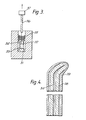
- the preform comprises a rod 11 which is situated in the bore of a tubular member 1O.
- the tubular member 1O has an enlarged portion 12 which functions as a handle during processing.
- the rod 11 has a head 13 which can be accommodated in the enlarged portion 12 but which prevents the rod 11 entering too far into the tube 1O during drawing.
- the rod 11 and the inner face of the tube 1O are mechanically polished to facilitate fusion.
- the assembly can be heated to drawing temperature (which causes the tube 11 to shrink onto the rod 1O) and drawn into fibre.
- Figure 2 shows a modification in which there is an outer tube 2O which serves to provide a protective layer during processing and also in the final product.
- the basic mechanics are conventional, eg the "rod-in-tube" process.
- either the tube 1O or rod 11 contains the dopant which is either (a) retained as a colloid throughout or (b) dissolved eg to give a solid phase supersaturated solution in the fibre.
- At least portions of said fibre are treated, eg for a suitable time at a suitable temperature, so as to cause some (or all) of the dissolved dopant to precipitate as a colloid.
- any dopant which remains dissolved has little or no effect on the useful properties.
- it is important to precipitate enough of the dopant there is no need to precipitate all of it. For convenience some will usually be left in solution.
- the three-layer version of Figure 2 is particularly appropriate for doped cladding.
- Tube 1O has a bore diameter of 4.5mm and 7mm outer diameter formed of a sodium/calcium silicate glass. It was bought from Gallenkamp Ltd.
- Rod 11 has a diameter of 3mm and it was formed of Schott filter glass OG 53O which is a potassium/zinc silicate glass doped with colloidal cadmium sulphoselenide. Since rod 11 has a diameter of 3mm and the bore of tube 1O a diameter of 4.5mm there is an annulus about 75O ⁇ m.
- This assembly was heated to about 1OOO°C (at which temperature both rod 11 and tube 1O became very fluid). This caused tube 1O to shrink onto rod 11 and it also caused the colloidal dopant to dissolve.
- the hot-work was drawn by hand to fibre of total diameter 25O ⁇ m with a core of 15O ⁇ m diameter.
- the transmission properties of the fibre were compared with the transmission properties of the untreated rod.
- the rod acted as a filter with a cut-off at short wave lengths (note this is the commercial purpose of filter glass OG 53O) but the drawn fibre did not. This indicates that the colloidal particles had dissolved (which destroys the filtering effect and the non-linear effect).
- the fibre also had a high transparency which confirms the lack of particles.
- the core consists of a supersaturated (solid) solution of the semiconductor in the glass phase.
- the yellow colour typical of the filter re-appeared implying that the semiconductor had re-precipitated.
- Fibre with a dopant in the cladding can also be made but using the three-layer structure illustrated in Figure 2. This would result in a fibre with an outer layer which protects the fibre during the re-precipitation of the colloid. Fibre with a semiconductor colloid in the cladding is particularly useful for making intensity dependent switches.
- the source glass used in this example was Hoya filter glass H 64O which is a sodium/potassium/zinc silicate glass which contains about O.5 to 1 weight % of colloidal cadmium sulphoselenide.
- the melt 33 was contained in a platinum/gold crucible 32 which stands on a support block 31.
- a cooling coil 35 is located above the mouth of crucible 32.
- the height of the colling coil 35, ie its height above the crucible 32 is adjustable by means not shown.
- Figure 3 shows a silica rod 34 which is in the course of production.
- the rod 34 is attached to the end of a silica bar 36 which is held in movable clamp 37.
- the cross section of bar 36 is small enough so that it can be inserted into the crucible 33 via cooling coil 35.
- the method of preparing rod 34 is as follows:
- the melt 33 in the crucible 32 contains the semiconductor in the dissolved state.
- the bar 36 is lowered through cooling coil 35 until it just touches the surface of the melt 33.
- melt 33 adheres and, therefore, a portion of the melt is drawn upwards.
- the cooling coil 35 reduced the temperature of this portion so that it cools to a solid rod.
- the temperature of the solid rod is not high enough to prevent precipitation of the dissolved semiconductor. Thus it contains a supersaturated solution of the semiconductor.
- the diameter of the rod 34 is controlled by:
- Figure 4 shows a rod 34, prepared as described above, located in the bore of a capillary tube 38 which is contained inside an outer sleeve 39. At its top end the assembly is bent and fused so that its components are secured together. The length of the assembly was about 1m.
- rod 34 is made of a potassium/zinc silicate glass which contains dissolved cadmium sulphoselenide. Its diameter is O.1mm.
- Capillary 38 is made of sodium-calcium silicate glass. Its outer diameter is 6.Omm and its bore diameter is 1.5mm.
- Sleeve 39 is made of sodium calcium silicate glass. Its outer diameter is 1Omm and its bore diameter is 8.Omm.
- absorption cut-offs are given below in tables I and II. Absorption measurements were made on lengths of fibre 1Omm long. The fibre transmits at higher wavelengths and it becomes strongly absorbent at lower wavelengths.
- the cut-off is specified as two values, ie in the form A/B.
- A is the (longer) wavelength in nm at which attenuation becomes noticeable.
- B is the (shorter) wavelength in nm at which attenuation is approximately 2OdB.
- the notation "A/B" indicates the location and sharpness of the cut-off edge.
- Samples of the assembly shown in Figure 4 were also drawn into fibre at lower temperatures, eg 95O°C. At these lower temperatures the semiconductor was precipitated as a colloid.
- the rate of drawing was 8mm/min for the preform and 3Om.min for the fibre, giving a fibre with diameter of O.16mm.
- the size of the colloidal particles of the semiconductor was about 2O to 3Onm.
- double crucible The well known technique called "double crucible” is also applicable to making fibre according to the invention.
- This technique uses concentric crucibles which contain molten glass, ie one crucible for each region of the fibre.
- the crucibles are associated with a concentric die and the fibre structure is drawn directly from the melt.
- the crucibles may be continuously recharged during drawing, eg by lowering rods into the melts to maintain a constant level.
- the fibre drawing can be carried out using doped, preferably semiconductor doped, glass in one or more of the crucibles.
- dopant dissolves and the drawing is carried out under such conditions that the dopant remains in solution, ie fibre containing a supersaturated solution of dopant is produced. (Keeping the dopant in solution is achieved provided that the rate of cooling of the fibre is kept fast enough).
Landscapes
- Physics & Mathematics (AREA)
- Chemical & Material Sciences (AREA)
- Nonlinear Science (AREA)
- Engineering & Computer Science (AREA)
- Optics & Photonics (AREA)
- Life Sciences & Earth Sciences (AREA)
- Geochemistry & Mineralogy (AREA)
- Materials Engineering (AREA)
- Organic Chemistry (AREA)
- General Physics & Mathematics (AREA)
- General Chemical & Material Sciences (AREA)
- Chemical Kinetics & Catalysis (AREA)
- General Life Sciences & Earth Sciences (AREA)
- Manufacturing & Machinery (AREA)
- Crystallography & Structural Chemistry (AREA)
- Glass Compositions (AREA)
- Optical Integrated Circuits (AREA)
- Optical Couplings Of Light Guides (AREA)
Abstract
Description
- This invention relates to a method of preparing optical wave guiding structures, eg multimode and monomode glass fibres. At least a selected portion of the structure contains a dopant, eg a semiconductor, in colloidal form.
- The structures which contain colloidal semiconductors have a refractive index which is intensity dependent.
- It is known that semiconductor materials, eg cadmium sulphide which possesses a large third order susceptibility, have a refractive index which is dependent on the intensity of incident radiation. It has been proposed to utilise this property in the broad field of optical signal processing, eg as bistable elements and optical power dependent switches.
- Recently a class of materials known as semiconductor doped glasses have been examined for non-linear properties. These materials consist of oxide glasses in which semiconductor crystallites are dispersed and these glasses are available as optical filters. The band gap and dimensions of the dispersed semiconductor crystallites determines the cut-off wave length of the filter. This can be varied by suitable choice of the semiconductor, and processing conditions. Ironside et al, in a paper "Wave guide fabrication in non-linear semiconductor glasses" ECOC 85 (Venice) especially at page 237, have proposed to make planar wave-guiding structures by ion-exchange with suitable glasses of this type.
- Patela et al, in Electronics Letters of 1O April 1986, Vol. 22, No. 8 at pages 411 and 412 consider the fabrication and properties of a non-linear wave guiding structure consisting of a thin film of Corning 7O59 glass deposited on the surface of CdSxSe1-x doped glass. Abashkin et al, in Soviet Journal of Quantum Electronics, Vol. 12 (1982) October, No. 1O, published in New York, USA, at pages 1343 to 1345 discuss the propagation of light in chalcogenide semiconductor fibres.
- This invention comprises a glass optical fibre, eg a monomode fibre, wherein either the core or the cladding or both core and cladding take the form of a continuous glass phase having dispersed therein colloidal particles of a semiconductor, eg a semiconductor having a band gap of 3.8 to O.27 ev, especially 2.5 to 1.4 ev. The colloidal particles preferably have sizes in the range 1 to 1OOOnm.
- Examples of suitable semiconductors include

- The invention also comprises devices which include a fibre according to the invention. Such devices preferably comprise an un-jointed length of fibre having at least one active region and at least one passive region wherein, in the or each passive region, the semiconductor is dissolved in the glass continuous phase and, in the or each active region, the semiconductor is colloidally dispersed. This preferred form confines the non-linear activity to the region(s) where it is desired, ie to the active region(s) where the particles are present. It also avoids losses because there are no joints between the active region(s) and the feeder(s).
- The fibres according to the invention are fabricated by the conventional drawing of a preform which contains the semiconductor either dispersed or dissolved. If the semiconductor is dissolved, or if it dissolves during processing, the nit is necessary to precipitate it as a colloid in the final fibre. This precipitation may be achieved by:-
- (a) heat treatment, eg relatively short periods at high temperature or longer periods at low temperatures such as 1 minute at 7OO°C or 3O minutes at 6OO°C;
- (b) laser initiation at wave lengths where the most glass absorbs, eg UV and IR;
- (c) electron beam treatment;
- (d) ion bombardment.
- When the final product contains active and passive regions the treatment is applied only to the active region or regions.
- Some of the semiconductor dopants which are used in the invention are well known as colourants for glass and, in particular, as additives for filter glasses which have a well defined cut-off wave length. (Some semiconductors, eg those having band gaps of O.27 to O.4 ev such as PbSe and PbS have cut-offs at wavelengths in the region of 3µm and these appear black to the eye).
- Preparations according to the invention will now be described by way of example with reference to the accompanying drawings in which:-
- Figure 1 illustrates a two-layer preform for making an optical fibre having a core and a cladding;
- Figure 2 illustrates a three-layer preform for making an optical fibre in which the core and cladding are protected by a third outer-layer; and
- Figures 3 and 4 illustrate a variant of Figures 1 and 2.
- As shown in Figure 1, the preform comprises a rod 11 which is situated in the bore of a tubular member 1O. The tubular member 1O has an enlarged
portion 12 which functions as a handle during processing. The rod 11 has ahead 13 which can be accommodated in the enlargedportion 12 but which prevents the rod 11 entering too far into the tube 1O during drawing. The rod 11 and the inner face of the tube 1O are mechanically polished to facilitate fusion. There is a small annulus, eg about 2OO to 8OOµm, between rod 11 and tube 1O so that the rod slides easily into the tube. The assembly can be heated to drawing temperature (which causes the tube 11 to shrink onto the rod 1O) and drawn into fibre. - Figure 2 shows a modification in which there is an outer tube 2O which serves to provide a protective layer during processing and also in the final product.
- It will be appreciated that the basic mechanics are conventional, eg the "rod-in-tube" process. However, either the tube 1O or rod 11 contains the dopant which is either (a) retained as a colloid throughout or (b) dissolved eg to give a solid phase supersaturated solution in the fibre. At least portions of said fibre are treated, eg for a suitable time at a suitable temperature, so as to cause some (or all) of the dissolved dopant to precipitate as a colloid. It should be noted that any dopant which remains dissolved has little or no effect on the useful properties. Thus, while it is important to precipitate enough of the dopant, there is no need to precipitate all of it. For convenience some will usually be left in solution. The three-layer version of Figure 2 is particularly appropriate for doped cladding.
- Three specific embodiments of the invention will now be described by way of example.
- Tube 1O has a bore diameter of 4.5mm and 7mm outer diameter formed of a sodium/calcium silicate glass. It was bought from Gallenkamp Ltd.
- Rod 11 has a diameter of 3mm and it was formed of Schott filter glass OG 53O which is a potassium/zinc silicate glass doped with colloidal cadmium sulphoselenide. Since rod 11 has a diameter of 3mm and the bore of tube 1O a diameter of 4.5mm there is an annulus about 75Oµm.
- This assembly was heated to about 1OOO°C (at which temperature both rod 11 and tube 1O became very fluid). This caused tube 1O to shrink onto rod 11 and it also caused the colloidal dopant to dissolve. The hot-work was drawn by hand to fibre of total diameter 25Oµm with a core of 15Oµm diameter.
- The transmission properties of the fibre were compared with the transmission properties of the untreated rod. The rod acted as a filter with a cut-off at short wave lengths (note this is the commercial purpose of filter glass OG 53O) but the drawn fibre did not. This indicates that the colloidal particles had dissolved (which destroys the filtering effect and the non-linear effect). The fibre also had a high transparency which confirms the lack of particles. In other words, the core consists of a supersaturated (solid) solution of the semiconductor in the glass phase.
- A portion of the clear drawn fibre, ie a portion 1Omm in length, was heated to approximately 7OO°C for approximately 1 minute. The yellow colour typical of the filter re-appeared implying that the semiconductor had re-precipitated. A transmission spectrum of the fibre was plotted and the plot showed a cut-off typical of the colloidal filter. This also implies that the semiconductor had re-precipitated as a colloid. (As an alternative the semiconductor was re-precipitated by heating a (different) segment for 3O minutes at 6OO°C).
- This example replicates Example 1 but the assembly was only heated to about 72O°C (instead of 1OOO°C). At this lower temperature the colloidal dopant did not dissolve although its particle size increased slightly. There was, therefore, no need to re-precipitate the dopant.
- Fibre with a dopant in the cladding can also be made but using the three-layer structure illustrated in Figure 2. This would result in a fibre with an outer layer which protects the fibre during the re-precipitation of the colloid. Fibre with a semiconductor colloid in the cladding is particularly useful for making intensity dependent switches.
- The source glass used in this example was Hoya filter glass H 64O which is a sodium/potassium/zinc silicate glass which contains about O.5 to 1 weight % of colloidal cadmium sulphoselenide.
- A suitable quantity of H 64O, shown as
melt 33 in Figure 3, was melted at approximately 1O5O°C in a furnace 3O. Themelt 33 was contained in a platinum/gold crucible 32 which stands on asupport block 31. A cooling coil 35 is located above the mouth ofcrucible 32. The height of the colling coil 35, ie its height above thecrucible 32 is adjustable by means not shown. Figure 3 shows asilica rod 34 which is in the course of production. Therod 34 is attached to the end of asilica bar 36 which is held inmovable clamp 37. The cross section ofbar 36 is small enough so that it can be inserted into thecrucible 33 via cooling coil 35. - It will be appreciated that the following adjustments tend to favour thicker rods (and the inverse adjustments favour thinner rods):-
- (1) A lower furnace temperature giving a more viscous melt.
- (2) A smaller distance between the cooling coil 35 and the
melt 33 giving less chance for pulled melt to return to the crucible, and - (3) The speed of pulling, eg 5O to 2OO mm/sec.
- The method of preparing
rod 34 is as follows: - The
melt 33 in thecrucible 32 contains the semiconductor in the dissolved state. To start production of therod 34, thebar 36 is lowered through cooling coil 35 until it just touches the surface of themelt 33. On withdrawing therod 34 at a controlled rate, melt 33 adheres and, therefore, a portion of the melt is drawn upwards. The cooling coil 35 reduced the temperature of this portion so that it cools to a solid rod. However, the temperature of the solid rod is not high enough to prevent precipitation of the dissolved semiconductor. Thus it contains a supersaturated solution of the semiconductor. - The diameter of the
rod 34 is controlled by: - (1) The temperature of furnace 3O, approximately 1O5O C. °
- (2) The distance between the cooling coil 35 and the surface of the
melt 33, eg 5O to 15Omm. - Using the technique described above, we have prepared rods with diameters of O.2mm to 2mm.
- Figure 4 shows a
rod 34, prepared as described above, located in the bore of acapillary tube 38 which is contained inside anouter sleeve 39. At its top end the assembly is bent and fused so that its components are secured together. The length of the assembly was about 1m. - As implied above,
rod 34 is made of a potassium/zinc silicate glass which contains dissolved cadmium sulphoselenide. Its diameter is O.1mm. -
Capillary 38 is made of sodium-calcium silicate glass. Its outer diameter is 6.Omm and its bore diameter is 1.5mm. -
Sleeve 39 is made of sodium calcium silicate glass. Its outer diameter is 1Omm and its bore diameter is 8.Omm. - Using a conventional furnace (model TF 685 made by Severn Science) at 1O8O°C, the assembly of Figure 4 was drawn into optical wave-guiding fibre. In a set of experiments fibres with diameters in the range O.O8mm to O.15mm were prepared. The drawing temperature of 1O8O°C was chosen so that the semiconductor remained in supersaturated solution, ie "clear" fibre was produced.
- The reduction of diameter, namely 1Omm for the outer sleeve tube to values in the range O.O8mm to O.15mm, implies that the length must be stretched about 4,OOO to 16,OOO times. These draw ratios are conveniently produced by feeding the assembly at a rate of 2 to 2Omm/min and pulling fibre at a rate of 1O to 6Om/min.
- After drawing the fibre was heated at 6OO°C for 3O minutes. This precipitated the semiconductor as a colloid.
- Specific examples of absorption cut-offs are given below in tables I and II. Absorption measurements were made on lengths of fibre 1Omm long. The fibre transmits at higher wavelengths and it becomes strongly absorbent at lower wavelengths.
- The cut-off is specified as two values, ie in the form A/B. A is the (longer) wavelength in nm at which attenuation becomes noticeable. B is the (shorter) wavelength in nm at which attenuation is approximately 2OdB.
- The notation "A/B" indicates the location and sharpness of the cut-off edge.
- Three samples of glass fibre were heated for / minutes each at the temperature specified in Table I, and (when cold) the cut-offs were measured.

- In a second set of experiments three samples were all heated at 64O°C each for the time stated in Table II. Cut-offs were measured when cold.

- It can be seen that high temperatures and longer times move the cut-off to longer wavelengths, ie radiation having less energetic quanta. It is believed that this observation can be explained as follows. Higher temperatures and longer times both tend to grow larger colloidal particles and the smaller particles have larger band-gaps (known as quantum size effects) which correspond to attenuation at shorter wavelengths. (It is difficult to measure the size of the colloidal particles but this is believed to be about 2Onm).
- Samples of the assembly shown in Figure 4 were also drawn into fibre at lower temperatures, eg 95O°C. At these lower temperatures the semiconductor was precipitated as a colloid. The rate of drawing was 8mm/min for the preform and 3Om.min for the fibre, giving a fibre with diameter of O.16mm. The size of the colloidal particles of the semiconductor was about 2O to 3Onm.
- The well known technique called "double crucible" is also applicable to making fibre according to the invention. This technique uses concentric crucibles which contain molten glass, ie one crucible for each region of the fibre. The crucibles are associated with a concentric die and the fibre structure is drawn directly from the melt. The crucibles may be continuously recharged during drawing, eg by lowering rods into the melts to maintain a constant level.
- The fibre drawing can be carried out using doped, preferably semiconductor doped, glass in one or more of the crucibles. In the melt the dopant dissolves and the drawing is carried out under such conditions that the dopant remains in solution, ie fibre containing a supersaturated solution of dopant is produced. (Keeping the dopant in solution is achieved provided that the rate of cooling of the fibre is kept fast enough).
- Thus conventional double crucible techniques are used to provide fibre which contains a supersaturated solution of dopant in either or both the core and the cladding. As described above, the dopant is precipitated, either in the whole or selected portions of the fibre.
- The examples specifically described the precipitation of cadmium sulphoselenide semiconductors. Other materials, eg gold, can be precipitated according to the invention. As the specialist compositions of this invention form only a small portion of a transmission system there is wide flexibility to select the host glass for its properties as a solvent for the dopant.
Claims (20)

Applications Claiming Priority (4)
| Application Number | Priority Date | Filing Date | Title |
|---|---|---|---|
| GB868613525A GB8613525D0 (en) | 1986-06-04 | 1986-06-04 | Optical fibres |
| GB8613525 | 1986-06-04 | ||
| GB878706461A GB8706461D0 (en) | 1987-03-18 | 1987-03-18 | Optical waveguides |
| GB8706461 | 1987-03-18 |
Publications (2)
| Publication Number | Publication Date |
|---|---|
| EP0248564A1 true EP0248564A1 (en) | 1987-12-09 |
| EP0248564B1 EP0248564B1 (en) | 1994-10-26 |
Family
ID=26290855
Family Applications (1)
| Application Number | Title | Priority Date | Filing Date |
|---|---|---|---|
| EP87304500A Expired - Lifetime EP0248564B1 (en) | 1986-06-04 | 1987-05-20 | Optical waveguides and their manufacture |
Country Status (6)
| Country | Link |
|---|---|
| US (1) | US4974933A (en) |
| EP (1) | EP0248564B1 (en) |
| AT (1) | ATE113395T1 (en) |
| CA (1) | CA1294802C (en) |
| DE (1) | DE3750686T2 (en) |
| ES (1) | ES2062980T3 (en) |
Cited By (7)
| Publication number | Priority date | Publication date | Assignee | Title |
|---|---|---|---|---|
| GB2220079A (en) * | 1988-06-21 | 1989-12-28 | Stc Plc | Optically controlled optical power divider |
| GB2241348A (en) * | 1990-02-20 | 1991-08-28 | British Telecomm | Optical modulator |
| US5122178A (en) * | 1989-07-31 | 1992-06-16 | Hoya Corporation | Process for producing glass doped with dispersed microcrystallites |
| EP0466810A4 (en) * | 1989-04-04 | 1992-07-15 | Meyer H. Birnboim | Nonlinear optical materials |
| EP0716048A1 (en) * | 1994-12-01 | 1996-06-12 | AT&T Corp. | Method and apparatus for making optical fiber preforms and optical fibers fabricated therefrom |
| WO2002074708A1 (en) * | 2001-03-16 | 2002-09-26 | Optonest Corporation | Fabricating an optical fiber preform using mcvd |
| CN106495090A (en) * | 2016-11-24 | 2017-03-15 | 天津城建大学 | The method that conical fiber surface prepares colloid monolayer spherical array array structure |
Families Citing this family (9)
| Publication number | Priority date | Publication date | Assignee | Title |
|---|---|---|---|---|
| US5117472A (en) * | 1990-12-28 | 1992-05-26 | At&T Bell Laboratories | Optical coupler with mode-mixing refractive microparticles |
| US6241819B1 (en) * | 1993-04-20 | 2001-06-05 | North American Philips Corp. | Method of manufacturing quantum sized doped semiconductor particles |
| US5948196A (en) * | 1995-08-09 | 1999-09-07 | Owens Corning Fiberglas Technology, Inc. | Layered ceramic reinforcing fibers for use in composites |
| FR2839063B1 (en) * | 2002-04-29 | 2005-01-07 | Cit Alcatel | PROCESS FOR PRODUCING OPTICAL FIBER PREFORMS |
| DE10331103B4 (en) * | 2002-07-04 | 2008-06-26 | Schott Ag | Double crucible for glass drawing process and method for producing glass fibers or associated preforms with the double crucible |
| US7455476B2 (en) * | 2003-12-18 | 2008-11-25 | Kmc Enterprises, Inc. | Method of reconstructing a bituminous-surfaced pavement |
| US9952719B2 (en) | 2012-05-24 | 2018-04-24 | Corning Incorporated | Waveguide-based touch system employing interference effects |
| US20140210770A1 (en) | 2012-10-04 | 2014-07-31 | Corning Incorporated | Pressure sensing touch systems and methods |
| US9134842B2 (en) * | 2012-10-04 | 2015-09-15 | Corning Incorporated | Pressure sensing touch systems and methods |
Citations (2)
| Publication number | Priority date | Publication date | Assignee | Title |
|---|---|---|---|---|
| US3571737A (en) * | 1968-06-07 | 1971-03-23 | Bell Telephone Labor Inc | Transmission line |
| US4283213A (en) * | 1979-10-22 | 1981-08-11 | International Telephone And Telegraph Corporation | Method of fabrication of single mode optical fibers or waveguides |
Family Cites Families (27)
| Publication number | Priority date | Publication date | Assignee | Title |
|---|---|---|---|---|
| US3254031A (en) * | 1962-06-27 | 1966-05-31 | Eastman Kodak Co | Borate glass for laser use |
| DE1928947A1 (en) * | 1968-06-29 | 1970-01-02 | Philips Nv | Glass for a fiber optic element |
| US3894857A (en) * | 1968-07-06 | 1975-07-15 | Nippon Selfoc Co Ltd | Process for exchanging alkali ions for thallium ions in a glass fiber |
| US3599106A (en) * | 1968-11-06 | 1971-08-10 | American Optical Corp | High intensity-high coherence laser system |
| US3636473A (en) * | 1969-03-06 | 1972-01-18 | American Optical Corp | Composite glass laser rod |
| US3808549A (en) * | 1972-03-30 | 1974-04-30 | Corning Glass Works | Optical waveguide light source |
| US3785834A (en) * | 1972-06-09 | 1974-01-15 | Owens Illinois Inc | Glasses,glass-ceramics and process for making same |
| US3938974A (en) * | 1973-04-27 | 1976-02-17 | Macedo Pedro B | Method of producing optical wave guide fibers |
| FR2238679B1 (en) * | 1973-07-26 | 1978-06-30 | Auzel Francois | |
| US3864113A (en) * | 1973-10-19 | 1975-02-04 | Corning Glass Works | Method of Producing Glass by Flame Hydrolysis |
| US4040890A (en) * | 1975-06-27 | 1977-08-09 | Bell Telephone Laboratories, Incorporated | Neodymium oxide doped yttrium aluminum garnet optical fiber |
| US3971645A (en) * | 1975-09-12 | 1976-07-27 | Bell Telephone Laboratories, Incorporated | Method of making compound-glass optical waveguides fabricated by a metal evaporation technique |
| US4149772A (en) * | 1975-09-22 | 1979-04-17 | Northern Electric Company Limited | Optical fibre having low mode dispersion |
| FR2339266A1 (en) * | 1976-01-26 | 1977-08-19 | Commissariat Energie Atomique | Multi-layer light amplifying system - has glass amplifying medium with active centres of trivalent ions of neodymium increasing in concentration away from optical pump |
| DE7706786U1 (en) * | 1977-03-05 | 1977-06-08 | Jenaer Glaswerk Schott & Gen., 6500 Mainz | FIBER OPTIC WITH CROSS-LIGHT |
| US4422719A (en) * | 1981-05-07 | 1983-12-27 | Space-Lyte International, Inc. | Optical distribution system including light guide |
| US4419115A (en) * | 1981-07-31 | 1983-12-06 | Bell Telephone Laboratories, Incorporated | Fabrication of sintered high-silica glasses |
| US4715679A (en) * | 1981-12-07 | 1987-12-29 | Corning Glass Works | Low dispersion, low-loss single-mode optical waveguide |
| US4516826A (en) * | 1983-04-21 | 1985-05-14 | At&T Technologies, Inc. | Single mode lightguide fiber having a trapezoidal refractive index profile |
| US4618211A (en) * | 1984-03-12 | 1986-10-21 | At&T Bell Laboratories | Optical fiber tap with activatable chemical species |
| US4637025A (en) * | 1984-10-22 | 1987-01-13 | Polaroid Corporation | Super radiant light source |
| US4597787A (en) * | 1984-11-13 | 1986-07-01 | Ispra Fibroptics Industries Herzlia Ltd. | Manufacture of optical fibre preforms |
| JPS62502748A (en) * | 1985-06-03 | 1987-10-22 | ヒユ−ズ・エアクラフト・カンパニ− | How to introduce dovants into optical fiber preforms |
| US4780877A (en) * | 1985-07-26 | 1988-10-25 | Polaroid Corporation | Optical fiber laser |
| AU584739B2 (en) * | 1985-08-13 | 1989-06-01 | British Technology Group Limited | Optical fibres |
| US4666486A (en) * | 1985-09-24 | 1987-05-19 | Hutta Joseph J | Process for making bulk heavy metal fluoride glasses |
| JPS62158135A (en) * | 1985-12-28 | 1987-07-14 | Hoya Corp | Single mode optical fiber having faraday rotation effect |
-
1987
- 1987-05-19 CA CA000537388A patent/CA1294802C/en not_active Expired - Lifetime
- 1987-05-20 ES ES87304500T patent/ES2062980T3/en not_active Expired - Lifetime
- 1987-05-20 DE DE3750686T patent/DE3750686T2/en not_active Expired - Lifetime
- 1987-05-20 EP EP87304500A patent/EP0248564B1/en not_active Expired - Lifetime
- 1987-05-20 AT AT87304500T patent/ATE113395T1/en active
- 1987-05-22 US US07/052,979 patent/US4974933A/en not_active Expired - Lifetime
Patent Citations (2)
| Publication number | Priority date | Publication date | Assignee | Title |
|---|---|---|---|---|
| US3571737A (en) * | 1968-06-07 | 1971-03-23 | Bell Telephone Labor Inc | Transmission line |
| US4283213A (en) * | 1979-10-22 | 1981-08-11 | International Telephone And Telegraph Corporation | Method of fabrication of single mode optical fibers or waveguides |
Non-Patent Citations (5)
| Title |
|---|
| DIGEST OF TECHNICAL PAPERS: CONFERENCE ON LASERS AND ELECTRO-OPTICS, Baltimore, Maryland, 21st-24th May 1985, pages 290-291, OSA/IEEE; S.S. YAO et al.: "Ultrafast optical signal processing using semiconductor-doped glasses" * |
| ELECTRONICS LETTERS, vol. 22, no. 8, 10th April 1986, pages 411-412, Hitchin, Herts, GB; S. PATELA et al.: "Nonlinear prism coupling in waveguiding structures deposited on to semiconductor-doped glass" * |
| JOURNAL OF THE OPTICAL SOCIETY OF AMERICA, vol. 73, no. 5, May 1983, pages 647-653, Optical Society of America, New York, US; R.K. JAIN et al.: "Degenerate four-wave mixing in semiconductor-doped glasses" * |
| SOVIET JOURNAL OF QUANTUM ELECTRONICS, vol. 12, no. 10, October 1982, pages 1343-1345, American Institute of Physics, New York, US; V.G. ABASHKIN et al.: "Nonlinear absorption of light in glassy arsenic sulfide fibers in the energy range hv<Eg" * |
| SOVIET JOURNAL OF QUANTUM ELECTRONICS, vol. 12, no. 12, December 1982, pages 1571-1574, American Institute of Physics, New York, US; V.G. ABASHKIN et al.: "Glassy chalcogenide semiconductor fibers" * |
Cited By (9)
| Publication number | Priority date | Publication date | Assignee | Title |
|---|---|---|---|---|
| GB2220079A (en) * | 1988-06-21 | 1989-12-28 | Stc Plc | Optically controlled optical power divider |
| GB2220079B (en) * | 1988-06-21 | 1992-08-12 | Stc Plc | Optically controlled optical power divider |
| EP0466810A4 (en) * | 1989-04-04 | 1992-07-15 | Meyer H. Birnboim | Nonlinear optical materials |
| US5122178A (en) * | 1989-07-31 | 1992-06-16 | Hoya Corporation | Process for producing glass doped with dispersed microcrystallites |
| GB2241348A (en) * | 1990-02-20 | 1991-08-28 | British Telecomm | Optical modulator |
| EP0716048A1 (en) * | 1994-12-01 | 1996-06-12 | AT&T Corp. | Method and apparatus for making optical fiber preforms and optical fibers fabricated therefrom |
| EP1059270A3 (en) * | 1994-12-01 | 2000-12-20 | AT&T Corp. | Apparatus for making optical fiber preforms and optical fiber fabricated therefrom |
| WO2002074708A1 (en) * | 2001-03-16 | 2002-09-26 | Optonest Corporation | Fabricating an optical fiber preform using mcvd |
| CN106495090A (en) * | 2016-11-24 | 2017-03-15 | 天津城建大学 | The method that conical fiber surface prepares colloid monolayer spherical array array structure |
Also Published As
| Publication number | Publication date |
|---|---|
| DE3750686D1 (en) | 1994-12-01 |
| US4974933A (en) | 1990-12-04 |
| DE3750686T2 (en) | 1995-03-16 |
| ATE113395T1 (en) | 1994-11-15 |
| EP0248564B1 (en) | 1994-10-26 |
| ES2062980T3 (en) | 1995-01-01 |
| CA1294802C (en) | 1992-01-28 |
Similar Documents
| Publication | Publication Date | Title |
|---|---|---|
| EP0248564B1 (en) | Optical waveguides and their manufacture | |
| CA1096672A (en) | Infrared transmitting fiber optical waveguide extruded from halides | |
| EP0739863B1 (en) | Transparent glass-ceramics | |
| US4790619A (en) | Apparatus comprising Raman-active optical fiber | |
| US4380588A (en) | Glass for infrared ray-transmitting optical fibers and optical fibers formed from said glass | |
| US3853384A (en) | Optical transmission line | |
| DE2349906B2 (en) | Fiber optic transmission line | |
| CA2288888A1 (en) | Fluorinated rare earth doped glass and glass-ceramic articles | |
| DE102008007871B4 (en) | Photopatternable glass for optical devices, photostructured glass element made therefrom, and uses and methods of making the glass and glass element | |
| US6803335B2 (en) | Gallium lanthanum sulfide glasses and optical waveguides and devices using such glasses | |
| EP0000282B1 (en) | Improvements in or relating to optical fibres and glasses | |
| DE69109423T2 (en) | Method of manufacturing a quartz optical waveguide. | |
| JP2003512988A (en) | Manufacturing method of nanocrystalline glass ceramic fiber | |
| US5305414A (en) | Low loss glass and optical fibers therefrom | |
| US4452508A (en) | Graded index optical fibres | |
| US4445754A (en) | Glass optical fibres and glass compositions therefor | |
| EP0181595A2 (en) | Dielectric waveguide with chlorine dopant | |
| KR20060017756A (en) | Lead Free Optical Glass and Fiber Optics | |
| Carcreff et al. | Step-index fibre from metal halide chalcogenide glasses | |
| DE69408021T2 (en) | Process for increasing the refractive index of glass | |
| Mairaj et al. | Advances in gallium lanthanum sulphide glass for optical fiber and devices | |
| Starodubov et al. | Molten-core fibers with broadband infrared halide materials | |
| Lucas | Infrared fibers | |
| Bornstein et al. | Chalcogenide infrared glass fibers | |
| JPS6355137A (en) | Light conducting element and manufacture |
Legal Events
| Date | Code | Title | Description |
|---|---|---|---|
| PUAI | Public reference made under article 153(3) epc to a published international application that has entered the european phase |
Free format text: ORIGINAL CODE: 0009012 |
|
| AK | Designated contracting states |
Kind code of ref document: A1 Designated state(s): AT BE CH DE ES FR GB GR IT LI LU NL SE |
|
| 17P | Request for examination filed |
Effective date: 19871231 |
|
| RAP3 | Party data changed (applicant data changed or rights of an application transferred) |
Owner name: BRITISH TELECOMMUNICATIONS PUBLIC LIMITED COMPANY |
|
| 17Q | First examination report despatched |
Effective date: 19900613 |
|
| GRAA | (expected) grant |
Free format text: ORIGINAL CODE: 0009210 |
|
| AK | Designated contracting states |
Kind code of ref document: B1 Designated state(s): AT BE CH DE ES FR GB GR IT LI LU NL SE |
|
| PG25 | Lapsed in a contracting state [announced via postgrant information from national office to epo] |
Ref country code: GR Free format text: LAPSE BECAUSE OF FAILURE TO SUBMIT A TRANSLATION OF THE DESCRIPTION OR TO PAY THE FEE WITHIN THE PRESCRIBED TIME-LIMIT Effective date: 19941026 Ref country code: BE Effective date: 19941026 Ref country code: AT Effective date: 19941026 |
|
| REF | Corresponds to: |
Ref document number: 113395 Country of ref document: AT Date of ref document: 19941115 Kind code of ref document: T |
|
| ITF | It: translation for a ep patent filed | ||
| REF | Corresponds to: |
Ref document number: 3750686 Country of ref document: DE Date of ref document: 19941201 |
|
| REG | Reference to a national code |
Ref country code: ES Ref legal event code: FG2A Ref document number: 2062980 Country of ref document: ES Kind code of ref document: T3 |
|
| EAL | Se: european patent in force in sweden |
Ref document number: 87304500.9 |
|
| ET | Fr: translation filed | ||
| PG25 | Lapsed in a contracting state [announced via postgrant information from national office to epo] |
Ref country code: LU Free format text: LAPSE BECAUSE OF NON-PAYMENT OF DUE FEES Effective date: 19950531 |
|
| PLBE | No opposition filed within time limit |
Free format text: ORIGINAL CODE: 0009261 |
|
| STAA | Information on the status of an ep patent application or granted ep patent |
Free format text: STATUS: NO OPPOSITION FILED WITHIN TIME LIMIT |
|
| 26N | No opposition filed | ||
| PGFP | Annual fee paid to national office [announced via postgrant information from national office to epo] |
Ref country code: ES Payment date: 19980513 Year of fee payment: 12 |
|
| PG25 | Lapsed in a contracting state [announced via postgrant information from national office to epo] |
Ref country code: ES Free format text: LAPSE BECAUSE OF EXPIRATION OF PROTECTION Effective date: 19990521 |
|
| REG | Reference to a national code |
Ref country code: GB Ref legal event code: 732E |
|
| REG | Reference to a national code |
Ref country code: ES Ref legal event code: FD2A Effective date: 20010601 |
|
| REG | Reference to a national code |
Ref country code: GB Ref legal event code: IF02 |
|
| PGFP | Annual fee paid to national office [announced via postgrant information from national office to epo] |
Ref country code: NL Payment date: 20020415 Year of fee payment: 16 |
|
| PGFP | Annual fee paid to national office [announced via postgrant information from national office to epo] |
Ref country code: SE Payment date: 20020418 Year of fee payment: 16 |
|
| PG25 | Lapsed in a contracting state [announced via postgrant information from national office to epo] |
Ref country code: SE Free format text: LAPSE BECAUSE OF NON-PAYMENT OF DUE FEES Effective date: 20030521 |
|
| PG25 | Lapsed in a contracting state [announced via postgrant information from national office to epo] |
Ref country code: NL Free format text: LAPSE BECAUSE OF NON-PAYMENT OF DUE FEES Effective date: 20031201 |
|
| EUG | Se: european patent has lapsed | ||
| NLV4 | Nl: lapsed or anulled due to non-payment of the annual fee |
Effective date: 20031201 |
|
| PG25 | Lapsed in a contracting state [announced via postgrant information from national office to epo] |
Ref country code: IT Free format text: LAPSE BECAUSE OF NON-PAYMENT OF DUE FEES;WARNING: LAPSES OF ITALIAN PATENTS WITH EFFECTIVE DATE BEFORE 2007 MAY HAVE OCCURRED AT ANY TIME BEFORE 2007. THE CORRECT EFFECTIVE DATE MAY BE DIFFERENT FROM THE ONE RECORDED. Effective date: 20050520 |
|
| PGFP | Annual fee paid to national office [announced via postgrant information from national office to epo] |
Ref country code: FR Payment date: 20060411 Year of fee payment: 20 |
|
| PGFP | Annual fee paid to national office [announced via postgrant information from national office to epo] |
Ref country code: GB Payment date: 20060412 Year of fee payment: 20 |
|
| PGFP | Annual fee paid to national office [announced via postgrant information from national office to epo] |
Ref country code: CH Payment date: 20060413 Year of fee payment: 20 |
|
| PGFP | Annual fee paid to national office [announced via postgrant information from national office to epo] |
Ref country code: DE Payment date: 20060419 Year of fee payment: 20 |
|
| REG | Reference to a national code |
Ref country code: GB Ref legal event code: PE20 |
|
| REG | Reference to a national code |
Ref country code: CH Ref legal event code: PL |
|
| PG25 | Lapsed in a contracting state [announced via postgrant information from national office to epo] |
Ref country code: GB Free format text: LAPSE BECAUSE OF EXPIRATION OF PROTECTION Effective date: 20070519 |