EP0248166A2 - Binary multibit multiplier - Google Patents
Binary multibit multiplier Download PDFInfo
- Publication number
- EP0248166A2 EP0248166A2 EP87104934A EP87104934A EP0248166A2 EP 0248166 A2 EP0248166 A2 EP 0248166A2 EP 87104934 A EP87104934 A EP 87104934A EP 87104934 A EP87104934 A EP 87104934A EP 0248166 A2 EP0248166 A2 EP 0248166A2
- Authority
- EP
- European Patent Office
- Prior art keywords
- multiplier
- multiplicand
- input
- bits
- recoder
- Prior art date
- Legal status (The legal status is an assumption and is not a legal conclusion. Google has not performed a legal analysis and makes no representation as to the accuracy of the status listed.)
- Withdrawn
Links
Images


Classifications
-
- G—PHYSICS
- G06—COMPUTING; CALCULATING OR COUNTING
- G06F—ELECTRIC DIGITAL DATA PROCESSING
- G06F7/00—Methods or arrangements for processing data by operating upon the order or content of the data handled
- G06F7/38—Methods or arrangements for performing computations using exclusively denominational number representation, e.g. using binary, ternary, decimal representation
- G06F7/48—Methods or arrangements for performing computations using exclusively denominational number representation, e.g. using binary, ternary, decimal representation using non-contact-making devices, e.g. tube, solid state device; using unspecified devices
- G06F7/52—Multiplying; Dividing
- G06F7/523—Multiplying only
- G06F7/533—Reduction of the number of iteration steps or stages, e.g. using the Booth algorithm, log-sum, odd-even
- G06F7/5334—Reduction of the number of iteration steps or stages, e.g. using the Booth algorithm, log-sum, odd-even by using multiple bit scanning, i.e. by decoding groups of successive multiplier bits in order to select an appropriate precalculated multiple of the multiplicand as a partial product
- G06F7/5336—Reduction of the number of iteration steps or stages, e.g. using the Booth algorithm, log-sum, odd-even by using multiple bit scanning, i.e. by decoding groups of successive multiplier bits in order to select an appropriate precalculated multiple of the multiplicand as a partial product overlapped, i.e. with successive bitgroups sharing one or more bits being recoded into signed digit representation, e.g. using the Modified Booth Algorithm
Landscapes
- Physics & Mathematics (AREA)
- General Physics & Mathematics (AREA)
- Engineering & Computer Science (AREA)
- Computational Mathematics (AREA)
- Mathematical Analysis (AREA)
- Mathematical Optimization (AREA)
- Pure & Applied Mathematics (AREA)
- Theoretical Computer Science (AREA)
- Computing Systems (AREA)
- General Engineering & Computer Science (AREA)
- Complex Calculations (AREA)
Abstract
Description
- This invention relates to binary multibeam multipliers and more particularly to such multipliers which use recoding.
- The invention finds particular utility in signal processors and other computer systems and is particularly adapted to be integrated into the device producing the signals to be processed such as I/O controllers and microprocessors as well as in large computer systems.
- Digital multipliers for multiplication of signed binary numbers are generally slow and require large amounts of circuitry as the size, i.e. the number of inputs, increases. This is because as the size increases the number of adders required or the complexity thereof for implementation of the multiplier increases. Therefore it is desirable to devise some way to reduce the number of additions required to complete the multiplication and to do so in a simple manner to keep multiplication time and circuitry to a minimum. Recoding of the binary inputs can reduce the number of additions required to complete the multiplication because two or more bits of the multiplier can be recoded so as to require only one addition for the recoded bits rather than an addition for each bit of the multiplier. Also, recoding allows positive and negative multipliers to be treated in the same manner. Bit pair recoding has been used in the past and it only requires simple shifts and/or complements of the multiplicand. Recoding schemes larger than bit pair recoding become more complex and require more forms of the multiplicand to be available to the rows of adders. The present invention uses four bit recoding and generates all multiples of the multiplicand in a manner to minimize circuit area and to provide a speed advantage. This is accomplished by generating all multiples of the multiplicand in a unique manner whereby simple adders, i.e. adders capable of forming the sum of two binary numbers rather than adders which can add three binary numbers at the same time, are used.
- The principal object of the present invention is to provide an improved multiplier for multiplying signed binary numbers coded in two's complement form using four bit recoding in a manner so as to minimize circuit area and maximize speed at a relatively low cost. Another significant object of the invention is to provide an improved multiplier for multiplying signed binary numbers which continues to minimize circuit area and maximize speed as the size of the multiplier increases. This is accomplished by forming all needed multiples of the multiplicand in a manner whereby the overhead for doing so does not substantially increase as the size of the multiplier increases. The multiples of the multiplicand which can not be obtained by simple shifts are considered special products which are generated at the same time that the multiplier bit recoding is being done.
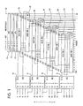
- Fig. 1 is a schematic diagram showing the invention as being embodied in a 16 by 16 bit multiplier array;
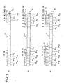
- Fig. 2 is a schematic diagram illustrating the special product generators for three times, five times, and seven times multiples of the multiplicand;
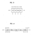
- Fig. 3 is a schematic diagram of a four bit carry look ahead adder;
- Fig. 4 is a schematic diagram illustrating a row of adders formed by combining five four-bit carry look ahead adders of Fig. 3;
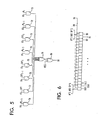
- Fig. 5 is a schematic logic diagram illustrating one bit of a selector circuit;
- Fig. 6 is a schematic diagram showing a selector circuit which is 20 bits wide where the logic for each bit is as shown in Fig. 5;
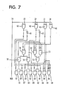
- Fig. 7 is a schematic logic diagram of the recode logic for the recode logic blocks shown in Fig. 1;
- Fig. 8 is a schematic diagram illustrating a formation of special products by shifting the multiplicand and performing an arithmetic operation;
- Fig. 9 is a schematic diagram illustrating multiples of the multiplicand;
- Fig. 10 is a schematic block diagram illustrating the recoding scheme; and,
- Fig. 11 is a schematic diagram of an alternate embodiment of the invention where the output is the sum of the product and a value Y.
- With reference to the drawings and particularly to Fig. 1, the invention is illustrated by way of example where the multiplicand is simultaneously applied to
special products generators recoders special products generators special products generator 15 is shown in detail in Fig. 2 and functions to generate an output which is three times the multiplicand. The low order bit position ofspecial products generator 15 has a forced zero signal applied toinput terminal 21 and a forced zero is applied to carry ininput terminal 22. The low order bit position of the multiplicand is applied tobit positions special products generator 15. Similarly, the other bits of the multiplicand are applied to the corresponding bit positions and the next higher bit position of thespecial products generator 15. Additionally,bit 15 of the multiplicand is applied to both inputs ofbit positions special products generator 15, the output fromspecial products generator 15 is three times the multiplicand. Thespecial products generator 15 functions to add the multiplicand to the multiplicand which has been shifted once. Of course, no shifting takes place dynamically because the multiplicand is applied to thespecial products generator 15 in shifted form. Thespecial products generator 15 has a 20-bit output, and thus it is necessary to connect the high order bit position of the multiplicand in the manner described in order to extend the sign bit of the multiplicand. The outputs of thespecial products generator 15 are applied as inputs intoselectors - The
special products generator 16 functions to generate a multiple which is five times the multiplicand. Thus, a forced zero is applied toterminal 23 as input into the low order and the next to the low order bit positions of thespecial products generator 16. A forced zero is applied to carry ininput terminal 24 connected to the low order bit position of thespecial products generator 16. The low order bit of the multiplicand is applied to the low order bit position and to the bit position two positions away from the low order bit position. The other bits of the multiplicand are applied to thespecial products generator 16 in a similar manner, and the high order bit position is applied tobit positions special products generator 16. Thespecial products generator 16 in essence adds the multiplicand to the multiplicand shifted twice. The multiplicand is applied to thespecial products generator 16 in the shifted form, and as previously indicated, no shifting takes place dynamically. The outputs of thespecial products generator 16 are applied to theselectors - The
special products generator 17 functions to form a multiple which is seven times the multiplicand. The multiplicand is applied as input into thespecial products generator 17 along with the multiplicand in shifted form three places to the left. However, in this instance the multiplicand is subtracted rather than added to the shifted form of the multiplicand because the shift provides a multiple which is eight times the multiplicand. The subtraction is accomplished by inverting the multiplicand throughinverters 27 and a forced 1 is applied to the carry ininput terminal 26. A forced 0 is applied toterminal 25 which is connected to the first three low order positions of thespecial products generator 17. The bits of the multiplicand are applied to the corresponding bit positions of thespecial products generator 17 viainverters 27 and in a noninverted form to bit positions three positions to the left of the corresponding bit input position. The high order bit of the multiplicand is applied throughinverters 27 tobit positions - The outputs of the
special products generator 17 are applied to theselectors selectors selector 70 is connected torecoder 30,selector 90 is connected torecoder 31,selector 100 is connected torecoder 32 andselector 110 is connected torecoder 33. Each selector has 20 bit positions, and each bit position includes a group ofAND circuits 71 to 78 shown in Fig. 5, whereAND circuit 71 has an X1 control or selector input from the associated recoder and an input from the multiplicand. Logical ANDcircuit 72 has an X2 input from the associated recoder and a bit, one bit position to the right of the multiplicand bit input toAND circuit 71. Logical ANDcircuit 73 has a X3 control input from the associated recoder and a bit from thespecial products generator 15. Logical ANDcircuit 74 has a X4 input from the associated recoder and a bit, two places to the right of the multiplicand input into logical ANDcircuit 71. Logical ANDcircuit 75 has a X5 input from the associated recoder and a bit fromspecial products generator 16. Logical AND circuit 36 has a X6 input from the associated recoder and a bit one position to the right of the bit from thespecial products generator 15 which is applied to logical ANDcircuit 73. Logical ANDcircuit 77 has an X7 input from the associated recoder and a bit from thespecial products generator 17. The logical ANDcircuit 78 has a X8 input from the associated recoder and a multiplicand input which is three places to the right of the multiplicand input into logical ANDcircuit 71. - The outputs of the logical AND circuits 71-78 are applied as inputs to logical OR
circuit 79 which has its output connected to an input of Exclusive ORcircuit 80. The other input into Exclusive ORcircuit 80 is the negative or NEG line from the associated recoder. The output ofExclusive OR circuit 80 is an output of the selector and it is connected as an input to an associated adder. A selector representative of theselectors - The rows of
adders - The
recoders recoder 31. Similarly, multiplier bits R7 and R11 are applied to inputs I0 ofrecoders recoders circuits circuits Exclusive OR circuits Exclusive OR circuits inverters circuit 50 has inputs from Exclusive ORcircuits circuit 51 has inputs fromExclusive OR circuit 40,Exclusive OR circuit 41, andinverter 47. NORcircuit 52 has inputs fromExclusive OR circuit 40,Exclusive OR circuit 41, andinverter 47. The outputs of ANDcircuit 51 and NORcircuit 52 feed ORcircuit 53. Exclusive ORcircuit 50 feeds ANDcircuits Exclusive OR circuit 42 andinverter 47 respectively. The X1, X2, X3, X4, X5, X6, X7, and X8 signals are from logical AND circuits 61-67 and NORcircuit 68, respectively. Exclusive ORcircuit 43 feeds ANDcircuits Inverter 48 feeds ANDcircuits circuit 55 feeds ANDcircuits circuit 54 feeds ANDcircuits circuit 53 feeds ANDcircuits circuits circuit 64 and to NORcircuit 68. NORcircuit 68 also has an input frominverter 48. The I4 input is the negative or NEG output of the recoder. - As seen in Fig.1, the outputs of the
recoders selectors recoders adders recoders selectors adders high order 16 bits ofadder 85 are inputs intoadder 95, thehigh order 16 bits ofadder 95 are inputs intoadder 105, and thehigh order 16 bits ofadder 105 are inputs intoadder 115. Thelow order 4 bits ofadders adder 115. - From the foregoing it is seen that multiples of the multiplicand are formed simultaneously and are applied as inputs into selectors together with the multiplicand itself where the selectors are controlled by recoders which have inputs from the multiplier. The selectors have their outputs connected to inputs of adders which form partial products where a low order adder has its outputs connected to inputs of the next higher order adder which also receives inputs from an associated selector. The highest order adder provides the high order bits of the product and each of the lower order adders provides lower order product bits, the number of bits being equal to the offset of the lower order adders i.e. in this example 4 bits.
- It should be noted that
adder 85 is not fully utilized as an adder and in fact is connected as an incrementor. The invention can be embodied so as to be a multiplier with a summing adder as shown in Fig. 11. In this embodiment,selector 70 feedsadders adder 85 is a 32-bit adder and its output is the sum of the product and an addend Y. Note that in this embodiment all of the adders are functioning as adders and none only as an incrementor. - While the preferred embodiment of the invention has been illustrated and described, it is to be understood that the invention is not to be limited to the precise construction herein disclosed and the right is reserved to all changes and modification coming within the scope of the invention as defined in the appended claims.
Claims (10)
a plurality of special products generators (15, 16, 17) having inputs for receiving predetermined bits of the multiplicand to generate therefrom outputs which are multiples of said multiplicand together with sign bits for said multiples of said multiplicand,
a plurality of recoders (30, 31, 32, 33) for recoding at least more than two bits of said multiplier to generate selection signals for selecting different multiples of the multiplicand including the multiplicand itself,
a plurality of selectors (70, 90, 100, 110) each connected to receive multiples of the multiplicand including the multiplicand itself and connected to receive said selection signals from said recoders; and,
a plurality of adders (85, 95, 105, 115) connected to said selectors and the outputs of said adders being interconnected to generate the product.
Applications Claiming Priority (2)
| Application Number | Priority Date | Filing Date | Title |
|---|---|---|---|
| US06/867,167 US4745570A (en) | 1986-05-27 | 1986-05-27 | Binary multibit multiplier |
| US867167 | 1986-05-27 |
Publications (2)
| Publication Number | Publication Date |
|---|---|
| EP0248166A2 true EP0248166A2 (en) | 1987-12-09 |
| EP0248166A3 EP0248166A3 (en) | 1990-09-05 |
Family
ID=25349259
Family Applications (1)
| Application Number | Title | Priority Date | Filing Date |
|---|---|---|---|
| EP19870104934 Withdrawn EP0248166A3 (en) | 1986-05-27 | 1987-04-03 | Binary multibit multiplier |
Country Status (3)
| Country | Link |
|---|---|
| US (1) | US4745570A (en) |
| EP (1) | EP0248166A3 (en) |
| JP (1) | JPS62280930A (en) |
Families Citing this family (18)
| Publication number | Priority date | Publication date | Assignee | Title |
|---|---|---|---|---|
| US4864528A (en) * | 1986-07-18 | 1989-09-05 | Matsushita Electric Industrial Co., Ltd. | Arithmetic processor and multiplier using redundant signed digit arithmetic |
| US4862402A (en) * | 1986-07-24 | 1989-08-29 | North American Philips Corporation | Fast multiplierless architecture for general purpose VLSI FIR digital filters with minimized hardware |
| US4864529A (en) * | 1986-10-09 | 1989-09-05 | North American Philips Corporation | Fast multiplier architecture |
| US4843585A (en) * | 1987-09-14 | 1989-06-27 | Motorola, Inc. | Pipelineable structure for efficient multiplication and accumulation operations |
| JP2991299B2 (en) * | 1989-08-04 | 1999-12-20 | 株式会社東芝 | Endoscope device |
| US4965762A (en) * | 1989-09-15 | 1990-10-23 | Motorola Inc. | Mixed size radix recoded multiplier |
| JPH0540608A (en) * | 1990-03-16 | 1993-02-19 | Internatl Business Mach Corp <Ibm> | Table look-up multiplier and multiplying method thereof |
| KR940002479B1 (en) * | 1990-03-20 | 1994-03-24 | 후지쓰 가부시끼가이샤 | High speed parallel multiplier |
| US5150322A (en) * | 1990-06-05 | 1992-09-22 | Vlsi Technology, Inc. | Mixed-radix serial/parallel multipliers |
| JP2597736B2 (en) * | 1990-07-17 | 1997-04-09 | 株式会社東芝 | Fast multiplier |
| US5412591A (en) * | 1990-08-09 | 1995-05-02 | Vlsi Technology, Inc. | Schematic compiler for a multi-format high speed multiplier |
| US5119325A (en) * | 1990-12-04 | 1992-06-02 | Motorola, Inc. | Multiplier having a reduced number of partial product calculations |
| US5361220A (en) * | 1991-11-29 | 1994-11-01 | Fuji Photo Film Co., Ltd. | Discrete cosine transformation with reduced components |
| JPH05204609A (en) * | 1992-01-13 | 1993-08-13 | Nec Corp | Multiplier |
| US5333119A (en) * | 1992-09-30 | 1994-07-26 | Regents Of The University Of Minnesota | Digital signal processor with delayed-evaluation array multipliers and low-power memory addressing |
| US5787029A (en) * | 1994-12-19 | 1998-07-28 | Crystal Semiconductor Corp. | Ultra low power multiplier |
| US5646877A (en) * | 1995-05-25 | 1997-07-08 | Texas Instruments Incorporated | High radix multiplier architecture |
| US6141674A (en) * | 1998-06-10 | 2000-10-31 | Hewlett-Packard Company | Reducing the hardware cost of a bank of multipliers by combining shared terms |
Citations (2)
| Publication number | Priority date | Publication date | Assignee | Title |
|---|---|---|---|---|
| US3372269A (en) * | 1961-06-30 | 1968-03-05 | Ibm | Multiplier for simultaneously generating partial products of various bits of the multiplier |
| EP0152046A2 (en) * | 1984-02-02 | 1985-08-21 | Nec Corporation | Multiplying circuit |
Family Cites Families (4)
| Publication number | Priority date | Publication date | Assignee | Title |
|---|---|---|---|---|
| US4041292A (en) * | 1975-12-22 | 1977-08-09 | Honeywell Information Systems Inc. | High speed binary multiplication system employing a plurality of multiple generator circuits |
| US4153938A (en) * | 1977-08-18 | 1979-05-08 | Monolithic Memories Inc. | High speed combinatorial digital multiplier |
| US4484301A (en) * | 1981-03-10 | 1984-11-20 | Sperry Corporation | Array multiplier operating in one's complement format |
| US4646257A (en) * | 1983-10-03 | 1987-02-24 | Texas Instruments Incorporated | Digital multiplication circuit for use in a microprocessor |
-
1986
- 1986-05-27 US US06/867,167 patent/US4745570A/en not_active Expired - Fee Related
-
1987
- 1987-04-03 EP EP19870104934 patent/EP0248166A3/en not_active Withdrawn
- 1987-04-15 JP JP62091068A patent/JPS62280930A/en active Pending
Patent Citations (2)
| Publication number | Priority date | Publication date | Assignee | Title |
|---|---|---|---|---|
| US3372269A (en) * | 1961-06-30 | 1968-03-05 | Ibm | Multiplier for simultaneously generating partial products of various bits of the multiplier |
| EP0152046A2 (en) * | 1984-02-02 | 1985-08-21 | Nec Corporation | Multiplying circuit |
Non-Patent Citations (2)
| Title |
|---|
| ELECTRONICS LETTERS, vol. 16, no. 2, January 1980, pages 53-54, Herts, GB; E. AMBIKAIRAJAH et al.: "Technique for performing multiplication on a 16-bit microprocessor using an extension of Booth's algorithm" * |
| IBM TECHNICAL DISCLOSURE BULLETIN, vol. 27, no. 11, April 1985, pages 6624-6632, New York, US; "Improved approach to the use of Booth's multiplication algorithm" * |
Also Published As
| Publication number | Publication date |
|---|---|
| US4745570A (en) | 1988-05-17 |
| EP0248166A3 (en) | 1990-09-05 |
| JPS62280930A (en) | 1987-12-05 |
Similar Documents
| Publication | Publication Date | Title |
|---|---|---|
| US4745570A (en) | Binary multibit multiplier | |
| EP0239899B1 (en) | Multiplier array circuit | |
| US3100835A (en) | Selecting adder | |
| US4813008A (en) | Multiplier circuit suitable for obtaining a negative product of a multiplier and a multiplicand | |
| US4130878A (en) | Expandable 4 × 8 array multiplier | |
| EP0152046A2 (en) | Multiplying circuit | |
| US4965762A (en) | Mixed size radix recoded multiplier | |
| US6704762B1 (en) | Multiplier and arithmetic unit for calculating sum of product | |
| GB2399909A (en) | Multiplication of selectively partitioned binary inputs using booth encoding | |
| EP0137386B1 (en) | Digital multiplying circuit | |
| US4215419A (en) | Method for binary multiplication of a number by a sum of two numbers and a digital system for implementation thereof | |
| JPS5856033A (en) | Multiplying circuit | |
| US5677863A (en) | Method of performing operand increment in a booth recoded multiply array | |
| US5787031A (en) | Divider and multiplier/divider using said divider | |
| US5521855A (en) | Multiplying circuit | |
| US5691930A (en) | Booth encoder in a binary multiplier | |
| US6167422A (en) | Booth multiplication structure which selectively integrates the function of either of incrementing or negating with the function of booth multiplication | |
| JPH05173761A (en) | Binary integer multiplier | |
| US5119325A (en) | Multiplier having a reduced number of partial product calculations | |
| EP0545654B1 (en) | Digital multiplier circuit | |
| GB2226165A (en) | Parallel carry generation adder | |
| EP0326414A2 (en) | High speed multiplier | |
| JP2606339B2 (en) | Multiplier | |
| JP2734438B2 (en) | Multiplier | |
| KR0146255B1 (en) | Modified booth multiplier |
Legal Events
| Date | Code | Title | Description |
|---|---|---|---|
| PUAI | Public reference made under article 153(3) epc to a published international application that has entered the european phase |
Free format text: ORIGINAL CODE: 0009012 |
|
| AK | Designated contracting states |
Kind code of ref document: A2 Designated state(s): DE FR GB |
|
| 17P | Request for examination filed |
Effective date: 19880329 |
|
| PUAL | Search report despatched |
Free format text: ORIGINAL CODE: 0009013 |
|
| AK | Designated contracting states |
Kind code of ref document: A3 Designated state(s): DE FR GB |
|
| 17Q | First examination report despatched |
Effective date: 19920302 |
|
| STAA | Information on the status of an ep patent application or granted ep patent |
Free format text: STATUS: THE APPLICATION IS DEEMED TO BE WITHDRAWN |
|
| 18D | Application deemed to be withdrawn |
Effective date: 19920915 |
|
| RIN1 | Information on inventor provided before grant (corrected) |
Inventor name: DIEDRICH, RICHARD ALAN Inventor name: LAWRENCE, JAY ALLEN |