EP0247722A1 - Homodyne Verbindungen von integrierten Schaltungen - Google Patents
Homodyne Verbindungen von integrierten Schaltungen Download PDFInfo
- Publication number
- EP0247722A1 EP0247722A1 EP87303491A EP87303491A EP0247722A1 EP 0247722 A1 EP0247722 A1 EP 0247722A1 EP 87303491 A EP87303491 A EP 87303491A EP 87303491 A EP87303491 A EP 87303491A EP 0247722 A1 EP0247722 A1 EP 0247722A1
- Authority
- EP
- European Patent Office
- Prior art keywords
- optical interconnection
- circuit
- optical
- interconnection system
- modulator
- Prior art date
- Legal status (The legal status is an assumption and is not a legal conclusion. Google has not performed a legal analysis and makes no representation as to the accuracy of the status listed.)
- Granted
Links
Images
Classifications
-
- H—ELECTRICITY
- H04—ELECTRIC COMMUNICATION TECHNIQUE
- H04B—TRANSMISSION
- H04B10/00—Transmission systems employing electromagnetic waves other than radio-waves, e.g. infrared, visible or ultraviolet light, or employing corpuscular radiation, e.g. quantum communication
- H04B10/60—Receivers
- H04B10/61—Coherent receivers
-
- G—PHYSICS
- G02—OPTICS
- G02B—OPTICAL ELEMENTS, SYSTEMS OR APPARATUS
- G02B6/00—Light guides; Structural details of arrangements comprising light guides and other optical elements, e.g. couplings
- G02B6/10—Light guides; Structural details of arrangements comprising light guides and other optical elements, e.g. couplings of the optical waveguide type
- G02B6/12—Light guides; Structural details of arrangements comprising light guides and other optical elements, e.g. couplings of the optical waveguide type of the integrated circuit kind
- G02B6/12004—Combinations of two or more optical elements
-
- H—ELECTRICITY
- H04—ELECTRIC COMMUNICATION TECHNIQUE
- H04B—TRANSMISSION
- H04B10/00—Transmission systems employing electromagnetic waves other than radio-waves, e.g. infrared, visible or ultraviolet light, or employing corpuscular radiation, e.g. quantum communication
- H04B10/60—Receivers
- H04B10/61—Coherent receivers
- H04B10/63—Homodyne, i.e. coherent receivers where the local oscillator is locked in frequency and phase to the carrier signal
Definitions
- This invention relates to interconnection of electrical elements by optical means, and in particular to interconnection of elements on semiconductor wafers and interconnections between separate wafers.
- wafers includes both comparatively small dimensioned chips and also larger slices.
- Optical interconnection has been proposed as a way of reducing delays and adverse electrical interactions, with direct detection of the incoming optical signal by photo detectors. (J.W. Goodman et al. "Optical Interconnection for VLSI Systems” Proc. IEEE, Vol. 72, No. 7, July 1984).
- a disadvantage of proposed systems is that direct detection necessitates low noise, multi-stage amplification and therefore at the detection end of the optical link fabrication complexity is greatly increased, although it is possible to fabricate all the elements from silicon.
- At the transmission end in order to modulate an optical signal in accordance with an output signal from a silicon integrated circuit with sufficient strength to enable direct detection it has been considered necessary to incorporate separate modulators or to fabricate modulators or light sources from Group III-V materials, again adding greatly to fabrication complexity.
- the present invention provides an optical interconnection for integrated circuits employing homodyne detection, comprising a coherent light source the output of which provides both the carrier signal for modulation with the information to be transmitted, and the local oscillator signal required for homodyne detection.
- the present invention provides an optical interconnection system for integrated circuits comprising an optical source supplying a carrier wave comprising at least two parts and a modulator at which a first part of the wave is modulated in accordance with an output signal from a first circuit, a second part of the wave passing unmodulated to a second circuit where it is mixed with the modulated carrier in homodyne detection to provide an input signal to the second circuit.
- the modulation and detection takes place respectively on the same wafer as the first and second circuits and are fabricated integrally of the same material.
- the wafer or wafers are preferably made of silicon and the optical transmission frequency is on or close to the band edge absorption frequency.
- optical' source includes electro-optical sources.
- Optical is to be construed as including the visible spectrum and also the infra-red and ultra-violet parts of the electro-magnetic spectrum.
- Homodyne detection of modulated optical signals is generally acknowledged to be the most sensitive technique of detection and yields high gain even from weak modulation.
- homodyne detection requires the detector to be provided with a signal (termed the local oscillator signal) of the same frequency and phase as the incoming carrier; it is also generally the most difficult detection technique to implement, especially when the carrier frequency may be subject to drift.
- the carrier beam is split prior to modulation and the unmodulated beam is utilised as the local oscillator input.
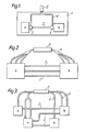
- a silicon chip 1 has a first circuit area A that requires connection to a second circuit area B.
- the connection between areas A and B is made by a waveguide or optical fibre 2 that connects a modulator 3 associated with area A to a detector 4 associated with area B.
- An external narrow optical line width laser 5 provides an unmodulated input optical signal to the modulator 3 where the optical signal is modulated by the electrical signal output from circuit area A.
- the modulated signal is transmitted along waveguide 2 to detector 4 where it is mixed with light of the same phase and frequency for homodyne detection.
- the local oscillator input to the detector 4 is provided by supplying light directly from laser 5, along local oscillator path 6 by splitting the output from laser 5 upstream of the modulator.
- the light from the local oscillator path 6 is automatically in the required phase and of the same frequency. Any tendency for frequency drift in the laser, and hence in the carrier frequency, is immediately compensated by a similar change in the unmodulated carrier wave input as the local oscillator wave.
- the sensitivity of homodyne detection enables both silicon based modulators and detectors to be used in order to simplify the fabrication process for an all silicon integrated circuit. However, for some applications it is envisaged that other materials will be deposited on to the silicon to form the modulator.
- Optical detectors operating at wavelengths up to the region of about 1100 nm can readily be fabricated in silicon and a silicon optical modulator operating close to or on that wavelength (that is, close to or on the absorption band edge) would be usable because the signal, although weak, would be readily detectable by the homodyne method.
- the amplification requirements after homodyne detection are less stringent than required in direct detection and a single narrow band amplifier can be used, again simplifying fabrication.
- the optical link may comprise optical fibres either free or attached to the wafer, or for a waveguide to be fabricated within the wafer itself, for example an etched channel filled with suitably doped silicon dioxide or other optically transmissive medium (as Phys. Vol. 19 No. 7, July 1980, ppL372-L374).
- the optical communication may be through free space (or atmosphere), but in this instance alignment and scattering can create problems.
- the links from laser to wafer and between wafers to be via optical fibres and the links within a wafer to be via on-wafer routes.
- FIG 2 illustrates a second embodiment of the invention in which a plurality of interconnections between circuits A and B utilise the same source laser.
- Each circuit A has a modulator associated with each input carrier wave and each circuit B has a detector associated with each unmodulated local oscillator input.
- the circuits A and B may be on a single wafer or they may be on separate wafers.
- the output beam from each end of laser 5 is used, the two output beams being identical.
- Each of the beams could be used for either A or B circuits or for combinations.
- Figure 3 illustrates a further progression with more circuits from which it will be realised that a single source laser may power a complete system of circuits.
- the interconnection may be made in free space or, preferably, in waveguides such as optical fibres.
- gas lasers may be employed as each modulator detector pair will preferably operate on a wave of 10 to 100 microwatts power.
- optical interconnections may be utilised as part of an integrated optical or optoelectronic device in addition to providing the function of conducting the signal between parts of an electronic system. It is envisaged that a given detector may receive signals from a plurality of modulators. The electrical signals from several circuits may be combined and transmitted along a single optical link, the sensitivity of homodyne detection enabling easier separation than direct detection.
- the delay caused by optical transmission of signals depends upon the speed of light in the optical medium concerned.
- silica light propagates at about 2 x 10⁸ m/sec and therefore a 1 cm track introduces a delay of only 50 psec.
- the optical interconnections are less than 1 metre in length.
- circuits comprising electronic, optical or optoelectronic elements.
Landscapes
- Physics & Mathematics (AREA)
- Engineering & Computer Science (AREA)
- Electromagnetism (AREA)
- Computer Networks & Wireless Communication (AREA)
- Signal Processing (AREA)
- General Physics & Mathematics (AREA)
- Microelectronics & Electronic Packaging (AREA)
- Optics & Photonics (AREA)
- Semiconductor Lasers (AREA)
- Optical Communication System (AREA)
- Production Of Multi-Layered Print Wiring Board (AREA)
- Optical Integrated Circuits (AREA)
- Use Of Switch Circuits For Exchanges And Methods Of Control Of Multiplex Exchanges (AREA)
Priority Applications (1)
| Application Number | Priority Date | Filing Date | Title |
|---|---|---|---|
| AT87303491T ATE67909T1 (de) | 1986-05-19 | 1987-04-21 | Homodyne verbindungen von integrierten schaltungen. |
Applications Claiming Priority (2)
| Application Number | Priority Date | Filing Date | Title |
|---|---|---|---|
| GB868612072A GB8612072D0 (en) | 1986-05-19 | 1986-05-19 | Homodyne interconnections of integrated circuits |
| GB8612072 | 1986-05-19 |
Publications (2)
| Publication Number | Publication Date |
|---|---|
| EP0247722A1 true EP0247722A1 (de) | 1987-12-02 |
| EP0247722B1 EP0247722B1 (de) | 1991-09-25 |
Family
ID=10598049
Family Applications (1)
| Application Number | Title | Priority Date | Filing Date |
|---|---|---|---|
| EP87303491A Expired - Lifetime EP0247722B1 (de) | 1986-05-19 | 1987-04-21 | Homodyne Verbindungen von integrierten Schaltungen |
Country Status (9)
| Country | Link |
|---|---|
| US (1) | US4844571A (de) |
| EP (1) | EP0247722B1 (de) |
| JP (1) | JPH0626248B2 (de) |
| AT (1) | ATE67909T1 (de) |
| CA (1) | CA1280170C (de) |
| DE (1) | DE3773262D1 (de) |
| ES (1) | ES2025652T3 (de) |
| GB (1) | GB8612072D0 (de) |
| GR (1) | GR3002801T3 (de) |
Cited By (2)
| Publication number | Priority date | Publication date | Assignee | Title |
|---|---|---|---|---|
| WO2002099481A3 (en) * | 2001-06-01 | 2003-09-18 | Motorola Inc | Semiconductor structure for an optically switched integrated device |
| EP0899900A3 (de) * | 1997-08-28 | 2004-10-06 | Alcatel | Verfahren zur optischen Übertragung über ein Lichtwellenleiternetz, sowie optisches Übertragungsnetz |
Families Citing this family (20)
| Publication number | Priority date | Publication date | Assignee | Title |
|---|---|---|---|---|
| GB9105435D0 (en) * | 1991-03-14 | 1991-05-01 | Bicc Plc | Optical cable joints |
| US6392257B1 (en) | 2000-02-10 | 2002-05-21 | Motorola Inc. | Semiconductor structure, semiconductor device, communicating device, integrated circuit, and process for fabricating the same |
| AU2001257346A1 (en) | 2000-05-31 | 2001-12-11 | Motorola, Inc. | Semiconductor device and method for manufacturing the same |
| WO2002009187A2 (en) | 2000-07-24 | 2002-01-31 | Motorola, Inc. | Heterojunction tunneling diodes and process for fabricating same |
| US20020096683A1 (en) | 2001-01-19 | 2002-07-25 | Motorola, Inc. | Structure and method for fabricating GaN devices utilizing the formation of a compliant substrate |
| WO2002082551A1 (en) | 2001-04-02 | 2002-10-17 | Motorola, Inc. | A semiconductor structure exhibiting reduced leakage current |
| US6992321B2 (en) | 2001-07-13 | 2006-01-31 | Motorola, Inc. | Structure and method for fabricating semiconductor structures and devices utilizing piezoelectric materials |
| US7019332B2 (en) | 2001-07-20 | 2006-03-28 | Freescale Semiconductor, Inc. | Fabrication of a wavelength locker within a semiconductor structure |
| US6855992B2 (en) | 2001-07-24 | 2005-02-15 | Motorola Inc. | Structure and method for fabricating configurable transistor devices utilizing the formation of a compliant substrate for materials used to form the same |
| US20030034491A1 (en) | 2001-08-14 | 2003-02-20 | Motorola, Inc. | Structure and method for fabricating semiconductor structures and devices for detecting an object |
| US20030071327A1 (en) | 2001-10-17 | 2003-04-17 | Motorola, Inc. | Method and apparatus utilizing monocrystalline insulator |
| US6916717B2 (en) | 2002-05-03 | 2005-07-12 | Motorola, Inc. | Method for growing a monocrystalline oxide layer and for fabricating a semiconductor device on a monocrystalline substrate |
| US7169619B2 (en) | 2002-11-19 | 2007-01-30 | Freescale Semiconductor, Inc. | Method for fabricating semiconductor structures on vicinal substrates using a low temperature, low pressure, alkaline earth metal-rich process |
| US6885065B2 (en) | 2002-11-20 | 2005-04-26 | Freescale Semiconductor, Inc. | Ferromagnetic semiconductor structure and method for forming the same |
| US6965128B2 (en) | 2003-02-03 | 2005-11-15 | Freescale Semiconductor, Inc. | Structure and method for fabricating semiconductor microresonator devices |
| US7020374B2 (en) | 2003-02-03 | 2006-03-28 | Freescale Semiconductor, Inc. | Optical waveguide structure and method for fabricating the same |
| US7489836B2 (en) * | 2003-03-17 | 2009-02-10 | Intel Corporation | Optical interconnect system for high speed microprocessor input/output (IO) |
| US7366368B2 (en) * | 2004-06-15 | 2008-04-29 | Intel Corporation | Optical add/drop interconnect bus for multiprocessor architecture |
| US20070122156A1 (en) * | 2005-11-28 | 2007-05-31 | Tongqing Wang | Apparatus, system, and method for interconnecting electrical and electronic signals |
| WO2015162671A1 (ja) * | 2014-04-21 | 2015-10-29 | 富士通株式会社 | 波長可変レーザ光源、光送信器及び光送受信器モジュール |
Citations (3)
| Publication number | Priority date | Publication date | Assignee | Title |
|---|---|---|---|---|
| EP0016608A1 (de) * | 1979-03-15 | 1980-10-01 | University Of Delaware | Verfahren und Vorrichtung zur Signalübertragung über eine optische Faser |
| EP0150929A2 (de) * | 1984-01-16 | 1985-08-07 | Texas Instruments Incorporated | Substrat mit optischen Verbindungssystemen zwischen den auf dem Substrat montierten Bausteinen |
| EP0168192A2 (de) * | 1984-07-02 | 1986-01-15 | AT&T Corp. | Empfänger für ein Lichtwellenübertragungssystem mit Homodynempfang |
Family Cites Families (1)
| Publication number | Priority date | Publication date | Assignee | Title |
|---|---|---|---|---|
| JPS5915423B2 (ja) * | 1981-07-15 | 1984-04-09 | 日本電信電話株式会社 | マザ−ボ−ド及びパツケ−ジ間光接続方式 |
-
1986
- 1986-05-19 GB GB868612072A patent/GB8612072D0/en active Pending
-
1987
- 1987-04-21 DE DE8787303491T patent/DE3773262D1/de not_active Expired - Lifetime
- 1987-04-21 EP EP87303491A patent/EP0247722B1/de not_active Expired - Lifetime
- 1987-04-21 ES ES198787303491T patent/ES2025652T3/es not_active Expired - Lifetime
- 1987-04-21 AT AT87303491T patent/ATE67909T1/de not_active IP Right Cessation
- 1987-04-23 CA CA000535362A patent/CA1280170C/en not_active Expired - Lifetime
- 1987-05-18 US US07/050,572 patent/US4844571A/en not_active Expired - Fee Related
- 1987-05-19 JP JP62123607A patent/JPH0626248B2/ja not_active Expired - Lifetime
-
1991
- 1991-09-26 GR GR91401375T patent/GR3002801T3/el unknown
Patent Citations (3)
| Publication number | Priority date | Publication date | Assignee | Title |
|---|---|---|---|---|
| EP0016608A1 (de) * | 1979-03-15 | 1980-10-01 | University Of Delaware | Verfahren und Vorrichtung zur Signalübertragung über eine optische Faser |
| EP0150929A2 (de) * | 1984-01-16 | 1985-08-07 | Texas Instruments Incorporated | Substrat mit optischen Verbindungssystemen zwischen den auf dem Substrat montierten Bausteinen |
| EP0168192A2 (de) * | 1984-07-02 | 1986-01-15 | AT&T Corp. | Empfänger für ein Lichtwellenübertragungssystem mit Homodynempfang |
Non-Patent Citations (2)
| Title |
|---|
| ELECTRONIC DESIGN, vol. 30, no. 11, May 1982, pages 44-45, Waseca, MN, Denville, NJ, US; M. GROSSMAN: "Optical devices in wells join electronic circuitry on a chip" * |
| PATENT ABSTRACTS OF JAPAN, vol. 7, no. 84 (E-169)[1229], 8th April 1983; & JP-A-58 12 451 (NIPPON DENSHIN DENWA KOSHA) 24-01-1983 * |
Cited By (2)
| Publication number | Priority date | Publication date | Assignee | Title |
|---|---|---|---|---|
| EP0899900A3 (de) * | 1997-08-28 | 2004-10-06 | Alcatel | Verfahren zur optischen Übertragung über ein Lichtwellenleiternetz, sowie optisches Übertragungsnetz |
| WO2002099481A3 (en) * | 2001-06-01 | 2003-09-18 | Motorola Inc | Semiconductor structure for an optically switched integrated device |
Also Published As
| Publication number | Publication date |
|---|---|
| JPS62285466A (ja) | 1987-12-11 |
| ES2025652T3 (es) | 1992-04-01 |
| GR3002801T3 (en) | 1993-01-25 |
| EP0247722B1 (de) | 1991-09-25 |
| GB8612072D0 (en) | 1986-06-25 |
| ATE67909T1 (de) | 1991-10-15 |
| JPH0626248B2 (ja) | 1994-04-06 |
| CA1280170C (en) | 1991-02-12 |
| US4844571A (en) | 1989-07-04 |
| DE3773262D1 (de) | 1991-10-31 |
Similar Documents
| Publication | Publication Date | Title |
|---|---|---|
| EP0247722B1 (de) | Homodyne Verbindungen von integrierten Schaltungen | |
| US11437786B2 (en) | Polarization insensitive colorless optical devices | |
| US10338308B2 (en) | Method and system for partial integration of wavelength division multiplexing and bi-directional solutions | |
| US11143816B2 (en) | Method and system for stabilized directional couplers | |
| US4671605A (en) | Length dependent, optical time delay/filter device for electrical signals | |
| JPS6135586A (ja) | レーザダイオード、入力伝送フアイバおよび出力伝送フアイバを有する電気光学装置 | |
| EP0351133A2 (de) | Optisches polarisationsunempfindliches Übertragungsgerät mit optischer Vorverstärkung | |
| JPS62114340A (ja) | 双方向光通信装置 | |
| JPS62116030A (ja) | コヒ−レントな光波のトランスミツタ | |
| US5721637A (en) | Wavelength converter apparatus | |
| US6282015B1 (en) | Wavelength converter | |
| US7064891B2 (en) | Optical wavelength converter with a semiconductor optical amplifier | |
| CN118842527A (zh) | 基于多材料平台的集成微波光子处理芯片 | |
| US6904100B1 (en) | Pulse controlled phase modulator | |
| Qian et al. | Hybrid polymer THz receiver PIC with waveguide integrated photoconductive antenna: Concept and 1st characterization results | |
| US6587256B2 (en) | RF combiner based on cascaded optical phase modulation | |
| JP4014020B2 (ja) | 光信号処理システム | |
| JP2002006357A (ja) | 光信号を加算および減算するための電気光学的装置 | |
| Shaw et al. | Optoelectronic integrated circuits for microwave optical systems | |
| GB2110498A (en) | Laser telecommunications system | |
| Seeds | Microwave opto-electronics: principles, applications and future prospects | |
| Sobol | Overview of the Application of Microwave Techniques for Lightwave Systems-Invited | |
| Chen et al. | High-speed board-to-board optical interconnection | |
| Novotny et al. | Two dimensional optical data links | |
| BLANK et al. | High-capacity lightwave transmission systems |
Legal Events
| Date | Code | Title | Description |
|---|---|---|---|
| PUAI | Public reference made under article 153(3) epc to a published international application that has entered the european phase |
Free format text: ORIGINAL CODE: 0009012 |
|
| AK | Designated contracting states |
Kind code of ref document: A1 Designated state(s): AT BE CH DE ES FR GB GR IT LI LU NL SE |
|
| 17P | Request for examination filed |
Effective date: 19880506 |
|
| 17Q | First examination report despatched |
Effective date: 19900706 |
|
| GRAA | (expected) grant |
Free format text: ORIGINAL CODE: 0009210 |
|
| AK | Designated contracting states |
Kind code of ref document: B1 Designated state(s): AT BE CH DE ES FR GB GR IT LI LU NL SE |
|
| REF | Corresponds to: |
Ref document number: 67909 Country of ref document: AT Date of ref document: 19911015 Kind code of ref document: T |
|
| ITF | It: translation for a ep patent filed | ||
| REF | Corresponds to: |
Ref document number: 3773262 Country of ref document: DE Date of ref document: 19911031 |
|
| ET | Fr: translation filed | ||
| REG | Reference to a national code |
Ref country code: ES Ref legal event code: FG2A Ref document number: 2025652 Country of ref document: ES Kind code of ref document: T3 |
|
| PLBE | No opposition filed within time limit |
Free format text: ORIGINAL CODE: 0009261 |
|
| STAA | Information on the status of an ep patent application or granted ep patent |
Free format text: STATUS: NO OPPOSITION FILED WITHIN TIME LIMIT |
|
| 26N | No opposition filed | ||
| REG | Reference to a national code |
Ref country code: GR Ref legal event code: FG4A Free format text: 3002801 |
|
| PGFP | Annual fee paid to national office [announced via postgrant information from national office to epo] |
Ref country code: FR Payment date: 19940309 Year of fee payment: 8 |
|
| PGFP | Annual fee paid to national office [announced via postgrant information from national office to epo] |
Ref country code: SE Payment date: 19940315 Year of fee payment: 8 Ref country code: AT Payment date: 19940315 Year of fee payment: 8 |
|
| PGFP | Annual fee paid to national office [announced via postgrant information from national office to epo] |
Ref country code: GB Payment date: 19940316 Year of fee payment: 8 |
|
| PGFP | Annual fee paid to national office [announced via postgrant information from national office to epo] |
Ref country code: GR Payment date: 19940324 Year of fee payment: 8 Ref country code: BE Payment date: 19940324 Year of fee payment: 8 |
|
| PGFP | Annual fee paid to national office [announced via postgrant information from national office to epo] |
Ref country code: CH Payment date: 19940325 Year of fee payment: 8 |
|
| PGFP | Annual fee paid to national office [announced via postgrant information from national office to epo] |
Ref country code: LU Payment date: 19940331 Year of fee payment: 8 |
|
| PGFP | Annual fee paid to national office [announced via postgrant information from national office to epo] |
Ref country code: ES Payment date: 19940406 Year of fee payment: 8 Ref country code: DE Payment date: 19940406 Year of fee payment: 8 |
|
| PGFP | Annual fee paid to national office [announced via postgrant information from national office to epo] |
Ref country code: NL Payment date: 19940430 Year of fee payment: 8 |
|
| EPTA | Lu: last paid annual fee | ||
| EAL | Se: european patent in force in sweden |
Ref document number: 87303491.2 |
|
| PG25 | Lapsed in a contracting state [announced via postgrant information from national office to epo] |
Ref country code: LU Free format text: LAPSE BECAUSE OF NON-PAYMENT OF DUE FEES Effective date: 19950421 Ref country code: GB Effective date: 19950421 Ref country code: AT Effective date: 19950421 |
|
| PG25 | Lapsed in a contracting state [announced via postgrant information from national office to epo] |
Ref country code: SE Effective date: 19950422 Ref country code: ES Free format text: LAPSE BECAUSE OF NON-PAYMENT OF DUE FEES Effective date: 19950422 |
|
| PG25 | Lapsed in a contracting state [announced via postgrant information from national office to epo] |
Ref country code: LI Effective date: 19950430 Ref country code: CH Effective date: 19950430 Ref country code: BE Effective date: 19950430 |
|
| BERE | Be: lapsed |
Owner name: BRITISH TELECOMMUNICATIONS P.L.C. Effective date: 19950430 |
|
| PG25 | Lapsed in a contracting state [announced via postgrant information from national office to epo] |
Ref country code: GR Free format text: THE PATENT HAS BEEN ANNULLED BY A DECISION OF A NATIONAL AUTHORITY Effective date: 19951031 |
|
| PG25 | Lapsed in a contracting state [announced via postgrant information from national office to epo] |
Ref country code: NL Effective date: 19951101 |
|
| REG | Reference to a national code |
Ref country code: CH Ref legal event code: PL |
|
| GBPC | Gb: european patent ceased through non-payment of renewal fee |
Effective date: 19950421 |
|
| PG25 | Lapsed in a contracting state [announced via postgrant information from national office to epo] |
Ref country code: FR Effective date: 19951229 |
|
| REG | Reference to a national code |
Ref country code: GR Ref legal event code: MM2A Free format text: 3002801 |
|
| NLV4 | Nl: lapsed or anulled due to non-payment of the annual fee |
Effective date: 19951101 |
|
| PG25 | Lapsed in a contracting state [announced via postgrant information from national office to epo] |
Ref country code: DE Effective date: 19960103 |
|
| EUG | Se: european patent has lapsed |
Ref document number: 87303491.2 |
|
| REG | Reference to a national code |
Ref country code: FR Ref legal event code: ST |
|
| REG | Reference to a national code |
Ref country code: ES Ref legal event code: FD2A Effective date: 19990201 |
|
| PG25 | Lapsed in a contracting state [announced via postgrant information from national office to epo] |
Ref country code: IT Free format text: LAPSE BECAUSE OF NON-PAYMENT OF DUE FEES;WARNING: LAPSES OF ITALIAN PATENTS WITH EFFECTIVE DATE BEFORE 2007 MAY HAVE OCCURRED AT ANY TIME BEFORE 2007. THE CORRECT EFFECTIVE DATE MAY BE DIFFERENT FROM THE ONE RECORDED. Effective date: 20050421 |