EP0246750B1 - Disposition de connexion électrique pour la distribution de différents niveaux de puissance à un circuit imprimé - Google Patents
Disposition de connexion électrique pour la distribution de différents niveaux de puissance à un circuit imprimé Download PDFInfo
- Publication number
- EP0246750B1 EP0246750B1 EP87303470A EP87303470A EP0246750B1 EP 0246750 B1 EP0246750 B1 EP 0246750B1 EP 87303470 A EP87303470 A EP 87303470A EP 87303470 A EP87303470 A EP 87303470A EP 0246750 B1 EP0246750 B1 EP 0246750B1
- Authority
- EP
- European Patent Office
- Prior art keywords
- projection
- connector
- terminal
- mating
- board
- Prior art date
- Legal status (The legal status is an assumption and is not a legal conclusion. Google has not performed a legal analysis and makes no representation as to the accuracy of the status listed.)
- Expired - Lifetime
Links
- 230000013011 mating Effects 0.000 claims description 34
- 239000002131 composite material Substances 0.000 claims description 13
- 239000004033 plastic Substances 0.000 claims description 7
- 229920003023 plastic Polymers 0.000 claims description 7
- 239000000463 material Substances 0.000 claims description 5
- 230000000295 complement effect Effects 0.000 claims description 4
- 238000000926 separation method Methods 0.000 claims description 3
- 230000003247 decreasing effect Effects 0.000 claims description 2
- 239000002184 metal Substances 0.000 claims 1
- 210000000887 face Anatomy 0.000 description 11
- 238000004519 manufacturing process Methods 0.000 description 3
- 230000009977 dual effect Effects 0.000 description 2
- 230000015572 biosynthetic process Effects 0.000 description 1
- 238000001816 cooling Methods 0.000 description 1
- 230000000694 effects Effects 0.000 description 1
- 238000004100 electronic packaging Methods 0.000 description 1
- 239000000835 fiber Substances 0.000 description 1
- 238000003780 insertion Methods 0.000 description 1
- 230000037431 insertion Effects 0.000 description 1
- 238000009413 insulation Methods 0.000 description 1
- 238000000465 moulding Methods 0.000 description 1
- 210000001331 nose Anatomy 0.000 description 1
- 230000008707 rearrangement Effects 0.000 description 1
- 230000000717 retained effect Effects 0.000 description 1
- 238000005096 rolling process Methods 0.000 description 1
Images


Classifications
-
- H—ELECTRICITY
- H01—ELECTRIC ELEMENTS
- H01R—ELECTRICALLY-CONDUCTIVE CONNECTIONS; STRUCTURAL ASSOCIATIONS OF A PLURALITY OF MUTUALLY-INSULATED ELECTRICAL CONNECTING ELEMENTS; COUPLING DEVICES; CURRENT COLLECTORS
- H01R13/00—Details of coupling devices of the kinds covered by groups H01R12/70 or H01R24/00 - H01R33/00
- H01R13/46—Bases; Cases
- H01R13/514—Bases; Cases composed as a modular blocks or assembly, i.e. composed of co-operating parts provided with contact members or holding contact members between them
-
- H—ELECTRICITY
- H01—ELECTRIC ELEMENTS
- H01R—ELECTRICALLY-CONDUCTIVE CONNECTIONS; STRUCTURAL ASSOCIATIONS OF A PLURALITY OF MUTUALLY-INSULATED ELECTRICAL CONNECTING ELEMENTS; COUPLING DEVICES; CURRENT COLLECTORS
- H01R12/00—Structural associations of a plurality of mutually-insulated electrical connecting elements, specially adapted for printed circuits, e.g. printed circuit boards [PCB], flat or ribbon cables, or like generally planar structures, e.g. terminal strips, terminal blocks; Coupling devices specially adapted for printed circuits, flat or ribbon cables, or like generally planar structures; Terminals specially adapted for contact with, or insertion into, printed circuits, flat or ribbon cables, or like generally planar structures
- H01R12/70—Coupling devices
- H01R12/7005—Guiding, mounting, polarizing or locking means; Extractors
- H01R12/7011—Locking or fixing a connector to a PCB
-
- H—ELECTRICITY
- H01—ELECTRIC ELEMENTS
- H01R—ELECTRICALLY-CONDUCTIVE CONNECTIONS; STRUCTURAL ASSOCIATIONS OF A PLURALITY OF MUTUALLY-INSULATED ELECTRICAL CONNECTING ELEMENTS; COUPLING DEVICES; CURRENT COLLECTORS
- H01R12/00—Structural associations of a plurality of mutually-insulated electrical connecting elements, specially adapted for printed circuits, e.g. printed circuit boards [PCB], flat or ribbon cables, or like generally planar structures, e.g. terminal strips, terminal blocks; Coupling devices specially adapted for printed circuits, flat or ribbon cables, or like generally planar structures; Terminals specially adapted for contact with, or insertion into, printed circuits, flat or ribbon cables, or like generally planar structures
- H01R12/70—Coupling devices
- H01R12/7088—Arrangements for power supply
-
- H—ELECTRICITY
- H01—ELECTRIC ELEMENTS
- H01R—ELECTRICALLY-CONDUCTIVE CONNECTIONS; STRUCTURAL ASSOCIATIONS OF A PLURALITY OF MUTUALLY-INSULATED ELECTRICAL CONNECTING ELEMENTS; COUPLING DEVICES; CURRENT COLLECTORS
- H01R12/00—Structural associations of a plurality of mutually-insulated electrical connecting elements, specially adapted for printed circuits, e.g. printed circuit boards [PCB], flat or ribbon cables, or like generally planar structures, e.g. terminal strips, terminal blocks; Coupling devices specially adapted for printed circuits, flat or ribbon cables, or like generally planar structures; Terminals specially adapted for contact with, or insertion into, printed circuits, flat or ribbon cables, or like generally planar structures
- H01R12/70—Coupling devices
- H01R12/71—Coupling devices for rigid printing circuits or like structures
- H01R12/72—Coupling devices for rigid printing circuits or like structures coupling with the edge of the rigid printed circuits or like structures
- H01R12/73—Coupling devices for rigid printing circuits or like structures coupling with the edge of the rigid printed circuits or like structures connecting to other rigid printed circuits or like structures
- H01R12/735—Printed circuits including an angle between each other
- H01R12/737—Printed circuits being substantially perpendicular to each other
-
- G—PHYSICS
- G02—OPTICS
- G02B—OPTICAL ELEMENTS, SYSTEMS OR APPARATUS
- G02B6/00—Light guides; Structural details of arrangements comprising light guides and other optical elements, e.g. couplings
- G02B6/24—Coupling light guides
- G02B6/36—Mechanical coupling means
- G02B6/38—Mechanical coupling means having fibre to fibre mating means
- G02B6/3807—Dismountable connectors, i.e. comprising plugs
- G02B6/3873—Connectors using guide surfaces for aligning ferrule ends, e.g. tubes, sleeves, V-grooves, rods, pins, balls
- G02B6/3874—Connectors using guide surfaces for aligning ferrule ends, e.g. tubes, sleeves, V-grooves, rods, pins, balls using tubes, sleeves to align ferrules
- G02B6/3878—Connectors using guide surfaces for aligning ferrule ends, e.g. tubes, sleeves, V-grooves, rods, pins, balls using tubes, sleeves to align ferrules comprising a plurality of ferrules, branching and break-out means
- G02B6/3879—Linking of individual connector plugs to an overconnector, e.g. using clamps, clips, common housings comprising several individual connector plugs
-
- G—PHYSICS
- G02—OPTICS
- G02B—OPTICAL ELEMENTS, SYSTEMS OR APPARATUS
- G02B6/00—Light guides; Structural details of arrangements comprising light guides and other optical elements, e.g. couplings
- G02B6/24—Coupling light guides
- G02B6/36—Mechanical coupling means
- G02B6/38—Mechanical coupling means having fibre to fibre mating means
- G02B6/3807—Dismountable connectors, i.e. comprising plugs
- G02B6/3897—Connectors fixed to housings, casing, frames or circuit boards
-
- H—ELECTRICITY
- H01—ELECTRIC ELEMENTS
- H01R—ELECTRICALLY-CONDUCTIVE CONNECTIONS; STRUCTURAL ASSOCIATIONS OF A PLURALITY OF MUTUALLY-INSULATED ELECTRICAL CONNECTING ELEMENTS; COUPLING DEVICES; CURRENT COLLECTORS
- H01R13/00—Details of coupling devices of the kinds covered by groups H01R12/70 or H01R24/00 - H01R33/00
- H01R13/64—Means for preventing incorrect coupling
- H01R13/645—Means for preventing incorrect coupling by exchangeable elements on case or base
Definitions
- the invention relates to an electrical connector arrangement for the distribution of different levels of power to a printed circuit board.
- FR-A-2 493 051 discloses a connector arrangement for the distribution of different levels of power between printed circuit boards comprising first and second pairs of matable individual connectors having different power carrying characteristics, a first connector of each pair having a pluggable mating face located transversely of a board-engaging face and the second connector of each pair having a complementary pluggable mating face located opposite a board-engaging face so that the first connectors of each pair can be mounted in a row along one edge of a daughter board with the mating faces extending perpendicular to the plane of the board and the second individual connector of respective pairs can be mounted in a row along the face of a mother board with matable connectors of respective pairs located in corresponding positions and their mating faces extending parallel to the plane of the mother board whereby the daughter board can be releasably connected to the mother board for simultaneous distribution of different power levels thereto by mating of the connectors in a simple plugging action.
- a disadvantage of the connector arrangement described in the above-mentioned document is that the relative positions of the different connector types are arranged only by fixing the connectors to the circuit boards, and dedication of the circuit boards to only a single connector arrangement to meet only a single power supply requirement is necessary at the time of manufacture of the boards.
- the alignment and assembly of the connectors on the boards can be relatively difficult and time-consuming.
- the connectors are modular, the first individual modules of respective pairs being provided with means to link them together with other mutually opposite faces of the first modules adjacent to form a first composite connector body, and the second individual connectors of respective first and second pairs being provided with means to link them together with other mutually opposite faces of the modules adjacent to form a second composite connector body, the relative positions of the first and second individual modules in the composite bodies being interchangeable.
- the composite bodies are programmable prior to application to the circuit boards to meet alternative mixed power requirements. Furthermore, they are readily adapted for automated assembly together to form the different composite connector bodies enabling the manufacturer to standardize circuit board layout.
- the board engaging faces of the modules have the same common dimensions, facilitating further standardisation of the circuit board manufacture to meet different combinations of power level requirement.
- a programmable modular connector assembly is described in EP-A-0 152 743, but the modules must be retained in juxtaposition by a separate frame or carrier and do not enable a daughter board to be plugged directly to a mother board to obtain the necessary supply of different power levels. Either frames of different sizes to accommodate different numbers of modules for different power supply requirements must be supplied, or a single frame oversize for many needs increasing the cost and unnecessary use of circuit board space. In addition, extra steps are required to complete the assembly of the modular connector to the printed circuit board.
- a problem that is met in supplying higher current to printed circuit boards using terminals of small size is the formation of hot spots caused by uneven current flow through various locations in the terminal and at points of connection to the circuit board, with consequential risk of damage to the connectors' connections (particularly when soldered) and the circuit board.
- Such a terminal may have terminal posts which extend from the terminal at different locations for connection to the circuit board and are of different resistivities, thereby to tend to equalise the current flow and avoid hot spots caused by high current concentrations.
- a further problem that may be met is providing a compact polarising structure which can be readily changed to obtain different settings with simple tools.
- DE-A-1 938 791 discloses a set of terminal blocks which can be mechanically interlocked with each other by means of hooked portions of the blocks.
- the blocks do not, however, receive electrical terminals which can be mated by mating pluggable mating faces of the blocks, but have bores in which wires can be secured by means of set screws in the blocks.
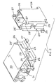
- the modular connector assembly comprises first, second, and third pairs of matable individual connector modules 11,11 ⁇ ; 12,12 ⁇ ; and 13,13 ⁇ , respectively, each pair having contacts with different current-carrying characteristics.
- Each first connector module 11,12 or 13 of each pair has a board connecting face 17 located transversely of a pluggable mating face 18 and each second connector module 11 ⁇ ,12 ⁇ or 13 ⁇ of each pair has a board-connecting portion 19 located opposite a pluggable mating face 21.
- the board-connecting portions have the same common dimensions.
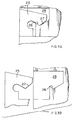
- Each module is provided on respective other, mutually opposite, faces 24,24 ⁇ with latch means to link them together comprising a plurality of interengageable hooks and catches 25 and 26 which face in opposite rotational senses on respective faces 24 and 24 ⁇ .
- Each face is rectangular and the hooks and catches 25 and 26 are located on alternate corners equidistant from a central rotational axis at which is located a pivot pin on one face 24 and a socket on the other face 24 ⁇ .
- the hooks 25 are resilient and are formed with camming noses 27 such that they can flex to engage the catches 26 which are located in pockets 28 formed in the face during movement from the condition of Figure 3A to that of Figure 3B.
- Each face is formed with recesses 29,29 ⁇ opening at corresponding locations, which recesses are brought into registration to form cooling cavities 31 when the modules are rotated together to bring the hooks and catches into latching engagement.
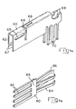
- first connector modules of different current-carrying types can be latched together to form a composite connector half mounted by means of end modules 30 having similar latching means and coding pins 31, projecting from mating faces without the need for further support, and such composite connector half mounted to extend along one edge of a daughter board 33 for plugging engagement with a similar composite connector half comprising individual second connector modules mounted (with complementary end modules 30 ⁇ ) on the face of a mother board to form a modular connector assembly to distribute various different power inputs between the mother and daughter boards.
- the composite connector half formed by the second individual connectors can be mounted in a bulkhead rather than on the mother board.
- An advantage of the particular latching means is that the rotational movement needed for latching together individual modules precludes inadvertent unlatching.
- modules may be adapted to carry fibre optic power supplies to the boards.
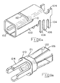
- Terminal 60 includes a forwardly extending, inverted, channel-section body portion 62 which is relatively long and narrow and is formed with adjacent, longitudinally and transversely extending, stiffening embossments 65 and 64, respectively, defining a front mouth.
- a locking barb 66 extends outwardly rearwardly from the base of the channel and engages a projection or shoulder in the housing interior to secure the terminal 60 therewithin. The rear end is cut away to define catches 69 which project rearwardly and upwardly from the side walls to anchor an insulating cap, described below.
- a row of three pairs of aligned posts 70 which are soldered or force fit in apertures in the daughter board connecting to pad 71 extend from the channel side walls adjacent the rear.
- Rearwardly spaced successive posts are of decreasing effective length with respect to their connection points to the daughter board to balance out the current flow through the terminals and posts, total resistance of the forward posts being larger than the rearward posts, so that current flowing through the terminal 60 from the mouth will be more evenly distributed through each post, thereby distributing the heat generated by current flow more evenly through the terminal posts and circuitry of the board.
- Equalising the current flow by varying the length of the posts enables the posts to be of standard cross-sectional size, obviating any requirement for the provision of nonstandard conductive pads or paths on the circuit boards which would add to the cost.
- this enables the posts to be located in equally spaced-apart relation, providing both a stable mounting for the terminal and an evenly distributed current flow in the circuit board.
- the terminal may be made of dual thickness stock, the rear portion from which the posts extend being of thicker stock than the forward portion better to carry the high currents concentrated therein.
- the embossment 64 may be omitted.
- stamped and formed male terminal 80 includes multiple posts 82 for connection to pad 81 and a like number of cantilever spring contact fingers 84 substantially evenly spaced from respective posts, extending rearwardly and forwardly from respective opposite edges of a planar body portion 85, providing conductive paths of equal length and resistance from the mother board 34 ⁇ to the mouth 67 of the mating terminal 60.
- Alternate contact fingers 84 diverge from a planar body portion 85 in opposite senses and their free ends 86 are curved back towards each other facilitating mating with terminal 60 without stubbing and providing multiple evenly-spaced points of contact on the opposite sides of the terminal 60 for optimum current distribution.
- the male terminal is very inexpensive to manufacture yet provides an effective current carrying connection to paths 81 on the mother board 34 ⁇ .
- the terminals are recessed from the forward mating faces of the module housings to avoid shorting.
- the housing 61 is open at a rear end and integrally formed by moulding with a tubular mating portion 88 and a channel section rearward portion 89 with the channel mouth open to the circuit board.
- a plastic cap 90 is formed with fingers 92 by which it can be snap fitted into the rear of module 61 by the fingers engaging the projections 69 and the rearmost of the legs 70 of terminal 60. The cap 90 assures insulation of the terminals 60 while permitting the housing to be moulded in a simple straight-draw mould.
- the contact combination of terminals 60 and 80 has a design rating in excess of fifteen amperes at 280 volts D.C. so that each module 12 has a design rating of thirty amperes or better. It should be noted that this relatively high current rating is achieved in a very narrow box-like configuration which minimises occupation of board space, such boards being very costly particularly with heavy gauge, high current, capacity.
- Terminal 100 is similar to the previously described terminal and includes a tubular body 100 with a forward, mating receptacle portion of rectangular cross section, with a bevelled mouth 102 formed with longitudinal and transverse embossments 112 and 110, board connecting post pairs 104,106,108, and catches 104.
- the male terminal 120 is stamped and formed from dual thickness stock and includes a series of cantilever spring contact fingers 122,124 extending generally coaxially forwardly and rearwardly, respectively, from aligned locations equally spaced around the periphery of a tubular body portion 121.
- the contact fingers 122 diverge radially outwardly as they extend towards their free ends which are bent inwardly to avoid stubbing on mating.
- the housing of module 11 ⁇ is integrally moulded with centrally located, forwardly extending, tapering tubular projection 130, having a free end of further reduced diameter extending beyond the free ends of the terminal, the body portion and contact fingers of which are received in a recess defined between the projection 130 and an outer wall 136 of the module.
- the divergence maintains a separation between the projection 130 and contact portions of the contact finger adjacent the free ends, and avoids a rolling action on engagement with the housing of module 11.
- the plastics housing modules 234,236, respectively are generally similar in overall shape to those 30,30 ⁇ shown schematically and are formed with respective hexagonal section cavities 238,240 receiving a polarising projection (not in Figure 1 version) and key 242,244, respectively, and intersected by bowed snap ring receiving slots 246,248, respectively.
- Access recesses 250,252 are formed with guiding abutment surfaces 254,256 for receipt of a lever release tool, such as the blade of a screwdriver receivable in an eye 247 provided in a tab 249 of the ring.
- Each snap ring 258 is formed with three radially inwardly protruding groove engaging lands 259,260,261 at a free end of each leg and at a central location, respectively.
- the end walls of the mating modules are provided with a resilient cantilever latching arm 264 having a latching eye 266 receiving a latching ramp 268 in known manner.
- the polarising projection 242 is moulded of plastic material with a hexagonal section body with a snap ring receiving groove 270 at a rear end and an eccentrically located, axially longitudinally extending key receiving slot 272.
- the cavity 240 of module 232 has a hexagonal section counterbore 274 at a rear end of smaller cross-sectional size than a front projection receiving portion 275 receiving a hexagonal section rear body portion 276 of the key 244 which is locked in position in a similar manner to projection 242.
- a forward mating portion 278 of the key is of semihexagonal section and projects through the front cavity portion 275 at an eccentric location. Both the mating portion 278 of the key and a forward portion of the projection protrude from the mating face beyond mating ends of the other modules and internest when mated, as shown in Figure 8B, beyond the opposed faces, avoiding a need for an excessively long projection for effective guiding which would arise if a projection from only one module were provided.
- the modular concept permits intermating of several different kinds of modules in a way which fixes dimensions and allows a preassembly of modules prior to insertion in printed circuit boards, occupies relatively little board space, and provides several types of power terminals having themselves features to better assure distribution of current without hot spots, and a particular type of polarisation which allows considerable flexibility in adapting to electrical and electronic packaging.
Claims (11)
- Assemblage de connecteurs pour la distribution de différents niveaux de puissance entre des cartes (33, 34') à circuits inprimés, comportant des première et seconde paires de connecteurs individuels accouplables (11, 11' ; 12, 12' ; 13, 13') ayant des caractéristiques de transport de puissance différentes, un premier connecteur (11, 12, 13) de chaque paire (11, 11' ; 12, 12' ; 13, 13') ayant une face d'accouplement enfichable (18) disposée transversalement à une face (17) d'engagement de carte et le second connecteur (11', 12', 13') de chaque paire (11, 11' ; 12, 12' ; 13, 13') ayant une face d'accouplement enfichable complémentaire (21) située de façon à être opposée à une face (19) d'engagement de carte afin que les premiers connecteurs (11, 12, 13) de chaque paire (11, 11' ; 12, 12' ; 13, 13') puissent être montés en une rangée le long d'un bord d'une carte-fille (33), les faces d'accouplement (18) s'étendant perpendiculairement au plan de le carte (33), et que les seconds connecteurs individuels (11', 12', 13') des paires respectives (11, 11' ; 12, 12' ; 13, 13') puissent être montés en une rangée le long de la face d'une carte-mère (34), des connecteurs accouplables (11, 11' ; 12, 12' ; 13, 13') de paires respectives étant placés dans des positions correspondantes et leurs faces d'accouplement (21) s'étendant parallèlement au plan de la carte-mère (34') de manière que la carte-fille (33) puisse être connectée de façon amovible à la carte-mère (34') pour une distribution simultanée à celle-ci de différents niveaux de puissance par l'accouplement des connecteurs (11, 11' ; 12, 12' ; 13, 13') en une action d'enfichage simple,
caractérisé en ce que les connecteurs (11, 11' ; 12, 12' ; 13, 13') sont modulaires, des premiers modules individuels (11, 12, 13) de paires respectives étant pourvus de moyens (25, 26) destinés à les relier entre eux, d'autres faces mutuellement opposées (24, 24') des premiers modules (11, 12, 13) étant adjacentes, pour former un premier corps de connecteur composé, et les seconds connecteurs individuels (11', 12', 13') des première et seconde paires respectives (11, 11' ; 12, 12' ; 13, 13') étant pourvues de moyens (25, 26) destinés à les relier entre eux, d'autres faces mutuellement opposées (24, 24') des modules (11', 12', 13') étant adjacentes, pour former un second corps de connecteur composé, les positions relatives des premiers et seconds modules individuels (11, 11' ; 12, 12' ; 13, 13') dans les corps composés étant interchangeables. - Assemblage de connecteurs selon la revendication 1, caractérisé en ce que les faces (17, 19) d'engagement de cartes des modules (11, 11' ; 12, 12' ; 13, 13') ont les mêmes dimensions communes.
- Assemblage de connecteurs selon la revendication 1 ou la renvendication 2, caractérisé en ce que les moyens de liaison (25, 26) des modules individuels (11, 11' ; 12, 12' ; 13, 13') de paires respectives sont hermaphrodites.
- Assemblage de connecteurs selon l'une quelconque des revendications précédentes, caractérisé en ce qu'une première des paires de modules (11, 11' ou 12, 12') de connecteurs est destinée à porter des niveaux de courant élevés, le premier module (11 ou 12) de connecteurs de la première paire (11, 11' ou 12, 12') comprenant une borne (60 ou 100) ayant une partie avant de contact (67 ou 102) à une face de contact (18), une partie de corps (62 ou 100) s'étendent longitudinalement vers l'arrière depuis la partie de contact (67, 102), et une série de broches (70 ou 104, 106, 108) de connexion à une carte à circuit s'étendant depuis la partie de corps (62 ou 100) à des intervilles espacés longitudinalement, les broches successives (70 ou 108, 106, 104), qui sont séparées d'une distance croissante de la partie de contact (67 ou 102), étant de résistivités différentes afin de tendre à égaliser le flux de courant passant par ces broches (70 ou 108, 106, 104) vers le circuit de la carte-fille.
- Assemblage de connecteurs selon la revendication 4, caractérisé en ce que des broches successives (70 ou 108, 106, 104) sont de longueurs utiles décroissantes afin que leurs résistivités respectives diminuent.
- Assemblage de connecteurs selon la revendications 5, caractérisé en ce que la borne (60 ou 100) est découpée et formée en métal en feuilles et la partie de contact (67 ou 102) définit une douille ayant des parois latérales opposées reliées par une parois de base, les broches (70 ou 108, 106, 104) s'étendant en deux rangées depuis les parties arrière des parois latérales respectives.
- Asssemblage de connecteurs selon la revendication 6, caractérisé en ce que la borne (60 ou 100) est accrochée dans un boîtier (61) moulé en matière plastique avec une partie tubulaire avant (88) le long de laquelle la douille (62) s'étend axialement et une partie arrière (89) de section en gouttière s'ouvrant vers la carte (33) à circuit, ouverture à travers laquelle les broches (70 ou 108, 106, 104) s'étendent, des moyens d'accrochage (69, 104) étant formés par des parties arrière des parois latérales de la borne, en un emplacement espacé des broches (70 ou 108, 106, 104) de la borne, un chapeau (90, 140) moulé en matière plastique comportant des doigts élastiques (92) de verrouillage qui en font saillie et qui peuvent s'enclencher avec les moyens d'accrochage (69, 104) pour verrouiller le chapeau (90, 140) sur l'extrémité arrière du boîtier (61) afin de fermer l'extrémité arrière.
- Assemblage de connecteurs selon la revendication 1, caractérisé par une borne (60 ou 100) destinée à conduire un courant intense entre des première et seconde interfaces de contact comprenant une partie de contact (67 ou 102) destinée à recevoir un courant d'une première interface de contact, une partie de corps (62 ou 100) s'étendant longitudinalement à l'écart de la partie de contact (67 ou 102), et une série de broches (70 ou 108, 106, 104) de connexion de cartes à circuits s'étendant depuis la partie de corps (62 ou 100) à des intervalles espacés longitudinalement, dans lequel des broches successives (70 ou 108, 106, 104), qui sont séparées d'une distance croissante de la partie de contact (67 ou 102), étant de résistivités différentes afin de tendre à égaliser le flux de courant passant par ces broches (70 ou 108, 106, 104) vers une seconde interface de contact.
- Assemblage de connecteurs selon la revendication 1, caractérisé par un module (11') de connecteurs transportant un courant intense, ayant un boîtier moulé d'une seule pièce en matière plastique et comprenant une paroi extérieure (136) définissant un logement ayant une partie avant ouverte et une saillie (130) située centralement à l'intérieur du logement et s'étendant vers la partie avant de manière que soit défini, entre la paroi (136) et la saillie (130), un premier évidement de réception de borne ; une borne (120) reçue dans l'évidement et ayant un anneau de doigts (122) de contact à ressort en porte-à-faux faisant saillie vers l'avant autour de la saillie (130) en un emplacement établi en arrière d'une extrémité avant de la saillie (130), afin qu'une borne d'accouplement de forme complémentaire de celle de la borne (120) puisse être reçue dans le logement en enclenchement électrique d'accouplement avec elle, la saillie empêchant un contact manuel accidentel avec la borne (120) dans un état désaccouplé du module (11') de connecteurs.
- Assemblage de connecteurs selon la revendication 1, caractérisé par une paire (30, 30' ou 230, 232) de modules de polarisation dont un module (230) comprend un boitier (234) moulé en matière plastique et présentant une cavité (238) à faces multiples, une saillie (242) de polarisation ayant une surface correspondante à faces multiples destinée à être reçue dans ladite cavité (234) dans des positions différentes, en rotation, correspondant à l'opposition de faces différentes respectives de la cavité (234) et de la saillie (242), une extrémité avant de la saillie (242) étant exempte d'une face d'accouplement du boîtier pour réaliser un engagement d'accouplement avec une cavité correspondante (240) à faces multiples de l'autre module (232) de la paire (230, 232), l'autre extrémité de la saillie (242) étant formée de façon à présenter une gorge (270) et un anneau à encliqueter destiné à être inséré à travers une ouverture d'accès (250) dans le boîtier (234) pour amener des doigts opposés respectifs de l'anneau à encliqueter dans la gorge (270) afin de verrouiller la saillie axialement dans le boîtier (234) dans l'une quelconque des positions en rotation, une partie extrême (249) de l'anneau à encliqueter s'étendant depuis le boîtier pour être engagée par un outil de libération afin de retirer l'anneau à encliqueter de la gorge pour libérer ainsi la saillie (242) pour sa libération de la cavité (238) et une rotation vers une autre position de polarisation.
- Assemblage de connecteurs selon la revendication 10, caractérisé en ce que la saillie (242) est formée de façon à présenter une rainure (272) de réception d'une clavette située de façon à s'étendre axialement et excentriquement sur sa longueur, le boîtier (236) de l'autre module (232) étant pourvu d'une clavette (244) située de façon à faire saillie excentriquement de la cavité (240) de l'autre module (232) depuis la face d'accouplement dans l'une de plusieurs positions en rotation, afin que la clavette (244) soit reçue dans la rainure (272) lorsque la saillie (242) est accouplée avec la cavité (240) de l'autre module (230) pour réaliser un accouplement polarisé des paires (230, 232) de modules.
Applications Claiming Priority (6)
| Application Number | Priority Date | Filing Date | Title |
|---|---|---|---|
| US85522586A | 1986-04-22 | 1986-04-22 | |
| US855225 | 1986-04-22 | ||
| US07/907,703 US4790763A (en) | 1986-04-22 | 1986-09-15 | Programmable modular connector assembly |
| US907703 | 1986-09-15 | ||
| US07/907,696 US4820169A (en) | 1986-04-22 | 1986-09-15 | Programmable modular connector assembly |
| US907696 | 1986-09-15 |
Publications (3)
| Publication Number | Publication Date |
|---|---|
| EP0246750A2 EP0246750A2 (fr) | 1987-11-25 |
| EP0246750A3 EP0246750A3 (en) | 1988-01-27 |
| EP0246750B1 true EP0246750B1 (fr) | 1992-09-16 |
Family
ID=27420377
Family Applications (1)
| Application Number | Title | Priority Date | Filing Date |
|---|---|---|---|
| EP87303470A Expired - Lifetime EP0246750B1 (fr) | 1986-04-22 | 1987-04-21 | Disposition de connexion électrique pour la distribution de différents niveaux de puissance à un circuit imprimé |
Country Status (2)
| Country | Link |
|---|---|
| EP (1) | EP0246750B1 (fr) |
| DE (1) | DE3781715T2 (fr) |
Families Citing this family (10)
| Publication number | Priority date | Publication date | Assignee | Title |
|---|---|---|---|---|
| US4818237A (en) * | 1987-09-04 | 1989-04-04 | Amp Incorporated | Modular plug-in connection means for flexible power supply of electronic apparatus |
| DE29602740U1 (de) * | 1996-02-21 | 1996-04-11 | Phoenix Contact Gmbh & Co | Elektrischer Steckverbinder |
| US5915975A (en) * | 1996-09-12 | 1999-06-29 | Molex Incorporated | Surface mount connector with integrated power leads |
| US20020013090A1 (en) * | 1996-10-07 | 2002-01-31 | Donald L. Oros | Electrical connector for and i/o module |
| NO982678L (no) * | 1997-06-26 | 1998-12-28 | Siemens Ag | Pluggkoblingsstykke |
| GB9913347D0 (en) * | 1999-06-08 | 1999-08-11 | Albright International Ltd | A contactor |
| US7247058B2 (en) * | 2005-08-25 | 2007-07-24 | Tyco Electronics Corporation | Vertical docking connector |
| EP2423721B1 (fr) * | 2010-08-25 | 2015-11-11 | CCS Technology, Inc. | Adaptateur pour recevoir une pièce de connecteur hybride et pièce de connecteur à fibres optiques |
| CN103178396A (zh) * | 2011-12-21 | 2013-06-26 | 英业达股份有限公司 | 电子系统及其导引接合装置 |
| CN112277673A (zh) * | 2020-10-16 | 2021-01-29 | 国创新能源汽车智慧能源装备创新中心(江苏)有限公司 | 一种通道选择器及pdu系统 |
Family Cites Families (3)
| Publication number | Priority date | Publication date | Assignee | Title |
|---|---|---|---|---|
| FR2493051A1 (fr) * | 1980-10-23 | 1982-04-30 | Cit Alcatel | Connecteur d'energie pour cartes |
| US4519667A (en) * | 1982-05-06 | 1985-05-28 | Rockwell International Corporation | Electrical connector |
| EP0152743A1 (fr) * | 1984-01-27 | 1985-08-28 | Litton Precision Products International GmbH | Connecteur électrique modulaire |
-
1987
- 1987-04-21 DE DE8787303470T patent/DE3781715T2/de not_active Expired - Fee Related
- 1987-04-21 EP EP87303470A patent/EP0246750B1/fr not_active Expired - Lifetime
Also Published As
| Publication number | Publication date |
|---|---|
| EP0246750A2 (fr) | 1987-11-25 |
| EP0246750A3 (en) | 1988-01-27 |
| DE3781715D1 (de) | 1992-10-22 |
| DE3781715T2 (de) | 1993-04-29 |
Similar Documents
| Publication | Publication Date | Title |
|---|---|---|
| US4820169A (en) | Programmable modular connector assembly | |
| US4790763A (en) | Programmable modular connector assembly | |
| EP1393416B1 (fr) | Ensemble connecteur electrique a zones de production d'arc electrique separees | |
| US6004158A (en) | Electrical connector with secondary locking plates | |
| US4762500A (en) | Impedance matched electrical connector | |
| US4818237A (en) | Modular plug-in connection means for flexible power supply of electronic apparatus | |
| EP0829930B1 (fr) | Connecteur électrique avec contacts de puissance | |
| US8435047B2 (en) | Modular connectors with easy-connect capability | |
| US7591683B2 (en) | Contact terminal, extender with improved ground contact, and method for making the extender | |
| EP1393413B1 (fr) | Connecteur de connexion de carte et procede de production dudit connecteur | |
| US5882214A (en) | Electrical connector with contact assembly | |
| US6663427B1 (en) | High density electrical connector assembly | |
| US7824187B1 (en) | High density connector | |
| EP0390450A1 (fr) | Connecteur empilable dos à dos pour bus d'interface | |
| EP0717468B1 (fr) | Connecteur interrompant d'abord les contacts polaires et après le contact à la terre | |
| US7491083B2 (en) | Electrical connector assembly | |
| EP0246750B1 (fr) | Disposition de connexion électrique pour la distribution de différents niveaux de puissance à un circuit imprimé | |
| EP0152743A1 (fr) | Connecteur électrique modulaire | |
| US6350159B1 (en) | Arrangement for preventing mismating of connectors having different numbers of terminals | |
| JPH0799706B2 (ja) | モジュール型コネクタ | |
| US5194018A (en) | Electrical connector assembly and method of fabricating same | |
| US4175818A (en) | Electrical connectors | |
| JPH08293346A (ja) | 電気コネクタ及びコネクタ組立体 | |
| US6074230A (en) | Hermaphroditic electrical connectors | |
| US6821164B2 (en) | Connector assembly comprising a tab-receiving insulated spring sleeve and a dual contact with pairs of spaced apart contact members and tails |
Legal Events
| Date | Code | Title | Description |
|---|---|---|---|
| PUAI | Public reference made under article 153(3) epc to a published international application that has entered the european phase |
Free format text: ORIGINAL CODE: 0009012 |
|
| AK | Designated contracting states |
Kind code of ref document: A2 Designated state(s): DE FR GB IT |
|
| PUAL | Search report despatched |
Free format text: ORIGINAL CODE: 0009013 |
|
| AK | Designated contracting states |
Kind code of ref document: A3 Designated state(s): DE FR GB IT |
|
| 17P | Request for examination filed |
Effective date: 19880629 |
|
| RAP1 | Party data changed (applicant data changed or rights of an application transferred) |
Owner name: AMP INCORPORATED |
|
| 17Q | First examination report despatched |
Effective date: 19910221 |
|
| ITTA | It: last paid annual fee | ||
| GRAA | (expected) grant |
Free format text: ORIGINAL CODE: 0009210 |
|
| AK | Designated contracting states |
Kind code of ref document: B1 Designated state(s): DE FR GB IT |
|
| REF | Corresponds to: |
Ref document number: 3781715 Country of ref document: DE Date of ref document: 19921022 |
|
| ET | Fr: translation filed | ||
| ITF | It: translation for a ep patent filed |
Owner name: GUZZI E RAVIZZA S.R.L. |
|
| PLBE | No opposition filed within time limit |
Free format text: ORIGINAL CODE: 0009261 |
|
| STAA | Information on the status of an ep patent application or granted ep patent |
Free format text: STATUS: NO OPPOSITION FILED WITHIN TIME LIMIT |
|
| 26N | No opposition filed | ||
| REG | Reference to a national code |
Ref country code: GB Ref legal event code: 732E |
|
| PGFP | Annual fee paid to national office [announced via postgrant information from national office to epo] |
Ref country code: GB Payment date: 19960318 Year of fee payment: 10 |
|
| PGFP | Annual fee paid to national office [announced via postgrant information from national office to epo] |
Ref country code: FR Payment date: 19960412 Year of fee payment: 10 |
|
| PGFP | Annual fee paid to national office [announced via postgrant information from national office to epo] |
Ref country code: DE Payment date: 19960430 Year of fee payment: 10 |
|
| PG25 | Lapsed in a contracting state [announced via postgrant information from national office to epo] |
Ref country code: GB Effective date: 19970421 |
|
| GBPC | Gb: european patent ceased through non-payment of renewal fee |
Effective date: 19970421 |
|
| PG25 | Lapsed in a contracting state [announced via postgrant information from national office to epo] |
Ref country code: FR Free format text: LAPSE BECAUSE OF NON-PAYMENT OF DUE FEES Effective date: 19971231 |
|
| PG25 | Lapsed in a contracting state [announced via postgrant information from national office to epo] |
Ref country code: DE Free format text: LAPSE BECAUSE OF NON-PAYMENT OF DUE FEES Effective date: 19980101 |
|
| REG | Reference to a national code |
Ref country code: FR Ref legal event code: ST |
|
| PG25 | Lapsed in a contracting state [announced via postgrant information from national office to epo] |
Ref country code: IT Free format text: LAPSE BECAUSE OF NON-PAYMENT OF DUE FEES;WARNING: LAPSES OF ITALIAN PATENTS WITH EFFECTIVE DATE BEFORE 2007 MAY HAVE OCCURRED AT ANY TIME BEFORE 2007. THE CORRECT EFFECTIVE DATE MAY BE DIFFERENT FROM THE ONE RECORDED. Effective date: 20050421 |