EP0244925B1 - Programmable logic controller - Google Patents
Programmable logic controller Download PDFInfo
- Publication number
- EP0244925B1 EP0244925B1 EP87300869A EP87300869A EP0244925B1 EP 0244925 B1 EP0244925 B1 EP 0244925B1 EP 87300869 A EP87300869 A EP 87300869A EP 87300869 A EP87300869 A EP 87300869A EP 0244925 B1 EP0244925 B1 EP 0244925B1
- Authority
- EP
- European Patent Office
- Prior art keywords
- signals
- output
- signal
- counter
- programmable
- Prior art date
- Legal status (The legal status is an assumption and is not a legal conclusion. Google has not performed a legal analysis and makes no representation as to the accuracy of the status listed.)
- Expired - Lifetime
Links
Images

Classifications
-
- G—PHYSICS
- G05—CONTROLLING; REGULATING
- G05B—CONTROL OR REGULATING SYSTEMS IN GENERAL; FUNCTIONAL ELEMENTS OF SUCH SYSTEMS; MONITORING OR TESTING ARRANGEMENTS FOR SUCH SYSTEMS OR ELEMENTS
- G05B19/00—Program-control systems
- G05B19/02—Program-control systems electric
- G05B19/04—Program control other than numerical control, i.e. in sequence controllers or logic controllers
- G05B19/045—Program control other than numerical control, i.e. in sequence controllers or logic controllers using logic state machines, consisting only of a memory or a programmable logic device containing the logic for the controlled machine and in which the state of its outputs is dependent on the state of its inputs or part of its own output states, e.g. binary decision controllers, finite state controllers
-
- G—PHYSICS
- G06—COMPUTING OR CALCULATING; COUNTING
- G06F—ELECTRIC DIGITAL DATA PROCESSING
- G06F9/00—Arrangements for program control, e.g. control units
- G06F9/06—Arrangements for program control, e.g. control units using stored programs, i.e. using an internal store of processing equipment to receive or retain programs
- G06F9/30—Arrangements for executing machine instructions, e.g. instruction decode
- G06F9/30003—Arrangements for executing specific machine instructions
- G06F9/30007—Arrangements for executing specific machine instructions to perform operations on data operands
- G06F9/30036—Instructions to perform operations on packed data, e.g. vector, tile or matrix operations
- G06F9/30038—Instructions to perform operations on packed data, e.g. vector, tile or matrix operations using a mask
-
- G—PHYSICS
- G06—COMPUTING OR CALCULATING; COUNTING
- G06F—ELECTRIC DIGITAL DATA PROCESSING
- G06F9/00—Arrangements for program control, e.g. control units
- G06F9/06—Arrangements for program control, e.g. control units using stored programs, i.e. using an internal store of processing equipment to receive or retain programs
- G06F9/30—Arrangements for executing machine instructions, e.g. instruction decode
- G06F9/30003—Arrangements for executing specific machine instructions
- G06F9/3005—Arrangements for executing specific machine instructions to perform operations for flow control
- G06F9/30054—Unconditional branch instructions
-
- G—PHYSICS
- G06—COMPUTING OR CALCULATING; COUNTING
- G06F—ELECTRIC DIGITAL DATA PROCESSING
- G06F9/00—Arrangements for program control, e.g. control units
- G06F9/06—Arrangements for program control, e.g. control units using stored programs, i.e. using an internal store of processing equipment to receive or retain programs
- G06F9/30—Arrangements for executing machine instructions, e.g. instruction decode
- G06F9/30003—Arrangements for executing specific machine instructions
- G06F9/3005—Arrangements for executing specific machine instructions to perform operations for flow control
- G06F9/30061—Multi-way branch instructions, e.g. CASE
-
- G—PHYSICS
- G05—CONTROLLING; REGULATING
- G05B—CONTROL OR REGULATING SYSTEMS IN GENERAL; FUNCTIONAL ELEMENTS OF SUCH SYSTEMS; MONITORING OR TESTING ARRANGEMENTS FOR SUCH SYSTEMS OR ELEMENTS
- G05B2219/00—Program-control systems
- G05B2219/20—Pc systems
- G05B2219/21—Pc I-O input output
- G05B2219/21115—Same connector can represent either input or output
Definitions
- the present invention relates to programmable logic devices, and more particularly, to such devices suitable for use in control applications, for instance, as sequencers, and having easily-programmable high level logic elements such as counters.
- the first step in designing a sequential digital circuit is to construct a "state diagram" indicating the state transitions and output signal resulting from the application of various input signals.
- a so-called “Moore” machine is one in which the output signals are dependent only on the state, while in a so-called “Mealy” machine, the output signals are dependent both on the state and the input signals.
- PAL programmable array logic
- PLA programmable logic array
- HLL high level language
- PAL- or PLA-based sequencers While to reduce programming effort and to ease understandability, some higher level language (HLL) programming schemes may be used, there is no direct relationship between such HLL constructs and the underlying hardware. As such, no methodology is available which affords easy design of the microsequencer (because no high level constructs are readily available within the PAL- or PLA-based sequencers) corresponding to the high level language constructs most useful to design personnel. Complex, detailed and error-prone Boolean equations must be written presently to accomplish the design of PAL- or PLA-based sequencers. Such equations do not bear a one-to-one correspondence to the underlying circuit elements of the PAL- or PLA-based sequencer. Because of all these reasons, PAL/PLA devices are not used for large complex control applications.
- programmable read-only memory (PROM)-based micro-coded sequencers are used for such control applications.
- PROM programmable read-only memory
- One such device is illustrated in block diagram form in Fig. 1.
- TEST MUX dedicated testing multiplexer
- the TEST MUX can use only one of the conditional test inputs it receives to determine the next state. Accordingly, in PROM-based microsequencers, it is not possible to perform multiple conditional testing in a single clock cycle.
- STATE_n IF (COND1) THEN OUTPUT X, IF (COND2) THEN OUTPUT Y;
- a PROM-based microsequencer requires two (sub) states, each testing a single condition: STATE_n1: IF (COND1) THEN OUTPUT X; STATE_n2: IF (COND2) THEN OUTPUT Y;
- PROM-based microsequencers allow only state-dependent conditional testing. It is very difficult to perform state-independent conditional testing or conditional testing based on only a partial number of states, without wasting so-called "product terms", since PROM-based microsequencers allow only one product term per state.
- the following example employs multiple condition testing for states n and n+1 only, i.e., a partial number of states: STATE_n: IF (COND1) THEN OUT1, IF INITL THEN BOOT; STATE_n+1: OUT1, OUT11, IF INITL THEN BOOT; . . . STATE_n+m: GOTO m; This example cannot be implemented in PROM-based microsequencers.
- the following instruction requires that if the "global" input INITL is asserted, the state machine should branch to START, independent of the present state: IF (INITL) GOTO STATE (START);
- This instruction is an example of state-independent branching and can only be implemented in micro-interruptible PROM-based microsequencers. This requires additional circuitry (not shown in Fig. 1) and imposes an undesirabale "exception-handling" technique for what should be a relatively straightforward state-independent operation.
- microsequencer design it is desirable to provide multiple branches from a given state to different states on different conditional input signals.
- PROM-based microsequencers additional circuitry must be provided to perform this function.
- PROM-based microsequencers such as shown in Fig. 1, all product terms are predecoded. The designer is therefore limited to branches to only one location at a time.
- PROM-based microsequencers do not directly provide genuine "multiway" branching capability.
- Extra hardware elements such as the BRANCH CONTROL LOGIC (GOTO) element shown in Fig. 1, used in conjunction with masking, is needed to provide limited multiway branching.
- GOTO BRANCH CONTROL LOGIC
- the branching address is derived from the conditional (test) inputs along with a user-definable mask. This provides a jump to only a limited number of states selectable by masking of the inputs being tested as provided by the bit-by-bit "AND" function.
- PROM-based microsequencers instructions are stored in a logical data form: OPCODE, COND_SELECT, BRANCH ADDRESS, OUTPUT. Instruction decoding in PROM-based microsequencers is accomplished at execution-time by MICROINSTRUCTION DECODE PLA which is hardwired to the various elements of the microsequencer shown in Fig. 1.
- This PLA receives the operation code (opcode) of an instruction from the pipeline register, decodes it, and generates, over time, a series of control signals which cause the various elements within the microsequencer, such as the branch control logic, test multiplexer, program counter multiplexer (PC MUX), microprogram PROM, pipeline register, shift registers, and the like, to undertake and coordinate their respective functions.
- opcode operation code
- PC MUX program counter multiplexer
- microprogram PROM pipeline register, shift registers, and the like
- PROM-based microsequencers separate instruction decode logic circuitry is required and the user is restricted to the fixed instruction operation codes defined by the manufacturer of the device.
- the fixed-instruction decode PLA severely limits the flexibility of usage, and imposes additional instruction decoding time for each microcycle.
- PROM-based microsequencers have fixed AND arrays to perform addressing. The overall performance and speed of the microsequencer of Fig. 1 is thereby de
- PROM-based microsequencers do not provide state independent conditional testing, branching or instruction decoding.
- PROM-based microsequencers waste product terms when executing branches.
- PROM-based microsequencers do not provide adequate high level constructs for state machine/sequencer design, limit design instructions to one construct per line, and impose fixed opcodes thus making customization of user-specific software difficult.
- Their architecture, while related, is not optimized to the higher level constructs which designers prefer to use.
- PLC programmable logic controller
- the described arrangement will eliminate circuit elements required in PROM-based microsequencers, such as test multiplexers, instruction decode PLA, counter multiplexers, and the like.
- the programmable logic controller (PLC) to be described is specifically tailored for control applications both from the functionality and usage point of view.
- the PLC offers substantial advantages over the conventional PALs/PLAs and PROM-based microsequencers used for control applications. It offers a generic superset of PROM-based microsequencer functionality and flexibility. Also it provides for the use of higher level language constructs, in place of boolean equations or microcode. It is actually a "software sequencer" as its instruction decode is programmable in software. Also for the same functionality, the PLC device requires less silicon, and offers higher speed than PROM-based microsequencers.
- a set of output registers along with a counter and a set of general purpose buried registers constitute the counterpart to the pipeline register of PROM-based microsequencers.
- the counter in a PLC design provides the functionality analogous to a program counter in the PROM-based microsequencer design. It also provides the jump address field of the PROM-based microsequencer pipeline register.
- a programmable AND array performs the addressing functions of PROM-based microsequencers. In the PLC described, these combinations provide extra flexibility in control and reduced silicon die area as the AND array is programmable, and the jump address needs to be generated only when required.
- the extra logic circuitry required in a PROM-based microsequencer such as a program counter multiplexer branch control logic, test multliplexer, instruction decode, and count register, is not required in a PLC.
- the AND array performs instruction decode, conditional testing, branch address generation and a number of miscellaneous functions.
- the described PLC inherently provides a superset of the functionality provided by these redundant logic blocks in microsequencers.
- the PLC provides improved functionality, ease of use, faster speeds and lesser silicon for the same functionality as compared to prior art microsequencers.
- a combinatorial logic circuit comprising a programmable AND array and a pair of programmable OR arrays.
- a first OR array generates logic signals to a set of output macrocells served by a set of input/output pins.
- a second OR array generates logic signals to a set of "buried" internal registers and a counter.
- the second OR array provides a high level logic control sequencing function. The signals generated by certain ones of the output macrocells as well as the internal registers and the counter are fedback to the AND array via dedicated internal feedback paths.
- condition testing is performed within the programmable AND array, and therefore is entirely user-determinable. Any set of product terms may be specified by the user in the design of Moore or Mealy state machines. Furthermore, because such testing is done by the AND array, no additonal circuitry, nor the accompanying complexity, die size and time penalties, is present in the described PLC.
- Provision of a counter within the PLC allows the "product terms" (states), generated by the AND array to be based on the contents of both the counter as well as the input signals. Furthermore, the resulting conditional testing capability of the PLC eliminates the need for a test multiplexer, a test mask, the program counter multiplexer, the control multiplexer and the branch control logic which also saves die area. In addition, the PLC affords state-dependent, state-independent and partial-state-dependent multiple conditional branching.
- the described PLC supports true multiway branching because of the presence of the programmable AND array. Provision of the counter, in conjunction with the product terms generated by the AND array, permits multiple next-state product terms to be generated thereby from a single present state. High level language constructs such as IF THEN ELSE and CASE can be employed by the designer to take advantage of this architecture. The resulting code will bear a direct relationship to the underlying architecture and accordingly will be easier to develop and be more readily understood and documented when completed. In addition, relative branching, branch to location defined by input signals, and interrupts are readily implemented in the described PLC because of provision of the user-programmable AND array.
- the PLC provides the capability of multiple branching on multiple test conditions without the additional branch control logic, test multiplexer, and the like, of the prior art PROM-based microsequencers.
- instruction decoding is performed in the user-programmable AND array, the decoding of each instruction can be specified in software by the designer.
- instructions are predecoded according to their software specification and stored in the AND array in a logical format directly usable by the hardware. This is far more efficient than storing instructions in the PROM microprogram memory in a data format and utilizing a separate instruction decode PLA to decode them.
- the PLC device eliminates the need for the dedicated instruction decode PLA of the prior art, and results in savings in die area, instruction execution time and offers substantial flexibility.
- the designer can use software having high-level constructs which are easy to comprehend and do not impose unnecessary restrictions such as requiring typically no more than eight to sixteen variables in Boolean design expressions.
- the PROM-based microsequencer's restriction of one instruction per state is not imposed by the described PLC. Instructions corresponding to a particular state may be cascaded and instruction sequences may be customized and/or optimized by the user for particular applications. Hence, a PLC will perform instruction sequences more quickly than a PROM-based sequencer and the resulting code will be easy to understand. Furthermore, most PROM-based microsequencers require an instruction field within the pipeline register for storing a branch address. As these sequencers have no programmable AND array, the separate branch field and a program counter are required for branching control.
- the provision of the programmable AND array allows branch control signals to be generated within the AND array and because of the presence of the counter having load control signals generated by the programmable OR array, the PLC does not need a separate branch field and program counter, resulting in saving of die area and a more transparent architecture.
- the PLC which we will describe, provides dedicated feedback paths from the output terminals and output macrocells.
- the feedback paths eliminate this need for separate product terms for each state for implementing hold, release, and delay functions, thereby saving product terms.
- the signals generated at the outputs of the PLC can be either registered or combinatorial, active HIGH or active LOW.
- PROM-based sequencers use a fully predecoded AND array, output signals generated thereby cannot be independent of state.
- "Interruptible" microsequencers are sometimes constructed to provide limited state-independent functions, by employing excessive external circuitry.
- the provision of a user-programmable AND array in the PLC of the instant invention permits providing state-independent functions and partial-state dependent functions, without the use of complex interrupt-driven opcodes and external circuitry.
- the additional information supplied in PROM-based sequencers such as the use of a conditional test multiplexer, the opcode and constant instruction fields, are unnecessary.
- the AND array can be programmed, in conjunction with the programmable OR array, to generate the required control signals.
- the number of OR terms dependent on a single product term is quite critical. For enhanced speed, it is important to reduce the size of the OR array so as to eliminate the second gate delay as much as possible.
- the described PLC employs two OR arrays, each performing a dedicated function, either output generation, or sequencer control, thereby reducing the size of each OR array without loss of functionality.
- a faster PLC employs a combinatorial logic circuit comprising a programmable AND array and fixed OR arrays.
- Fig. 1 is a block diagram of a PROM-based microsequencer of the prior art.
- Fig. 2 illustrates the architecture of a programmable logic controller (PLC) according to the instant invention.
- PLC programmable logic controller
- Fig. 3 is a block diagram of an embodiment of a PLC having a programmable AND array and a pair of programmable OR arrays.
- Fig. 4 is a block diagram of an embodiment of a PLC having a programmable AND array and fixed OR gates.
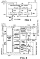
- FIG. 2 An architecture of a programmable logic controller (PLC) 10 according to the present invention is illustrated in Fig. 2.
- a fuse-programmble combinatorial logic circuit 12 receives input signals from an external source via a set of eight signal lines 14.
- various signal lines are hashmarked, with a numeral adjacent thereto, indicating that a number of signals are conducted in parallel on the line, even though only one line is shown, the numeral specifying the number of parallel signals.
- line 14 has the numeral "8" adjacent to a hashmark intersecting line 14.
- the programmable combinatorial logic circuit 12 can be formed from programmable AND and OR arrays as will be described in detail hereinafter.
- a set of twelve output macrocells 16 receives signals generated by circuit 12 via signal lines 18, as does a set of four buried registers 20 via signal lines 22.
- a programmable counter 24 also receives signals generated by circuit 12 via signal lines 26. These signals represent load address and counting control information, as will be described in detail below in connection with counter 24. Signals representing the contents of the buried registers 20 and the program counter 24 are conducted back, via signal lines 28, to the programmable combinatorial circuit 12 where they form a second input to circuit 12.
- Signals representing the contents of output macrocells 16 are conducted via signal lines 30 to input/output (I/O) pins 32 as well a being conducted back via signal lines 34 to combinatorial circuit 12 where they form a third input to circuit 12.
- the counter 24 is preferably a Gray-code counter. Since the contents of such a counter changes in only one bit location, state transitions are not subject to instabilities which may cause transient errors in the signals generated at I/O pins 32. Furthermore, this results in improved optimization of the Boolean design equations, since adjacent state product terms involve differences of only one bit, as will be appreciated by those skilled in the art.
- data signals and dynamic control signals generated by the combinatorial logic circuit 12 are conducted to each of the output macrocells 16 and the macrocell generates a signal therefrom which may be selected from the contents of a register within macrocell 16, or the combinatorial data signal received from circuit 12 and causes this signal, in either an active H1GH or active LOW polarity to be conducted to I/O pin 32 for output and feedback to circuit 12, or the macrocell may cause a signal applied at I/O pin 32 to be conducted via signal lines 30 and 34 to the logic circuit 12.
- Each buried register 20 also receives data and dynamic control signals from the logic circuit 12 but is not allocated an I/O pin on which the contents of the register can be generated, however, a signal representing the contents of the register is conducted via feedback path 28 to the logic circuit 12 where it can be used for "state" determination.
- the contents of the program counter 24 is similarly fedback to the logic circuit 12 for use in "state" determination and, since the external input signals are also available for logic circuit 12, implementation of both a "Mealy” state machine, in which the next-state determination is based on the current state and the inputs, and a "Moore” state machine, based solely on the current state, is readily performed by the PLC 10 of the present invention.
- the counter 24 can also perform sequencing functions and is readily controlled via the programmable logic circuit 12.
- the counter 24 receives a LOAD CONTROL signal generated by circuit 12 and a set of LOAD ADDRESS signals which, upon application of the LOAD CONTROL signal, permits setting of the contents of counter 24 to a programmable "state".
- Counter 24 can function as a set of extra buried registers.
- Counter 24 also receives a COUNTER CLEAR (CLR) signal from logic circuit 12, which, when asserted, resets the counter to a predetermined "start" state, such as "OO"Hex.
- CLR COUNTER CLEAR
- microsequencers employ a pipeline register with an instruction field which defines the branch address.
- the AND array is not programmable in a PROM-based microsequencer, a separate branch field and program counter are required.
- the programmable logic circuit 12 performs instruction decoding and branch control signals can be generated by the circuit 12 itself.
- LOAD ADDRESS and LOAD control signals can be generated directly for use by the program counter 24 of the PLC 10 instant invention.
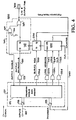
- a particular implementation of a PLC 100, a programmable AND array 122 and a pair of programmable OR arrays 124 and 126 form the programmable combinatorial logic circuit 120, corresponding to the logic circuit 12 in Fig. 2.
- Such a combinatorial logic circuit is referred to as a programmable logic array (PLA) in the art.
- Numerals of elements in Fig. 3 have a suffix of "0" appended to the numeral of the like element in Fig. 2.
- the programmable AND array 122 receives the external inputs via signal lines 140 terminating at a buffer 128 providing true and complemented versions of the external input signals conducted to the AND array 122.
- An "output generation" OR array 124 receives so-called “product term” signals from AND array 122 and generates therefrom data and dynamic control signals received via signal lines 180 by a register 162 within the output macrocells 160.
- a "control sequencing" OR array 126 receives product term signals from AND array 122 and generates therefrom data and dynamic control signals received via signal lines 220 by the buried registers 200, and LOAD ADDRESS signals and LOAD CONTROL signals received via signal lines 262 and 264, respectively, by the counter 240.
- the COUNTER clear (CLR) signal is also generated by OR array 126 and received via signal line 266 by counter 240.
- An output enable signal generated by AND array 122 is conducted to a first input terminal of an exclusive OR (XOR) gate 164.
- a field-programmable fusible link 166 is connected to a second input terminal of XOR gate 164.
- the status of fuse 166, blown or intact, determines the polarity of the output enable signal conducted to a control input terminal of an inverting output buffer 168.
- Buffer 168 receives the signal generated by register 162 and upon reception of the output enable signal, causes the contents of register 162 to be conducted at an output terminal of buffer 168.
- the signal so-generated is conducted to the I/O pin 320 and to the AND array 122, via feedback path 340.
- the contents of the buried registers 200 and the counter 240 are aso conducted to the AND array 122, via feedback path 340.
- Path 340 terminates at a buffer 129 providing true and complemented versions of the feedback signals for the AND array 122.
- inverting output buffer 168 If inverting output buffer 168 is disabled, external signals applied at I/O pin 320 can be conducted via feedback path 340 to the AND array 122.
- the two OR arrays 124 and 126 provide distinct functions within the PLC 100.
- the output generation OR array 124 is used to generate "output" control signals dependent upon the "state" count and the input signals.
- the control sequencing OR array 126 is used to generate "internal" control signals for the buried register 200, the LOAD ADDRESS and the control signals, LOAD and CLR, for the counter 240. These two operations are essentially independent from one another, and thus provision of the two arrays reduces the size of the array in half, from that required by a single OR array, without adversely affecting the functionality of PLC 100.
- a clock not shown, provides a timing signal CLK received by the registers 162 and 200 and the counter 240, as will be appreciated by those skilled in the art.
- FIG. 4 An alternative embodiment of a PLC according to the instant invention, employing fixed OR gates is shown in Fig. 4.
- Such a combinatorial logic circuit is referred to as a programmable array logic (PAL) in the art.
- PAL programmable array logic
- Numerals of elements in Fig. 4 have a suffix of "0" appended to the numeral of the like element in Fig. 2 and elements common to Fig. 3 have the same numeral in Fig. 4.
- the programmable AND array 122 receives the external inputs via signal lines 140 terminating at a buffer 128 providing true and complemented versions of the external input signals conducted to the AND array 122.
- a set of "output generation” OR gates, of which one, 123, is shown, receives so-called "product term” signals from AND array 122 and generates therefrom data signals received via signal lines 180 by a register 162 within the output macrocells 160.
- a variable distribution of product terms is conducted to the OR gates, in this case, eight and ten.
- a set of "control sequencing" OR gates receive a variable number of product term signals from AND array 122 and generates therefrom data and dynamic control signals received via signal lines 220 by the buried registers 200, and LOAD ADDRESS signals and LOAD CONTROL signals received via signal lines 262 and 264, respectively, by the counter 240.
- the COUNTER clear CLR signal is also generated by OR gate 125d and received via signal line 266 by counter 240.
- An output enable signal generated by AND array 122 is conducted to a first input terminal of an exclusive OR (XOR) gate 164.
- a field-programmable fusible link 166 is connected to a second input terminal of XOR gate 164.
- the status of fuse 166, blown or intact, determines the polarity of the output enable signal conducted to a first input terminal of a NOR gate 169.
- NOR gate 169 receives at a second input terminal the signal generated by register 162 and upon reception of the output enable signal, causes the contents of register 162 to be conducted at an output terminal of NOR gate 169.
- the signal so-generated is conducted to the I/O pin 320 and to the AND array 122, via feedback path 340.
- the contents of the buried registers 200 and the counter 240 are aso conducted to the AND array 122, via feedback path 340.
- Path 340 terminates at a buffer 129 providing true and complemented versions of the feedback signals for the AND array 122.
- the two sets of OR gates 123 and 125a, 125b, 125c and 125d provide distinct functions within the PLC 400.
- the output generation OR gates 123 are used to generate "output" control signals dependent upon the "state" count and the input signals.
- the control sequencing OR gates 125a, 125b, 125c and 125d are used to generate "internal" control signals for the buried register 200, the LOAD ADDRESS and the control signals, LOAD and CLR, for the counter 240.
- a clock not shown, provides a timing signal CLK received by the registers 162 and 200 and the counter 240, as will be appreciated by those skilled in the art.
- the programming of a PLC device 10 of the instant invention is preferably done via high level language (HLL) constructs. Provision of the high level logic counter element 24 within the PLC 10 facilitates this programming and the consequent understandability of the resulting program.
- HLL high level language
- a signal may be held by using only one or two product terms generated within the PLA in conjunction with feedback signals.
- C-REG count register
- C-MUX count multiplexer
- the programmable AND array of the PLC eliminates the need for these elements, as well as their attendant liabilities. HOLD input and RELEASE input statements are also available which perform similar operations on input signals.
- the high level language constructs IF...THEN...ELSE, WHILE...DO, FOR...DO, CASE...OF, GOTO and GOTOR are available to users of the PLC because of the provision of the programmable AND array and the state counter.
- the programmable AND array permits multiway branching from a given state, as described hereinbefore; and the state counter provides a direct correlation between the machine-state as used to design the software sequencer program and the contents of the state counter.
- the architecture and the software syntax allow the designer to use system control signal names in the statements rather than predefined opcodes because of the predecoded Boolean expressions in software.
- the ENABLE, DISABLE, RESET, PRESET and PRELOAD statements are directly related to the PLC output buffer 168 and register elements.
- the former two statements being related to the output enable signal generated by the programmable AND array, as described hereinbefore in connection with XOR gate 164 and the latter three statements related to the resetting, presetting and preloading of output macrocells 16 and/or the buried registers 20, that, although not illustrated in the figures, can be provided by reference to our copending European Patent Application 86308372.1.
- the high level language constructs illustrated in the Table can be translated into Boolean expressions and then used directly in conjunction with any of a number of current PAL design specification languages, such as PLPL, ABEL or CUPL, to aid in the programming of the logic circuitry 12.
- PAL design specification languages such as PLPL, ABEL or CUPL
- Such constructs provide extensive control of instruction decode, conditional testing and branching.
- elements normally required in PROM-based microsequencers such as test multiplexers, test masks, program counter multiplexers, condition code multiplexers, and branch control logic circuits, are not required in a PLC 10 of the instant invention.
- the programmable counter 240 is provided for sequencing, state counting and control of the programmable AND array 122, through feedback path 340.
- the counter 240 is user-controlled via the programmable AND array 122 (and the control sequence OR array 126, in the embodiment of Fig. 3).
- the contents of counter 240 can be loaded from AND array 122 (OR array 126 of Fig. 3) and the resulting count used to represent a state, which in conjunction with the AND array 122 (and OR array 124 of Fig. 3) can be used in the generation of output signals by output macrocells 160.
- Loading of the counter 240 provides the branching function of the state machine.
- the clearing of the counter resets the counter 240 to 00 (Hex) which is the normal starting state of the state machine.
- control structure of a state machine or sequencer implemented by a PLC 100 of the instant invention is controlled by the AND-OR array 122 and 126 combination and is dependent on the present state of the machine, i.e., present contents of counter 240, the input signals to the AND array 122, and the output signals fedback to the AND array via path 340.
- a ten-bit counter 240 provides 1,024 states. However, additional states can be provided by using the contents of the buried registers 200 in determining the present state.
- a second major task in state machine design is the generation of the control output signals.
- output signals can readily be generated dependent on the state of the machine and the input signals. For example, suppose a state machine having the states 00 and 01 is to perform the following operation:
- conditional inputs is programmable in the PLC 100 by way of software and the programmable AND array.
- conditional testing can make use of any state(s), or be independent of state, can make use of any combination of inputs, can make use of outputs fedback to the AND array, and can be for any particular length of time.
- Branching is performed by the PLC of the present invention based on the programmable conditional inputs to the programmable AND array 122.
- Dependent on the present state, as reflected by the contents of counter 240, and the conditional inputs, a LOAD CONTROL signal, and a set of LOAD ADDRESS signals can be generated by the control sequence OR array 126. The latter set of signals representing the state to which a branch is desired.
- the contents of counter 240 will be set to the desired branch state and on subsequent clock cycles, the count will resume from this state onwards.
- branching operations can be implemented by the programmable counter 240 of PLC 100 as follows:
- LOAD CONTROL signal is denoted LOAD
- LS2 the set of LOAD ADDRESS signals
- the instructions for the PLC 10 of the present invention are predecoded by conversion into Boolean equations and stored in this functional logical form in the AND-OR array portion 12. Since the conversion is performed by software, any user-specified application-oriented instruction set can be performed on the PLC 10, unlike prior art PROM-based microsequencers in which a hardware element - a dedicated instruction decode PLA - is used to convert instructions. Furthermore, since the prior art PROM-based microsequencers must convert the instructions from a data format at execution time, such microsequencers operate more slowly than the PLC 10 of the instant invention.
Landscapes
- Engineering & Computer Science (AREA)
- Software Systems (AREA)
- Theoretical Computer Science (AREA)
- Physics & Mathematics (AREA)
- General Physics & Mathematics (AREA)
- General Engineering & Computer Science (AREA)
- Mathematical Physics (AREA)
- Automation & Control Theory (AREA)
- Logic Circuits (AREA)
- Programmable Controllers (AREA)
Abstract
Description
- The present invention relates to programmable logic devices, and more particularly, to such devices suitable for use in control applications, for instance, as sequencers, and having easily-programmable high level logic elements such as counters.
- Reference may be made to our copending European patent application 86308372.1 entitled "Programmable Input/Output Cell with Flexible Clocking and Flexible Feedback".
- The first step in designing a sequential digital circuit is to construct a "state diagram" indicating the state transitions and output signal resulting from the application of various input signals. A so-called "Moore" machine is one in which the output signals are dependent only on the state, while in a so-called "Mealy" machine, the output signals are dependent both on the state and the input signals. Presently, programmable array logic (PAL) devices, and programmable logic array (PLA) devices find application for controlling digital circuitry, such as in "state machines" or sequencers, requiring flexibility and ease of use.
- Although such PAL/PLA devices operate with speed and flexibility, they are difficult to program, since they require writing complex Boolean expressions for this purpose. The use of Boolean equations to design the sequencer limits the number of variables available to the designer to eight because of the mathematical difficulties in specifying and simplifying equations having typically more than eight variables. Moreover, such sequencers require additional external circuitry to provide flexibility as well as additional conditional input testing circuitry.
- Particular difficulty is encountered when programming and understanding a general PAL or PLA device used to perform higher level logical functions such as counting, state sequencing, branching, or multiple-case testing. No higher level logic blocks, especially program counters, are available in such devices which can be readily programmed or easily understood. The absence of these higher level logical blocks makes it very difficult to implement with PALs and PLAs sequencers and state machines with high level language-based state machine constructs. Also, lack of these high level logical blocks makes current PAL/PLA device architecture unoptimized for control logic applications.
- While to reduce programming effort and to ease understandability, some higher level language (HLL) programming schemes may be used, there is no direct relationship between such HLL constructs and the underlying hardware. As such, no methodology is available which affords easy design of the microsequencer (because no high level constructs are readily available within the PAL- or PLA-based sequencers) corresponding to the high level language constructs most useful to design personnel. Complex, detailed and error-prone Boolean equations must be written presently to accomplish the design of PAL- or PLA-based sequencers. Such equations do not bear a one-to-one correspondence to the underlying circuit elements of the PAL- or PLA-based sequencer. Because of all these reasons, PAL/PLA devices are not used for large complex control applications.
- Usually, programmable read-only memory (PROM)-based micro-coded sequencers are used for such control applications. One such device is illustrated in block diagram form in Fig. 1. However, such microsequencers have many deficiencies. For instance, to implement "conditional testing" for the construction of Moore and Mealy state machines, requires the use of a dedicated testing multiplexer (TEST MUX) element. However, the TEST MUX can use only one of the conditional test inputs it receives to determine the next state. Accordingly, in PROM-based microsequencers, it is not possible to perform multiple conditional testing in a single clock cycle. For example, to implement the following test at a state n:
STATE_n: IF (COND1) THEN OUTPUT X, IF (COND2) THEN OUTPUT Y; a PROM-based microsequencer requires two (sub) states, each testing a single condition:
STATE_n1: IF (COND1) THEN OUTPUT X;
STATE_n2: IF (COND2) THEN OUTPUT Y; - The resulting code is more complicated and slower to execute than need be, as it requires two clock cycles. Further, PROM-based microsequencers allow only state-dependent conditional testing. It is very difficult to perform state-independent conditional testing or conditional testing based on only a partial number of states, without wasting so-called "product terms", since PROM-based microsequencers allow only one product term per state.
- For instance, the following example employs multiple condition testing for states n and n+1 only, i.e., a partial number of states:
STATE_n: IF (COND1) THEN OUT1, IF INITL THEN BOOT;
STATE_n+1: OUT1, OUT11, IF INITL THEN BOOT;
.
.
.
STATE_n+m: GOTO m;
This example cannot be implemented in PROM-based microsequencers. - As a second example, the following instruction requires that if the "global" input INITL is asserted, the state machine should branch to START, independent of the present state:
IF (INITL) GOTO STATE (START); - This instruction is an example of state-independent branching and can only be implemented in micro-interruptible PROM-based microsequencers. This requires additional circuitry (not shown in Fig. 1) and imposes an undesirabale "exception-handling" technique for what should be a relatively straightforward state-independent operation.
- Frequently, in microsequencer design, it is desirable to provide multiple branches from a given state to different states on different conditional input signals. In PROM-based microsequencers additional circuitry must be provided to perform this function. In PROM-based microsequencers, such as shown in Fig. 1, all product terms are predecoded. The designer is therefore limited to branches to only one location at a time. PROM-based microsequencers do not directly provide genuine "multiway" branching capability. Extra hardware elements, such as the BRANCH CONTROL LOGIC (GOTO) element shown in Fig. 1, used in conjunction with masking, is needed to provide limited multiway branching. The branching address is derived from the conditional (test) inputs along with a user-definable mask. This provides a jump to only a limited number of states selectable by masking of the inputs being tested as provided by the bit-by-bit "AND" function.
- For example, to implement the multiway branch STATE_n IF (COND1) THEN OUT2, IF (COND2) THEN OUT2; requires in a PROM-based microsequencer the statements
STATE_n GOTO (CONDITIONAL INPUTS "AND" MASK)
.
.
.
STATE_m OUT1
STATE_p OUT2
in which the MASK is chosen to cause generation of the address for STATE_m when the CONDITIONAL INPUTS correspond to COND1, and for STATE_p when the CONDITONAL INPUTS correspond to COND2. - As will be appreciated by those skilled in the art, such techniques undesirably complicate the design of the microsequencer, and in any case, additional conditonal testing circuitry must be provided to perform these operations. Such circuitry takes valuable die area, leads to slower execution times, and makes sequencer design cumbersome.
- In PROM-based microsequencers, as can be seen from the above discussion, "multiway" branching from a state can only be performed by executing either a series of single jumps or with additional logic circuitry. Such a limitation violates good structured program design which uses such high level language constructs as the IF THEN ELSE and CASE. Furthermore, such limitation slows execution times and makes program verification and documentation difficult.
- In PROM-based microsequencers, instructions are stored in a logical data form:
OPCODE, COND_SELECT, BRANCH ADDRESS, OUTPUT.
Instruction decoding in PROM-based microsequencers is accomplished at execution-time by MICROINSTRUCTION DECODE PLA which is hardwired to the various elements of the microsequencer shown in Fig. 1. This PLA receives the operation code (opcode) of an instruction from the pipeline register, decodes it, and generates, over time, a series of control signals which cause the various elements within the microsequencer, such as the branch control logic, test multiplexer, program counter multiplexer (PC MUX), microprogram PROM, pipeline register, shift registers, and the like, to undertake and coordinate their respective functions. Also, in PROM-based microsequencers, separate instruction decode logic circuitry is required and the user is restricted to the fixed instruction operation codes defined by the manufacturer of the device. The fixed-instruction decode PLA severely limits the flexibility of usage, and imposes additional instruction decoding time for each microcycle. PROM-based microsequencers have fixed AND arrays to perform addressing. The overall performance and speed of the microsequencer of Fig. 1 is thereby degraded. - Similar to conditional testing and branching, instruction execution is also state dependent only. PROM-based microsequencers do not provide state independent conditional testing, branching or instruction decoding.
- Furthermore, even when specific output signals do not change for several clock cycles, the output signal must be held constant. In PROM-based microsequencers, this requirement means that product terms are generated every clock cycle thereby wasting PROM product terms. Also PROM-based microsequencers waste product terms when executing branches.
- Further, no internal feedback paths are provided to apply output signals generated by PROM-based microsequencers to the PROM array. Also every state product term drives all the outputs of a PROM-based microsequencer which has an adverse affect on the speed of the device.
- In summary, PROM-based microsequencers do not provide adequate high level constructs for state machine/sequencer design, limit design instructions to one construct per line, and impose fixed opcodes thus making customization of user-specific software difficult. Their architecture, while related, is not optimized to the higher level constructs which designers prefer to use.
- Various programmable logic devices of the general type to which the present invention relates are described in a paper entitled "Programmable logic chip rivals gate arrays in flexibility" by B. Kitson et al - Electronic Design, 8 December 1983 and in a paper entitled "Next Generation Programmable Logic" - Wescon Technical Papers, 30 October 1984.
- We will describe a programmable logic controller (PLC) device having high level circuit elements which can be used in conjunction with a design methodology allowing developments of software having high-level language constructs for programming the controller, the constructs bearing a one-to-one relationship to the underlying architecture of the PLC device.
- We will describe an arrangement which employs architecture providing faster instruction sequencing than is available from PROM-based microsequencers.
- We will describe an arrangement which allows development of software sequencing customized to particular applications.
- We will employ an architecture enhancing fast control sequencing by eliminating stages in the instruction execution cycle, such as instruction decode.
- The described arrangement will eliminate circuit elements required in PROM-based microsequencers, such as test multiplexers, instruction decode PLA, counter multiplexers, and the like.
- The programmable logic controller (PLC) to be described is specifically tailored for control applications both from the functionality and usage point of view. The PLC offers substantial advantages over the conventional PALs/PLAs and PROM-based microsequencers used for control applications. It offers a generic superset of PROM-based microsequencer functionality and flexibility. Also it provides for the use of higher level language constructs, in place of boolean equations or microcode. It is actually a "software sequencer" as its instruction decode is programmable in software. Also for the same functionality, the PLC device requires less silicon, and offers higher speed than PROM-based microsequencers.
- In a PLC, a set of output registers along with a counter and a set of general purpose buried registers constitute the counterpart to the pipeline register of PROM-based microsequencers. The counter in a PLC design provides the functionality analogous to a program counter in the PROM-based microsequencer design. It also provides the jump address field of the PROM-based microsequencer pipeline register. Further, in the described PLC device, a programmable AND array, performs the addressing functions of PROM-based microsequencers. In the PLC described, these combinations provide extra flexibility in control and reduced silicon die area as the AND array is programmable, and the jump address needs to be generated only when required.
- The extra logic circuitry required in a PROM-based microsequencer, such as a program counter multiplexer branch control logic, test multliplexer, instruction decode, and count register, is not required in a PLC. In addition to addressing, the AND array performs instruction decode, conditional testing, branch address generation and a number of miscellaneous functions. The described PLC inherently provides a superset of the functionality provided by these redundant logic blocks in microsequencers. The PLC provides improved functionality, ease of use, faster speeds and lesser silicon for the same functionality as compared to prior art microsequencers.
- Provided in one embodiment of a programmable logic controller of the instant invention, is a combinatorial logic circuit comprising a programmable AND array and a pair of programmable OR arrays. A first OR array generates logic signals to a set of output macrocells served by a set of input/output pins. A second OR array generates logic signals to a set of "buried" internal registers and a counter. The second OR array provides a high level logic control sequencing function. The signals generated by certain ones of the output macrocells as well as the internal registers and the counter are fedback to the AND array via dedicated internal feedback paths.
- In the described PLC, "conditional testing" is performed within the programmable AND array, and therefore is entirely user-determinable. Any set of product terms may be specified by the user in the design of Moore or Mealy state machines. Furthermore, because such testing is done by the AND array, no additonal circuitry, nor the accompanying complexity, die size and time penalties, is present in the described PLC.
- Because of the flexibility of this conditional testing, software sequencing is more transparent and quicker executing. For instance, where a PROM-based microsequencer may require three states to perform the requisite testing, the described PLC only requires one state.
- Provision of a counter within the PLC allows the "product terms" (states), generated by the AND array to be based on the contents of both the counter as well as the input signals. Furthermore, the resulting conditional testing capability of the PLC eliminates the need for a test multiplexer, a test mask, the program counter multiplexer, the control multiplexer and the branch control logic which also saves die area. In addition, the PLC affords state-dependent, state-independent and partial-state-dependent multiple conditional branching.
- The described PLC supports true multiway branching because of the presence of the programmable AND array. Provision of the counter, in conjunction with the product terms generated by the AND array, permits multiple next-state product terms to be generated thereby from a single present state. High level language constructs such as IF THEN ELSE and CASE can be employed by the designer to take advantage of this architecture. The resulting code will bear a direct relationship to the underlying architecture and accordingly will be easier to develop and be more readily understood and documented when completed. In addition, relative branching, branch to location defined by input signals, and interrupts are readily implemented in the described PLC because of provision of the user-programmable AND array.
- The PLC provides the capability of multiple branching on multiple test conditions without the additional branch control logic, test multiplexer, and the like, of the prior art PROM-based microsequencers. As instruction decoding is performed in the user-programmable AND array, the decoding of each instruction can be specified in software by the designer. Hence in the PLC device, instructions are predecoded according to their software specification and stored in the AND array in a logical format directly usable by the hardware. This is far more efficient than storing instructions in the PROM microprogram memory in a data format and utilizing a separate instruction decode PLA to decode them. Thus the PLC device eliminates the need for the dedicated instruction decode PLA of the prior art, and results in savings in die area, instruction execution time and offers substantial flexibility. With the PLC device, the designer can use software having high-level constructs which are easy to comprehend and do not impose unnecessary restrictions such as requiring typically no more than eight to sixteen variables in Boolean design expressions.
- Because of the provision of the programmable AND array, the PROM-based microsequencer's restriction of one instruction per state is not imposed by the described PLC. Instructions corresponding to a particular state may be cascaded and instruction sequences may be customized and/or optimized by the user for particular applications. Hence, a PLC will perform instruction sequences more quickly than a PROM-based sequencer and the resulting code will be easy to understand. Furthermore, most PROM-based microsequencers require an instruction field within the pipeline register for storing a branch address. As these sequencers have no programmable AND array, the separate branch field and a program counter are required for branching control. In a PLC, the provision of the programmable AND array allows branch control signals to be generated within the AND array and because of the presence of the counter having load control signals generated by the programmable OR array, the PLC does not need a separate branch field and program counter, resulting in saving of die area and a more transparent architecture.
- The PLC which we will describe, provides dedicated feedback paths from the output terminals and output macrocells. The feedback paths eliminate this need for separate product terms for each state for implementing hold, release, and delay functions, thereby saving product terms. Further, the signals generated at the outputs of the PLC can be either registered or combinatorial, active HIGH or active LOW. These capabilities are not available in prior art PROM-based microsequencers. The capability of combinatorial outputs allows both Mealy and Moore type state machine designs, whereas prior art PROM-based microsequencers implement only Moore type state machines.
- Because PROM-based sequencers use a fully predecoded AND array, output signals generated thereby cannot be independent of state. "Interruptible" microsequencers are sometimes constructed to provide limited state-independent functions, by employing excessive external circuitry. The provision of a user-programmable AND array in the PLC of the instant invention permits providing state-independent functions and partial-state dependent functions, without the use of complex interrupt-driven opcodes and external circuitry.
- By providing a programmable AND array in the PLC receiving external input signals, feedback signals, and state count signals, the additional information supplied in PROM-based sequencers, such as the use of a conditional test multiplexer, the opcode and constant instruction fields, are unnecessary. The AND array can be programmed, in conjunction with the programmable OR array, to generate the required control signals. Furthermore, the number of OR terms dependent on a single product term is quite critical. For enhanced speed, it is important to reduce the size of the OR array so as to eliminate the second gate delay as much as possible. The described PLC employs two OR arrays, each performing a dedicated function, either output generation, or sequencer control, thereby reducing the size of each OR array without loss of functionality.
- In an alternative embodiment, a faster PLC employs a combinatorial logic circuit comprising a programmable AND array and fixed OR arrays.
- Fig. 1 is a block diagram of a PROM-based microsequencer of the prior art.
- Fig. 2 illustrates the architecture of a programmable logic controller (PLC) according to the instant invention.
- Fig. 3 is a block diagram of an embodiment of a PLC having a programmable AND array and a pair of programmable OR arrays.
- Fig. 4 is a block diagram of an embodiment of a PLC having a programmable AND array and fixed OR gates.
- An architecture of a programmable logic controller (PLC) 10 according to the present invention is illustrated in Fig. 2. A fuse-programmble
combinatorial logic circuit 12 receives input signals from an external source via a set of eightsignal lines 14. On the drawing figures, various signal lines are hashmarked, with a numeral adjacent thereto, indicating that a number of signals are conducted in parallel on the line, even though only one line is shown, the numeral specifying the number of parallel signals. Accordingly,line 14 has the numeral "8" adjacent to ahashmark intersecting line 14. The programmablecombinatorial logic circuit 12 can be formed from programmable AND and OR arrays as will be described in detail hereinafter. - A set of twelve
output macrocells 16 receives signals generated bycircuit 12 viasignal lines 18, as does a set of four buried registers 20 via signal lines 22. - A
programmable counter 24 also receives signals generated bycircuit 12 via signal lines 26. These signals represent load address and counting control information, as will be described in detail below in connection withcounter 24. Signals representing the contents of the buried registers 20 and theprogram counter 24 are conducted back, viasignal lines 28, to the programmablecombinatorial circuit 12 where they form a second input tocircuit 12. - Signals representing the contents of
output macrocells 16 are conducted viasignal lines 30 to input/output (I/O) pins 32 as well a being conducted back viasignal lines 34 tocombinatorial circuit 12 where they form a third input tocircuit 12. Thecounter 24 is preferably a Gray-code counter. Since the contents of such a counter changes in only one bit location, state transitions are not subject to instabilities which may cause transient errors in the signals generated at I/O pins 32. Furthermore, this results in improved optimization of the Boolean design equations, since adjacent state product terms involve differences of only one bit, as will be appreciated by those skilled in the art. - Briefly, data signals and dynamic control signals generated by the
combinatorial logic circuit 12 are conducted to each of theoutput macrocells 16 and the macrocell generates a signal therefrom which may be selected from the contents of a register withinmacrocell 16, or the combinatorial data signal received fromcircuit 12 and causes this signal, in either an active H1GH or active LOW polarity to be conducted to I/O pin 32 for output and feedback tocircuit 12, or the macrocell may cause a signal applied at I/O pin 32 to be conducted viasignal lines logic circuit 12. Each buried register 20, also receives data and dynamic control signals from thelogic circuit 12 but is not allocated an I/O pin on which the contents of the register can be generated, however, a signal representing the contents of the register is conducted viafeedback path 28 to thelogic circuit 12 where it can be used for "state" determination. - The contents of the
program counter 24 is similarly fedback to thelogic circuit 12 for use in "state" determination and, since the external input signals are also available forlogic circuit 12, implementation of both a "Mealy" state machine, in which the next-state determination is based on the current state and the inputs, and a "Moore" state machine, based solely on the current state, is readily performed by thePLC 10 of the present invention. Thecounter 24 can also perform sequencing functions and is readily controlled via theprogrammable logic circuit 12. Thecounter 24 receives a LOAD CONTROL signal generated bycircuit 12 and a set of LOAD ADDRESS signals which, upon application of the LOAD CONTROL signal, permits setting of the contents ofcounter 24 to a programmable "state". Loading of the counter in this manner provides a "state branching" function of thePLC 10. Alternatively, by permanently setting the LOAD CONTROL signal HIGH, thecounter 24 can function as a set of extra buried registers.Counter 24 also receives a COUNTER CLEAR (CLR) signal fromlogic circuit 12, which, when asserted, resets the counter to a predetermined "start" state, such as "OO"Hex. - Most microsequencers employ a pipeline register with an instruction field which defines the branch address. As the AND array is not programmable in a PROM-based microsequencer, a separate branch field and program counter are required. In a
PLC 10 of the instant invention, theprogrammable logic circuit 12 performs instruction decoding and branch control signals can be generated by thecircuit 12 itself. As such, LOAD ADDRESS and LOAD control signals can be generated directly for use by theprogram counter 24 of thePLC 10 instant invention. - With reference to Fig. 3, a particular implementation of a
PLC 100, a programmable ANDarray 122 and a pair of programmable ORarrays combinatorial logic circuit 120, corresponding to thelogic circuit 12 in Fig. 2. Such a combinatorial logic circuit is referred to as a programmable logic array (PLA) in the art. - Numerals of elements in Fig. 3 have a suffix of "0" appended to the numeral of the like element in Fig. 2. As shown in Fig. 3, the programmable AND
array 122 receives the external inputs viasignal lines 140 terminating at abuffer 128 providing true and complemented versions of the external input signals conducted to the ANDarray 122. An "output generation" ORarray 124 receives so-called "product term" signals from ANDarray 122 and generates therefrom data and dynamic control signals received viasignal lines 180 by aregister 162 within theoutput macrocells 160. A "control sequencing" ORarray 126 receives product term signals from ANDarray 122 and generates therefrom data and dynamic control signals received via signal lines 220 by the buriedregisters 200, and LOAD ADDRESS signals and LOAD CONTROL signals received viasignal lines 262 and 264, respectively, by thecounter 240. The COUNTER clear (CLR) signal is also generated by ORarray 126 and received viasignal line 266 bycounter 240. - An output enable signal generated by AND
array 122 is conducted to a first input terminal of an exclusive OR (XOR)gate 164. A field-programmable fusible link 166 is connected to a second input terminal ofXOR gate 164. The status of fuse 166, blown or intact, determines the polarity of the output enable signal conducted to a control input terminal of an invertingoutput buffer 168.Buffer 168 receives the signal generated byregister 162 and upon reception of the output enable signal, causes the contents ofregister 162 to be conducted at an output terminal ofbuffer 168. The signal so-generated is conducted to the I/O pin 320 and to the ANDarray 122, viafeedback path 340. The contents of the buriedregisters 200 and thecounter 240 are aso conducted to the ANDarray 122, viafeedback path 340.Path 340 terminates at abuffer 129 providing true and complemented versions of the feedback signals for the ANDarray 122. - If inverting
output buffer 168 is disabled, external signals applied at I/O pin 320 can be conducted viafeedback path 340 to the ANDarray 122. - The two OR
arrays PLC 100. The output generation ORarray 124 is used to generate "output" control signals dependent upon the "state" count and the input signals. The control sequencing ORarray 126 is used to generate "internal" control signals for the buriedregister 200, the LOAD ADDRESS and the control signals, LOAD and CLR, for thecounter 240. These two operations are essentially independent from one another, and thus provision of the two arrays reduces the size of the array in half, from that required by a single OR array, without adversely affecting the functionality ofPLC 100. - A clock, not shown, provides a timing signal CLK received by the
registers counter 240, as will be appreciated by those skilled in the art. - An alternative embodiment of a PLC according to the instant invention, employing fixed OR gates is shown in Fig. 4. A
PLC 400, a programmable ANDarray 122 and a set of ORgates combinatorial logic circuit 120, corresponding to thelogic circuit 12 in Fig. 2. Such a combinatorial logic circuit is referred to as a programmable array logic (PAL) in the art. - Numerals of elements in Fig. 4 have a suffix of "0" appended to the numeral of the like element in Fig. 2 and elements common to Fig. 3 have the same numeral in Fig. 4. As shown in Fig. 4, the programmable AND
array 122 receives the external inputs viasignal lines 140 terminating at abuffer 128 providing true and complemented versions of the external input signals conducted to the ANDarray 122. A set of "output generation" OR gates, of which one, 123, is shown, receives so-called "product term" signals from ANDarray 122 and generates therefrom data signals received viasignal lines 180 by aregister 162 within theoutput macrocells 160. A variable distribution of product terms is conducted to the OR gates, in this case, eight and ten. - A set of "control sequencing" OR gates, of which four, 125a, 125b, 125c and 125d are shown, receive a variable number of product term signals from AND
array 122 and generates therefrom data and dynamic control signals received via signal lines 220 by the buriedregisters 200, and LOAD ADDRESS signals and LOAD CONTROL signals received viasignal lines 262 and 264, respectively, by thecounter 240. The COUNTER clear CLR signal is also generated by OR gate 125d and received viasignal line 266 bycounter 240. - An output enable signal generated by AND
array 122 is conducted to a first input terminal of an exclusive OR (XOR)gate 164. A field-programmable fusible link 166 is connected to a second input terminal ofXOR gate 164. The status of fuse 166, blown or intact, determines the polarity of the output enable signal conducted to a first input terminal of a NORgate 169. NORgate 169 receives at a second input terminal the signal generated byregister 162 and upon reception of the output enable signal, causes the contents ofregister 162 to be conducted at an output terminal of NORgate 169. The signal so-generated is conducted to the I/O pin 320 and to the ANDarray 122, viafeedback path 340. The contents of the buriedregisters 200 and thecounter 240 are aso conducted to the ANDarray 122, viafeedback path 340.Path 340 terminates at abuffer 129 providing true and complemented versions of the feedback signals for the ANDarray 122. - If NOR
gate 169 is disabled, external signals applied at I/O pin 320 can be conducted viafeedback path 340 to the ANDarray 122. - The two sets of OR
gates PLC 400. The output generation ORgates 123 are used to generate "output" control signals dependent upon the "state" count and the input signals. The control sequencing ORgates 125a, 125b, 125c and 125d are used to generate "internal" control signals for the buriedregister 200, the LOAD ADDRESS and the control signals, LOAD and CLR, for thecounter 240. These two operations are essentially independent from one another, and thus provision of the two sets of gates reduces the number of gates, while the speed ofPLC 400 is markedly increased compared with that ofPLC 100. - A clock, not shown, provides a timing signal CLK received by the
registers counter 240, as will be appreciated by those skilled in the art. - The programming of a
PLC device 10 of the instant invention is preferably done via high level language (HLL) constructs. Provision of the high levellogic counter element 24 within thePLC 10 facilitates this programming and the consequent understandability of the resulting program. An exemplary syntax is shown in the accompanying table.
- The meaning of most of the simple statements shown in the Table are self-explanatory to those skilled in the art. For instance, reference can be had to Chapter 4, "Design and Software for Programmable Logic", in the Programmable Array Logic Handbook by Advanced Micro Devices, Sunnyvale, CA c 1984. However, because of the various advantages of the PLC of the instant invention, several high level language constructs are supported by the PLC which are unavailable in the prior art. For example, the DELAY statement provides holding the signal generated at the output of the PLC constant for a specified number of clock cycles. In PROM-based sequencers, since all states are predecoded and the output signals are generated automatically at each clock cycle. Because of the presence of feedback paths in the PLC, a signal may be held by using only one or two product terms generated within the PLA in conjunction with feedback signals. In some prior art sequencers (see Fig. 1), a separate count register (C-REG) and count multiplexer (C-MUX) is used to provide the hold function, thereby requiring extra die area and circuit complexity as well as programming complexity. The programmable AND array of the PLC eliminates the need for these elements, as well as their attendant liabilities. HOLD input and RELEASE input statements are also available which perform similar operations on input signals.
- The high level language constructs IF...THEN...ELSE, WHILE...DO, FOR...DO, CASE...OF, GOTO and GOTOR are available to users of the PLC because of the provision of the programmable AND array and the state counter. The programmable AND array permits multiway branching from a given state, as described hereinbefore; and the state counter provides a direct correlation between the machine-state as used to design the software sequencer program and the contents of the state counter. Furthermore, the architecture and the software syntax allow the designer to use system control signal names in the statements rather than predefined opcodes because of the predecoded Boolean expressions in software. These constructs are not available in the prior art because of their lack of high level elements.
- The ENABLE, DISABLE, RESET, PRESET and PRELOAD statements are directly related to the
PLC output buffer 168 and register elements. The former two statements being related to the output enable signal generated by the programmable AND array, as described hereinbefore in connection withXOR gate 164 and the latter three statements related to the resetting, presetting and preloading ofoutput macrocells 16 and/or the buried registers 20, that, although not illustrated in the figures, can be provided by reference to our copending European Patent Application 86308372.1. - The high level language constructs illustrated in the Table can be translated into Boolean expressions and then used directly in conjunction with any of a number of current PAL design specification languages, such as PLPL, ABEL or CUPL, to aid in the programming of the
logic circuitry 12. In particular, such constructs provide extensive control of instruction decode, conditional testing and branching. As such, elements normally required in PROM-based microsequencers, such as test multiplexers, test masks, program counter multiplexers, condition code multiplexers, and branch control logic circuits, are not required in aPLC 10 of the instant invention. - To further understand the benefits and advantages of a
PLC 10 according to the instant invention, five illustrative control tasks using the PLC will now be described: control sequencing, output generation, conditonal testing, branching, and instruction decode. - The
programmable counter 240 is provided for sequencing, state counting and control of the programmable ANDarray 122, throughfeedback path 340. In turn, thecounter 240 is user-controlled via the programmable AND array 122 (and the control sequence ORarray 126, in the embodiment of Fig. 3). The contents ofcounter 240 can be loaded from AND array 122 (ORarray 126 of Fig. 3) and the resulting count used to represent a state, which in conjunction with the AND array 122 (and ORarray 124 of Fig. 3) can be used in the generation of output signals byoutput macrocells 160. - Hence, both Mealy and Moore type state machines are readily implemented by a
PLC 100 of the instant invention. As the operation ofcounter 240 is normally sequential, the operation of the state machine is easier to comprehend and program in software than the PAL sequencers of the prior art. - Loading of the
counter 240 provides the branching function of the state machine. The clearing of the counter resets thecounter 240 to 00 (Hex) which is the normal starting state of the state machine. - Accordingly, the control structure of a state machine or sequencer implemented by a
PLC 100 of the instant invention is controlled by the AND-ORarray counter 240, the input signals to the ANDarray 122, and the output signals fedback to the AND array viapath 340. - In a representative embodiment, a ten-
bit counter 240 provides 1,024 states. However, additional states can be provided by using the contents of the buriedregisters 200 in determining the present state. - A second major task in state machine design is the generation of the control output signals. By virtue of the programmable AND-OR
arrays 12 within thePLC 10 of the instant invention, output signals can readily be generated dependent on the state of the machine and the input signals. For example, suppose a state machine having the states 00 and 01 is to perform the following operation:
- By encoding the states 00 and 01, as
S0 ,S1 andS2 ; and S0,S1 andS2 , respectively, where S0, S1 and 52 represent the signals generated bycounter 240, output signals 01 and 03 can be generated according to the following equations, dependent on signals S0, S1, S2 and their complements and the input signal I3:
and
- These latter equations are readily imlemented by the programmable AND-
OR array 12, as will be appreciated by those skilled in the art. - The selection of conditional inputs is programmable in the
PLC 100 by way of software and the programmable AND array. The conditional testing can make use of any state(s), or be independent of state, can make use of any combination of inputs, can make use of outputs fedback to the AND array, and can be for any particular length of time. - For example, in a state machine having the states 04 and 05 performing the following conditional testing operations on the input signals
MREQ ,CS andRAS :
- By encoding the states 04 and 05 as
S0 ,S1 and S2; and S0,S1 and S2, respectively, the conditional testing operations can be implemented by thePLC 10 as:
and
- Branching is performed by the PLC of the present invention based on the programmable conditional inputs to the programmable AND
array 122. Dependent on the present state, as reflected by the contents ofcounter 240, and the conditional inputs, a LOAD CONTROL signal, and a set of LOAD ADDRESS signals can be generated by the control sequence ORarray 126. The latter set of signals representing the state to which a branch is desired. During the next clock cycle, the contents ofcounter 240 will be set to the desired branch state and on subsequent clock cycles, the count will resume from this state onwards. - For example, suppose it is desired to perform the following branching operations:

- Continuing with the state-encoding use in the previous examples, these branching operations can be implemented by the
programmable counter 240 ofPLC 100 as follows: - LOAD =
-
S2 *S1 *S0 +CS *S2 *S1 *S0 + CS *S2 *S1 * S0 - LS2 =
- 0
- LS1 =
-
S2 *S1 *S0 - LS0 =
-
S2 *S1 *S0 +S2 *S1 * S0 * CS - In which the LOAD CONTROL signal is denoted LOAD and the set of LOAD ADDRESS signals are denoted LS2, LS1 and LS0, from most-significant to least-significant, respectively.
- As described above, in connection with the
counter 240, a dedicated clear function is provided for the counter. Application of the COUNTER CLR signal will cover the contents ofcounter 240 to be set to ZERO, or another predetermined value, representing the "start" state. An extension of the branching example to perform a "return to start" operation will now be clear to those skilled in the art. - The instructions for the
PLC 10 of the present invention are predecoded by conversion into Boolean equations and stored in this functional logical form in the AND-OR array portion 12. Since the conversion is performed by software, any user-specified application-oriented instruction set can be performed on thePLC 10, unlike prior art PROM-based microsequencers in which a hardware element - a dedicated instruction decode PLA - is used to convert instructions. Furthermore, since the prior art PROM-based microsequencers must convert the instructions from a data format at execution time, such microsequencers operate more slowly than thePLC 10 of the instant invention.
Claims (41)
- A programmable logic controller comprising a logic device having a plurality of inputs (14,140) and a plurality of outputs (I/O), comprising:
programmable logic means (12,120) responsive to input signals applied to a number of said inputs (14,140) to generate a plurality of programmably defined logic signals;
characterised by counter means (24,240) arranged to receive a first number of said programmably defined logic signals, to store a count address derived from the first number of logic signals, and to generate therefrom a sequence of output address signals based on that count address;
wherein the first number (26,262-266) of logic signals includes one or more control signals (264,266) for selectively instructing the counter means (24,240) to either maintain a current count address or to load a new count address defined by the first number (26,262-266) of logic output signals, the loading of a new count address causing each subsequent count address to be a derivation of the loaded new count address. - A programmable logic controller according to Claim 1, characterised in that said counter means is arranged to generate a sequence of output address signals in response to a system clock signal (CLK) applied to the counter means and to other portions (200,162) of the device.
- A programmable logic controller according to Claim 2, characterised in that said counter means is arranged to selectably increment or decrement said address in response to said clock signals.
- A programmable logic controller according to Claim 1, 2 or 3, characterised in that said first number of logic signals may include a branch address signal (262), and a load control signal (264), and in that said counter means (240) is further responsive to said load control signal to load a new count address represented by said branch address signal.
- A programmable logic controller according to any one of claims 2 to 4, characterised in that said programmable logic means (12,120) includes user programmable condition testing means (122) arranged to detect within one cycle of said clock signal (CLK) the satisfaction of one or more user defined conditions present in said input signal (14,140); and signal generating means (126,125) arranged to generate said first number of logic signals as condition indicating signals (262,266) in response to satisfaction of one or more of said condition tests.
- A programmable logic controller according to any preceding claim, characterised by a plurality of output means (160) each arranged to receive a second number of said programmably defined logic signals and to generate a corresponding device output signal at a respective output of said device.
- A programmable logic controller according to Claim 6, characterised by further logic means (124,123) arranged to generate said second number of logic signals as condition indicating signals (180) in response to satisfaction of one or more condition tests.
- A programmable logic controller according to Claim 6 or 7, characterised in that said output means (160) include a plurality of programmable output cells (160).
- A programmable logic controller according to any preceding claim, characterised by a plurality of buried storage cell means (200) each arranged to receive a respective one of a third number of said programmably defined logic signals, to store such signals and to generate a storage cell output signal therefrom.
- A programmable logic controller according to Claim 9, as dependent upon Claim 5, characterised in that said signal generating means (126,125) is arranged to generate said third number of said logic signals as further condition indicating signals (220) in response to satisfaction of one or more of said condition tests.
- A programmable logic controller according to any preceding claim, further characterised in that said programmable logic means (12,120) is responsive to feedback signals (34,340) derived from said plurality of logic signals (18,22,26).
- A programmable logic controller according to any preceding claim, characterised in that a fourth number (180) of said logic signals are transmitted to bidirectional input/output ports and said programmable logic means (12,120) is further responsive to a signal developed on an input/output port (I/O).
- A programmable logic controller according to any preceding claim, characterised in that said first number of logic signals includes a clear signal (266) and in that said counter means (240) is responsive to said clear signal, so that reception of said clear signal causes said counter means to reset the stored count address to a predetermined address.
- A programmable logic controller according to any preceding claim, characterised in that said counter means (240) is a Gray code counter.
- A programmable logic controller according to any preceding claim, characterised in that said programmable logic means (12,120) includes a programmable AND array (122).
- A programmable logic controller according to any preceding claim, characterised in that said programmable logic means (12,120) includes an OR means (124,126).
- A programmable logic controller according to Claim 16, characterised in that said OR means is programmable.
- A programmable logic controller according to Claim 16, characterised in that said OR means comprises first (124) and second (126) programmable OR arrays.
- A programmable logic controller according to Claim 18 as dependent upon Claim 6, characterised in that said second number of logic signals is provided by said first OR array (124) and said first and third numbers of logic signals are provided by said second OR array (126).
- A programmable logic controller according to any preceding claim, as dependent upon Claim 6, characterised in that each said programmable output means (160) comprises:
register means (162), responsive to a clock signal (CLK), for registering the respective logic signal and for generating therefrom a registered signal (Q);
output enable control means (164) responsive to a predetermined one of said plurality of logic signals generated by said logic means (12,120), and the status of a programmable means (166), to selectively generate therefrom an output enable signal; and
input/output means (168,169) connected to receive said registered signal (Q), responsive to said output enable signal, for selectively generating therefrom the respective cell output signal at the respective output port (I/O). - A machine-implemented method for executing a program in accordance with a predefined state machine design where the method comprises the steps of:(a) testing for and detecting (122) within one clock cycle the satisfaction of one or more conditions present in a set of supplied input signals (140,340), said conditions including ones requiring transition from one state to another in said state machine design and/or an output of a pre-specified output signal;(b) generating (124,126) condition-indicating signals (180,220,262-266) in response to satisfaction of one or more of said conditions;
said machine-implemented method being characterised by:(c) providing an address counter (240), coupled to receive the at least some of the condition-indicating signals (262-266);(d) operating the counter to generate a sequence of address signals; and(e) further operating the counter to branch out of said sequence in response to one or more of the condition-indicating signals (264,266). - A machine-implemented method according to Claim 21, characterised by the additional step of including an address signal output by said address counter (240) among the input signals (140,340) considered by said condition-testing step (122).
- A machine-implemented method according to either one of above Claims 21 or 22, characterised by the additional step of including one or more condition-indicating signals (180,220) produced by said generating step (124,126) among the input signals (140,340) applied to said condition-testing means (122) considered by said condition-testing step (122).
- A machine-implemented method according to any one of Claims 21 to 23, further characterised by the step of:
- storing one or more condition-indicating signals (220) produced by said signal generating step (126) in a buried register (200). - A machine-implemented method according to Claim 24, further characterised by the additional step of including one or more of the condition-indicating signals (220) stored in said buried register (200) among the input signals (340) considered by said condition-testing step (122).
- A machine-implemented method according to Claim 21 or 22, further characterised by the additional step of including one or more of the condition-indicating signals (220) stored in said buried register (200) among the input signals (340) considered by said condition-testing step (122).
- A machine-implemented method according to any one of Claims 21 to 26, further characterised by the steps of:- storing one or more of the condition-indicating signals (180) produced by said signal generating step (124) in an output macro cell (160);- generating (122) an output-enable signal (164) in response to satisfaction of one or more of said conditions; and- selectively outputting the signal stored within the output macrocell (160) in accordance with the output-enable signal (164).
- A machine-implemented method according to Claim 27, further characterised by the step of programmably altering the polarity of said output-enable signal (164).
- A machine-implemented method according to any one of Claims 21 to 28, further characterised by the additional step of concurrently performing within said condition-testing step (122) a plurality of logic AND steps and thereby generating a plurality of product term signals each representing satisfaction of a condition definable by a product term.
- A machine-implemented method according to any one of Claims 21 to 29, further characterised by the additional step of concurrently performing within said signal generating step (124,126) a plurality of logic OR steps and thereby generating a plurality of sum-of-products signals each representing satisfaction of a condition definable by the sum of two or more product terms.
- A machine-implemented method according to Claim 30, further characterised by the additional step of using a non-programmable array of logic OR means to perform said plurality of logic OR steps.
- A machine-implemented method according to Claim 30, further characterised by the additional step of using a programmable array of logic OR means to perform said plurality of logic OR steps.
- A machine-implemented method according to any one of Claims 21 to 32, further characterised in that said address counter (240) is operated as a Gray-code counter in said sequence generating step so that adjacent address signals of a given sequence differ in only one bit location.
- A machine-implemented method according to any one of Claims 21 to 33, further characterised by the additional step of loading said address counter (240) with a branch address (262) in response to a condition-indicating signal (264) generated by said condition-indicating signal generating step (126).
- A machine-implemented method according to any one of Claims 21 to 34, further characterised by the additional step of resetting said address counter (240) to a predetermined state in response to a condition-indicating signal (266) generated by said condition-indicating signal generating step (126).
- A machine-implemented method according to any one of Claims 21 to 35, further characterised by the additional step of loading said address counter (240) with a jump-address (262) generated by said condition-indicating signal generating step (126).
- A machine-implemented method according to any one of Claims 21 to 36, further characterised by the additional step of using circuitry defined on an integrated circuit die to perform steps (a) through (e) of Claim 21.
- A machine-implemented method according to Claim 37, further characterised by the additional step of supplying an input signal (340) to said condition-testing step (122) from an I/O pin (320) of said integrated circuit die, the I/O pin (320) being provided for coupling the circuitry defined on the integrated circuit die to external circuitry.
- A machine-implemented method according to Claim 38, further characterised by the additional steps of providing an output macrocell (160) on said integrated circuit die and outputting a signal generated by said output macrocell (160) to said I/O pin (320).
- A machine-implemented method according to Claims 21 to 39, further characterised by the additional step of using the address signal output by said counter (240) to represent a state of said state-transition design.
- A machine-implemented method according to Claims 21 to 40, further characterised by the additional step of feeding the address signal output by said counter (240) to a combinatorial logic circuit (122), applying a condition-defining input signal to said combinatorial logic circuit (122), and using the output of said combinatorial logic circuit (122) to represent an output of said state-transition design.
Applications Claiming Priority (2)
| Application Number | Priority Date | Filing Date | Title |
|---|---|---|---|
| US827840 | 1986-02-07 | ||
| US06/827,840 US4876640A (en) | 1986-02-07 | 1986-02-07 | Logic controller having programmable logic "and" array using a programmable gray-code counter |
Publications (3)
| Publication Number | Publication Date |
|---|---|
| EP0244925A2 EP0244925A2 (en) | 1987-11-11 |
| EP0244925A3 EP0244925A3 (en) | 1990-03-28 |
| EP0244925B1 true EP0244925B1 (en) | 1994-11-02 |
Family
ID=25250303
Family Applications (1)
| Application Number | Title | Priority Date | Filing Date |
|---|---|---|---|
| EP87300869A Expired - Lifetime EP0244925B1 (en) | 1986-02-07 | 1987-01-30 | Programmable logic controller |
Country Status (5)
| Country | Link |
|---|---|
| US (1) | US4876640A (en) |
| EP (1) | EP0244925B1 (en) |
| JP (1) | JP2711251B2 (en) |
| AT (1) | ATE113736T1 (en) |
| DE (1) | DE3750705T2 (en) |
Families Citing this family (32)
| Publication number | Priority date | Publication date | Assignee | Title |
|---|---|---|---|---|
| US5015884A (en) * | 1985-03-29 | 1991-05-14 | Advanced Micro Devices, Inc. | Multiple array high performance programmable logic device family |
| US5225719A (en) * | 1985-03-29 | 1993-07-06 | Advanced Micro Devices, Inc. | Family of multiple segmented programmable logic blocks interconnected by a high speed centralized switch matrix |
| US5157595A (en) | 1985-07-19 | 1992-10-20 | El Paso Technologies, Company | Distributed logic control system and method |
| US5168177A (en) * | 1985-12-06 | 1992-12-01 | Advanced Micro Devices, Inc. | Programmable logic device with observability and preloadability for buried state registers |
| ATE83867T1 (en) * | 1986-03-06 | 1993-01-15 | Advanced Micro Devices Inc | PROGRAMMABLE LOGICAL DEVICE. |
| US5349670A (en) * | 1986-07-23 | 1994-09-20 | Advanced Micro Devices, Inc. | Integrated circuit programmable sequencing element apparatus |
| US4858178A (en) * | 1986-09-30 | 1989-08-15 | Texas Instruments Incorporated | Programmable sequence generator |
| US5046035A (en) * | 1987-08-26 | 1991-09-03 | Ict International Cmos Tech., Inc. | High-performance user programmable logic device (PLD) |
| DE3804266A1 (en) * | 1988-02-11 | 1989-09-14 | Leitz Wild Gmbh | GRAY CODE CONVERTER WITH ERROR SIGNAL |
| US4987319A (en) * | 1988-09-08 | 1991-01-22 | Kawasaki Steel Corporation | Programmable input/output circuit and programmable logic device |
| US5218707A (en) * | 1988-10-28 | 1993-06-08 | Dallas Semiconductor Corp. | Integrated circuit with remappable interrupt pins |
| JP3063006B2 (en) * | 1989-02-08 | 2000-07-12 | インテル・コーポレーション | Microprogrammed computer device and method for addressing microcode sequence memory |
| FR2730836B1 (en) * | 1989-08-23 | 1997-08-14 | Ibm | REAL-TIME ORDER SEQUENCER WITH STATE MATRIX LOGIC |
| US5122685A (en) * | 1991-03-06 | 1992-06-16 | Quicklogic Corporation | Programmable application specific integrated circuit and logic cell therefor |
| US5416367A (en) * | 1991-03-06 | 1995-05-16 | Quicklogic Corporation | Programmable application specific integrated circuit and logic cell therefor |
| WO1992018944A1 (en) * | 1991-04-17 | 1992-10-29 | Siemens Aktiengesellschaft | Procedure for verifying data-processing systems |
| US5369772A (en) * | 1992-05-21 | 1994-11-29 | Compaq Computer Corporation | Method of maximizing data pin usage utilizing post-buffer feedback |
| US5410660A (en) * | 1992-12-24 | 1995-04-25 | Motorola, Inc. | System and method for executing branch on bit set/clear instructions using microprogramming flow |
| US5379442A (en) * | 1993-03-31 | 1995-01-03 | Intel Corporation | Fast primary and feedback path in a programmable logic circuit |
| US5774738A (en) * | 1993-05-03 | 1998-06-30 | Texas Instruments Incorporated | State machines |
| EP0629933A1 (en) * | 1993-06-15 | 1994-12-21 | International Business Machines Corporation | An auto-sequenced state machine |
| JPH0887462A (en) * | 1994-09-20 | 1996-04-02 | Fujitsu Ltd | State machine and communication control method |
| EP0713173A1 (en) * | 1994-09-30 | 1996-05-22 | Texas Instruments Incorporated | Data processing system |
| US6072510A (en) * | 1994-11-23 | 2000-06-06 | Compaq Computer Corporation | Anti-aliasing apparatus and method using pixel subset analysis and center pixel correction including specialized sample window |
| US5898701A (en) * | 1995-12-21 | 1999-04-27 | Cypress Semiconductor Corporation | Method and apparatus for testing a device |
| US5835503A (en) * | 1996-03-28 | 1998-11-10 | Cypress Semiconductor Corp. | Method and apparatus for serially programming a programmable logic device |
| US5815510A (en) * | 1996-03-28 | 1998-09-29 | Cypress Semiconductor Corp. | Serial programming of instruction codes in different numbers of clock cycles |
| US5768288A (en) * | 1996-03-28 | 1998-06-16 | Cypress Semiconductor Corp. | Method and apparatus for programming a programmable logic device having verify logic for comparing verify data read from a memory location with program data |
| US6327508B1 (en) | 1998-12-10 | 2001-12-04 | Advanced Micro Devices, Inc. | Programmable state machine |
| AU2001289045A1 (en) * | 2000-09-08 | 2002-03-22 | Avaz Networks | Hardware function generator support in a dsp |
| US7315936B2 (en) * | 2001-02-14 | 2008-01-01 | University Of North Carolina At Charlotte | Enhanced boolean processor |
| US8966416B2 (en) | 2013-03-07 | 2015-02-24 | Cadence Design Systems, Inc. | Finite-state machine encoding during design synthesis |
Family Cites Families (21)
| Publication number | Priority date | Publication date | Assignee | Title |
|---|---|---|---|---|
| US3891972A (en) * | 1972-06-09 | 1975-06-24 | Hewlett Packard Co | Synchronous sequential controller for logic outputs |
| US3924243A (en) * | 1974-08-06 | 1975-12-02 | Ibm | Cross-field-partitioning in array logic modules |
| US4075707A (en) * | 1976-05-21 | 1978-02-21 | Xerox Corporation | Programmed device controller |
| JPS5360133A (en) * | 1976-11-10 | 1978-05-30 | Nippon Telegr & Teleph Corp <Ntt> | Programable logic array |
| US4132979A (en) * | 1976-12-15 | 1979-01-02 | Teletype Corporation | Method and apparatus for controlling a programmable logic array |
| US4195352A (en) * | 1977-07-08 | 1980-03-25 | Xerox Corporation | Split programmable logic array |
| US4357678A (en) * | 1979-12-26 | 1982-11-02 | International Business Machines Corporation | Programmable sequential logic array mechanism |
| US4429238A (en) * | 1981-08-14 | 1984-01-31 | Bell Telephone Laboratories, Incorporated | Structured logic array |
| US4556938A (en) * | 1982-02-22 | 1985-12-03 | International Business Machines Corp. | Microcode control mechanism utilizing programmable microcode repeat counter |
| US4509114A (en) * | 1982-02-22 | 1985-04-02 | International Business Machines Corporation | Microword control mechanism utilizing a programmable logic array and a sequence counter |
| JPS58178430A (en) * | 1982-04-14 | 1983-10-19 | Oki Electric Ind Co Ltd | Microprocessor |
| US4504904A (en) * | 1982-06-15 | 1985-03-12 | International Business Machines Corporation | Binary logic structure employing programmable logic arrays and useful in microword generation apparatus |
| US4546273A (en) * | 1983-01-11 | 1985-10-08 | Burroughs Corporation | Dynamic re-programmable PLA |
| US4508977A (en) * | 1983-01-11 | 1985-04-02 | Burroughs Corporation | Re-programmable PLA |
| US4562538A (en) * | 1983-05-16 | 1985-12-31 | At&T Bell Laboratories | Microprocessor having decision pointer to process restore position |
| US4684830A (en) * | 1985-03-22 | 1987-08-04 | Monolithic Memories, Inc. | Output circuit for a programmable logic array |
| US4742252A (en) * | 1985-03-29 | 1988-05-03 | Advanced Micro Devices, Inc. | Multiple array customizable logic device |
| US4677318A (en) * | 1985-04-12 | 1987-06-30 | Altera Corporation | Programmable logic storage element for programmable logic devices |
| US4758746A (en) * | 1985-08-12 | 1988-07-19 | Monolithic Memories, Inc. | Programmable logic array with added array of gates and added output routing flexibility |
| JPS6258722A (en) * | 1985-09-06 | 1987-03-14 | Ricoh Co Ltd | programmable logic devices |
| US4644192A (en) * | 1985-09-19 | 1987-02-17 | Harris Corporation | Programmable array logic with shared product terms and J-K registered outputs |
-
1986
- 1986-02-07 US US06/827,840 patent/US4876640A/en not_active Expired - Lifetime
-
1987
- 1987-01-30 DE DE3750705T patent/DE3750705T2/en not_active Expired - Fee Related
- 1987-01-30 AT AT87300869T patent/ATE113736T1/en not_active IP Right Cessation
- 1987-01-30 EP EP87300869A patent/EP0244925B1/en not_active Expired - Lifetime
- 1987-02-04 JP JP62025532A patent/JP2711251B2/en not_active Expired - Lifetime
Non-Patent Citations (2)
| Title |
|---|
| ELECTRONIC DESIGN, vol. 31, no. 25, 8th December 1983, pages 95-98,100,102,Hasbrouck Heights, New Jersey, US; B. KITSON et al.: "Programmable logic chip rivals gate arrays in flexibility" * |
| ELECTRONIC DESIGN, vol. 33, no. 8, 4th April 1985, pages 48-50, Hasbrouckheights, New Jersey, US; D. BURSKY: "Extra feedback path boosts logic chip's I/0 flexibility" * |
Also Published As
| Publication number | Publication date |
|---|---|
| DE3750705T2 (en) | 1995-05-18 |
| EP0244925A3 (en) | 1990-03-28 |
| US4876640A (en) | 1989-10-24 |
| EP0244925A2 (en) | 1987-11-11 |
| DE3750705D1 (en) | 1994-12-08 |
| JPS62249226A (en) | 1987-10-30 |
| ATE113736T1 (en) | 1994-11-15 |
| JP2711251B2 (en) | 1998-02-10 |
Similar Documents
| Publication | Publication Date | Title |
|---|---|---|
| EP0244925B1 (en) | Programmable logic controller | |
| US4933897A (en) | Method for designing a control sequencer | |
| US5042004A (en) | Programmable logic device with subroutine stack and random access memory | |
| US6803787B1 (en) | State machine in a programmable logic device | |
| EP0282256A2 (en) | Micro-sequencer device | |
| US5302866A (en) | Input circuit block and method for PLDs with register clock enable selection | |
| JPH07175677A (en) | Pin for multiplexed control for state machine for programming at inside of system with built-in high-density programmable logic device and for boundary scanning | |
| JP2513762B2 (en) | Logic circuit | |
| US4835414A (en) | Flexible, reconfigurable terminal pin | |
| JPH05281304A (en) | Mixed analog-digital master with built-in test circuit | |
| US4789957A (en) | Status output for a bit slice ALU | |
| US9946667B2 (en) | Microcontroller with configurable logic array | |
| US4481581A (en) | Sequence control circuit for a computer | |
| JP2878503B2 (en) | Integrated circuit including standard cells, application cells, and test cells | |
| US6804802B1 (en) | JTAG instruction register and decoder for PLDS | |
| EP0238230B1 (en) | Programmable logic device | |
| EP0239276A2 (en) | Alu for a bit slice processor with multiplexed bypass path | |
| KR910009084B1 (en) | Logic circuit | |
| JPS61212116A (en) | Semiconductor integrated circuit | |
| Bolton | Designing with programmable logic | |
| KR20030025057A (en) | Hardware board and debug algorithm for generating the system program using system-on-a-chip | |
| KR960015560B1 (en) | Device for inputting 2TDI (2 test data input) of boundary scan structure into integrated circuit | |
| KR100311500B1 (en) | Skipable boundary scan cell | |
| JPH0137045B2 (en) | ||
| JPH06300821A (en) | Lsi having controller incorporated |
Legal Events
| Date | Code | Title | Description |
|---|---|---|---|
| PUAI | Public reference made under article 153(3) epc to a published international application that has entered the european phase |
Free format text: ORIGINAL CODE: 0009012 |
|
| AK | Designated contracting states |
Kind code of ref document: A2 Designated state(s): AT BE CH DE ES FR GB GR IT LI LU NL SE |
|
| PUAL | Search report despatched |
Free format text: ORIGINAL CODE: 0009013 |
|
| AK | Designated contracting states |
Kind code of ref document: A3 Designated state(s): AT BE CH DE ES FR GB GR IT LI LU NL SE |
|
| 17P | Request for examination filed |
Effective date: 19900709 |
|
| 17Q | First examination report despatched |
Effective date: 19920218 |
|
| GRAA | (expected) grant |
Free format text: ORIGINAL CODE: 0009210 |
|
| AK | Designated contracting states |
Kind code of ref document: B1 Designated state(s): AT BE CH DE ES FR GB GR IT LI LU NL SE |
|
| PG25 | Lapsed in a contracting state [announced via postgrant information from national office to epo] |
Ref country code: GR Free format text: LAPSE BECAUSE OF FAILURE TO SUBMIT A TRANSLATION OF THE DESCRIPTION OR TO PAY THE FEE WITHIN THE PRESCRIBED TIME-LIMIT Effective date: 19941102 |
|
| REF | Corresponds to: |
Ref document number: 113736 Country of ref document: AT Date of ref document: 19941115 Kind code of ref document: T |
|
| REF | Corresponds to: |
Ref document number: 3750705 Country of ref document: DE Date of ref document: 19941208 |
|
| ITF | It: translation for a ep patent filed | ||
| EAL | Se: european patent in force in sweden |
Ref document number: 87300869.2 |
|
| PG25 | Lapsed in a contracting state [announced via postgrant information from national office to epo] |
Ref country code: ES Free format text: LAPSE BECAUSE OF FAILURE TO SUBMIT A TRANSLATION OF THE DESCRIPTION OR TO PAY THE FEE WITHIN THE PRESCRIBED TIME-LIMIT Effective date: 19950213 |
|
| ET | Fr: translation filed | ||
| PLBE | No opposition filed within time limit |
Free format text: ORIGINAL CODE: 0009261 |
|
| STAA | Information on the status of an ep patent application or granted ep patent |
Free format text: STATUS: NO OPPOSITION FILED WITHIN TIME LIMIT |
|
| 26N | No opposition filed | ||
| PGFP | Annual fee paid to national office [announced via postgrant information from national office to epo] |
Ref country code: AT Payment date: 19971218 Year of fee payment: 12 |
|
| PGFP | Annual fee paid to national office [announced via postgrant information from national office to epo] |
Ref country code: SE Payment date: 19980108 Year of fee payment: 12 |
|
| PGFP | Annual fee paid to national office [announced via postgrant information from national office to epo] |
Ref country code: LU Payment date: 19980123 Year of fee payment: 12 |
|
| PGFP | Annual fee paid to national office [announced via postgrant information from national office to epo] |
Ref country code: BE Payment date: 19980209 Year of fee payment: 12 |
|
| PGFP | Annual fee paid to national office [announced via postgrant information from national office to epo] |
Ref country code: CH Payment date: 19980415 Year of fee payment: 12 |
|
| PGFP | Annual fee paid to national office [announced via postgrant information from national office to epo] |
Ref country code: NL Payment date: 19981222 Year of fee payment: 13 |
|
| PGFP | Annual fee paid to national office [announced via postgrant information from national office to epo] |
Ref country code: DE Payment date: 19990128 Year of fee payment: 13 |
|
| PG25 | Lapsed in a contracting state [announced via postgrant information from national office to epo] |
Ref country code: LU Free format text: LAPSE BECAUSE OF NON-PAYMENT OF DUE FEES Effective date: 19990130 Ref country code: AT Free format text: LAPSE BECAUSE OF NON-PAYMENT OF DUE FEES Effective date: 19990130 |
|
| PG25 | Lapsed in a contracting state [announced via postgrant information from national office to epo] |
Ref country code: SE Free format text: LAPSE BECAUSE OF NON-PAYMENT OF DUE FEES Effective date: 19990131 Ref country code: LI Free format text: LAPSE BECAUSE OF NON-PAYMENT OF DUE FEES Effective date: 19990131 Ref country code: CH Free format text: LAPSE BECAUSE OF NON-PAYMENT OF DUE FEES Effective date: 19990131 Ref country code: BE Free format text: LAPSE BECAUSE OF NON-PAYMENT OF DUE FEES Effective date: 19990131 |
|
| BERE | Be: lapsed |
Owner name: ADVANCED MICRO DEVICES INC. Effective date: 19990131 |
|
| REG | Reference to a national code |
Ref country code: CH Ref legal event code: PL |
|
| PG25 | Lapsed in a contracting state [announced via postgrant information from national office to epo] |
Ref country code: NL Free format text: LAPSE BECAUSE OF NON-PAYMENT OF DUE FEES Effective date: 20000801 |
|
| NLV4 | Nl: lapsed or anulled due to non-payment of the annual fee |
Effective date: 20000801 |
|
| PG25 | Lapsed in a contracting state [announced via postgrant information from national office to epo] |
Ref country code: DE Free format text: LAPSE BECAUSE OF NON-PAYMENT OF DUE FEES Effective date: 20001101 |
|
| PGFP | Annual fee paid to national office [announced via postgrant information from national office to epo] |
Ref country code: GB Payment date: 20001211 Year of fee payment: 15 |
|
| PGFP | Annual fee paid to national office [announced via postgrant information from national office to epo] |
Ref country code: FR Payment date: 20010103 Year of fee payment: 15 |
|
| REG | Reference to a national code |
Ref country code: GB Ref legal event code: IF02 |
|
| PG25 | Lapsed in a contracting state [announced via postgrant information from national office to epo] |
Ref country code: GB Free format text: LAPSE BECAUSE OF NON-PAYMENT OF DUE FEES Effective date: 20020130 |
|
| GBPC | Gb: european patent ceased through non-payment of renewal fee |
Effective date: 20020130 |
|
| PG25 | Lapsed in a contracting state [announced via postgrant information from national office to epo] |
Ref country code: FR Free format text: LAPSE BECAUSE OF NON-PAYMENT OF DUE FEES Effective date: 20020930 |
|
| REG | Reference to a national code |
Ref country code: FR Ref legal event code: ST |
|
| PG25 | Lapsed in a contracting state [announced via postgrant information from national office to epo] |
Ref country code: IT Free format text: LAPSE BECAUSE OF NON-PAYMENT OF DUE FEES;WARNING: LAPSES OF ITALIAN PATENTS WITH EFFECTIVE DATE BEFORE 2007 MAY HAVE OCCURRED AT ANY TIME BEFORE 2007. THE CORRECT EFFECTIVE DATE MAY BE DIFFERENT FROM THE ONE RECORDED. Effective date: 20050130 |