EP0244889A1 - CCD input circuit - Google Patents
CCD input circuit Download PDFInfo
- Publication number
- EP0244889A1 EP0244889A1 EP87200594A EP87200594A EP0244889A1 EP 0244889 A1 EP0244889 A1 EP 0244889A1 EP 87200594 A EP87200594 A EP 87200594A EP 87200594 A EP87200594 A EP 87200594A EP 0244889 A1 EP0244889 A1 EP 0244889A1
- Authority
- EP
- European Patent Office
- Prior art keywords
- clock
- input
- charge
- gate
- electrode
- Prior art date
- Legal status (The legal status is an assumption and is not a legal conclusion. Google has not performed a legal analysis and makes no representation as to the accuracy of the status listed.)
- Granted
Links
Images
Classifications
-
- G—PHYSICS
- G11—INFORMATION STORAGE
- G11C—STATIC STORES
- G11C19/00—Digital stores in which the information is moved stepwise, e.g. shift registers
- G11C19/28—Digital stores in which the information is moved stepwise, e.g. shift registers using semiconductor elements
-
- G—PHYSICS
- G11—INFORMATION STORAGE
- G11C—STATIC STORES
- G11C19/00—Digital stores in which the information is moved stepwise, e.g. shift registers
- G11C19/28—Digital stores in which the information is moved stepwise, e.g. shift registers using semiconductor elements
- G11C19/282—Digital stores in which the information is moved stepwise, e.g. shift registers using semiconductor elements with charge storage in a depletion layer, i.e. charge coupled devices [CCD]
- G11C19/285—Peripheral circuits, e.g. for writing into the first stage; for reading-out of the last stage
-
- G—PHYSICS
- G11—INFORMATION STORAGE
- G11C—STATIC STORES
- G11C27/00—Electric analogue stores, e.g. for storing instantaneous values
- G11C27/04—Shift registers
Abstract
Description
- The invention relates to a semiconductor device comprising a charge-coupled device provided at a surface of a semiconductor body and comprising an input stage for forming charge packets in dependence upon an input signal, and a row of clock electrodes provided with connection means for applying clock voltages on behalf of the sequential storage and transport of these charge packets in an underlying charge transport channel, the input stage comprising, viewed in the charge transport direction, in order of succession an input diode, a first electrode (designated hereinafter as sample gate) and a second electrode (designated hereinafter as input gate), while the input diode is provided with a connection for applying a fixed voltage, the input gate is provided with means for applying the input signal and the sample gate is provided with means for applying a sample clock voltage for closing and interrupting the connection between the input diode and the region below the input gate.
- A charge-coupled device comprising such an input stage designated as SHC2 (sample and hold circuit 2) is described in the article "A Comparison of CCD Analog Input Circuit Characteristics" by H. Wallings, International Conference on Technology and Applications of Charge-Coupled Devices, Edinburgh, September 1974, p. 13-21. This input has a linear characteristic and is moreover very suitable for applications at high frequencies. In the said publication the disadvantage is mentioned that the input signal should be supplied or should be attenuated in pulsatory form in order to guarantee that the charge packet below the input gate can be transferred as a whole to the storage zone below the first clock electrode. However, the aforementioned solutions also have disadvantages. For example, when the in put signal is supplied in pulsatory form, this may lead to signal distortion, which may be unobjectionable for digital applications, it is true, but may be ojectionable, for example, for analog voltages. Attenuation of the signal generally leads to a disadvantageous reduction of the signal-to-noise ratio.
- The problem of incomplete charge transport from the input structure to the charge transport channel with the use of input circuits of the kind described in the opening paragraph occurs especially in charge-coupled devices, in which the electrodes comprise a transfer part and a storage part and in which means (thicker oxide and/or, for example, additional implantation) are internally provided for inducing a potential barrier below the transfer parts. As will appear from the description of the Figures, due to this potential barrier, the range in which the input signal can vary is very small as a result of the requirement that it must be possible for the whole charge packet to be transferred.
- The invention has inter alia for its object to provide a semiconductor device of the kind described above, in which the input signal can vary without distortion in a comparatively large voltage range, for example by 2 V at a clock voltage of 5 V.
- According to the invention, a semiconductor device of the kind described in the opening paragraph is characterized in that the said conection means comprise an amplifier, whose output is connected to the first clock electrode following the input gate and to whose input the clock voltage fitting in the row of clock electrodes can be applied, as a result of which upon application of this clock voltage a potential well can be induced below the first clock electrode, which well is sufficiently deep to cause the whole charge packet formed below the input gate to flow into this potential well.
- Due to the fact that instead of the usual clock voltage a larger clock voltage is applied to the first clock electrode, it is ensured that during the charge trans port the level of the potential barrier below the transfer part of the first clock electrode is lower than the lowest potential level below the input gate. Due to the fact that the amplified clock voltage is applied only to the first clock electrode and not to the remaining clock electrodes, the dissipation in the device will substantially not increase. An important preferred embodiment, which renders it possible to operate the device with the usual low supply voltage (for example 5 V), is characterized in that the said amplifier comprises a bootstrapped driver circuit.
- The invention will be described more fully with reference to an embodiment and the accompanying diagrammatic drawing, in which:
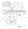
- Fig. 1 is a sectional view of a charge-coupled device of the kind described in the opening paragraph, in which a conventional cl ck voltage is applied to the first clock electrode:
- Fig. 2 shows a diagram of the potential distribution in this device during operation;
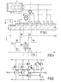
- Fig. 3 shows an embodiment of a semiconductor device according to the invention;
- Fig. 4 shows a diagram of the potential distribution during operation in this device;
- Fig. 5 shows the circuit diagram of a driver circuit used in the device shown in Fig. 3.
- The invention will be described with reference to a surface channel CCD. Although the invention in itself may also be used in charge-coupled devices having a buried channel (BCCD)m for certain applications, for example those in which stringent requirements are imposed on the linearity, charge-coupled devices having a surface channel or BCCD's having an input structure in surface channel technology are often preferred.
- For explanation of the problem to be solved by the invention, Fig. 1 shows a charge-coupled device of the kind described in the opening paragraph, which is controlled with the usual clock voltages. The device, which in this case is of the n-channel type, but may of course also be of the p-channel type, comprises a p-
type semiconductor body 1 of, for example, silicon, at whosesurface 2 thechannel 3 is located. For controlling the charge transport through thechannel 3, thesurface 2 is provided with a row ofclock electrodes 4,5, which are separated by anintermediate oxide layer 6 from the surface. The clock electrodes each comprise a transfer part a and a storage part b, which parts are distinguished from each other by means which are present to induce upon application of a clock voltage below the transfer part a a potential barrier and below the storage part a potential well in thechannel 3. In the present embodiment, these means are constituted by thethicker oxide 6 below thetransfer parts storage parts - However, in other embodiments, this electrode configuration serves to operate the device as a one-bit-per-electrode device, in which all the storage sites but one are filled with information and the vacancy is displaced in the direction opposite to the charge transport direction. Moreover, other electrode configurations, such as one- or three-layer configurations, may also be used.
- The
clock electrodes 4,5 are connected in known manner viaclock lines clock voltage source 9, which supplies the clock voltages 0̸₁,0̸₂ indicated diagrammatically in theblock 9. - The input of the charge-coupled device comprises, viewed in the charge transport direction (from the left to the right), in order of succession: an n⁺ source zone 10 (designated hereinafter as input diode), which supplies electrons for forming the charge packets; a first electrode 11, which constitutes a sample gate, and a
second electrode 12, which constitutes the input gate. - The
input diode 10 is connected to a fixed potential, for example earth. Theinput gate 12 is connected to avoltage source 13, which comprises a signal source and which supplies a signal-dependent voltage to the input electrode 11 determining the size of the charge packet to be formed below theinput electrode 12. The sample electrode 11, which is composed for reasons of manufacturing technology in the same manner as theclock electrodes 4,5 of apart 11a on thicker oxide and apart 11b on thinner oxide, serves as a switch between theinput diode 10 and the storage region below theinput electrode 12. A sample clock 0̸s is applied to the sample gate 11, which clock is supplied by thesource 9. - During operation, the
body 1 is applied to a reference voltage of, for example, -3.5 V, while clock voltages 0̸₁,0̸₂ having levels of 0 and 5 V are applied to the clock electrodes 4.5. The clock 0̸s also varies between 0 and 5 V. Fig. 2 shows the potential distribution occurring at these voltages in a part of the device, the quantity V representing the surface potential which is plotted in downward direction, as is usual for CCD's. In the Figure, the potential levels of the substrate voltage and 5V are also indicated by broken lines. Thelevel 15 represents the potential level of theinput diode 10. The surface potential below the sample gate 11 is indicated byreference numeral 16, the surface a and b designating the potentials below theparts input diode 10 to the region below theinput gate 12 at 0̸s = 5 V, while the flow of electrons is blocked at 0̸s = 0 V. In an analogous manner, the levels 17a,b, 17ʹa,b represent the potentials below thefirst clock electrode input gate 12 corresponding to Vin maximum is determined by thepotential level 15 of theinput diode 10. The lowest effectivepotential level 18 below theinput gate 12 corresponding to the highest input signal Vin is determined by the height of the potential barrier 17a. If, as shown in Fig. 2, Vin exceeds this maximum value, thelevel 18 will fall below the potential level 17a. In this situation, it will no longer be possible to transfer the whole quantity of charge stored below theinput gate 12 to thepotential well 17b below the first clock electrode 4. - In practical embodiments, it has been found that the potential difference between the
levels potential level 12 often lies below the level 17a so that it is not possible to transfer the whole charge packet. - Fig. 3 shows an embodiment of a semiconductor device, in which the problem described above is avoided in a simple manner. For the sake of simplicity, the device is provided for identical parts with the same reference numerals as the device shown in Fig. 1. In contrast with the device shown in Fig. 1, the first clock electrode 4 is now connected not directly, but through the
amplifier 20, to theclock line 7. Preferably, a bootstrap circuit is used for this amplifier so that the supply voltage of 5 V need not be modified. Fig. 5 shows by way of example the circuit diagram of such a circuit. It should be noted that in the circuit diagram transistors of the depletion type are indicated by a double line in the channel region, while transistors of the enhancement type are indicated therein by a single line. The clock signal 0̸₁ supplied by theclock voltage source 9 is supplied to the gate of the transistor T₁, while the amplified output signal 0̸₀ is derived from the drain of the transistor T₅. The circuit comprises two supply lines of 0 V and 5 V. From the lefthand side, the circuit comprises in the first place a first inverter stage comprising the series-combination of a driver transistor T₁ and a load transistor T₂. The first inverter stage is followed by a second similar inverter stage comprising the driver transistor T₃ and the load transistor T₄. The input of this second inverter stage, i.e. the gate of T₃, is connected to theinput 21 of the first inverter stage. The gates of the load transistors T₂ and T₄ are connected to their source zones. The inverter stage T₃,T₄ is followed by a series-combination of three transistors, i.e. T₅, T₆ and T₇. The gate electrodes of the transistors T₅ and T₇ are connected to theoutput 21 of the first inverter stage. The gate of T₆ is connected to theoutput 22 of the second inverter stage T₃,T₄. Thejunction point 23 of T₅ and T₆ is connected to theoutput terminal 24, at which the output signal can be derived, which can be applied to the first clock electrode 4. Thejunction point 25 between the transistors T₆ and T₇ is connected to a plate of the bootstrap capacitance C. On the righthand side of the drawing, a series-combination is shown of two transistors, i.e. the transistor T₈, whose gate is connected to theoutput 21 of the first inverter stage, and the depletion transistor T₉, whose gate is connected to thesource zone 26. The transistor T₁₀ is connected parallel to T₉ and its gate is connected to theoutput 24, i.e. thejunction point 23. Thejunction point 26 between T₈ and T₉ is connected to the second plate of the bootstrap capacitance C. - For explanation of the operation of the circuit, there is started from the situation in which 0̸₁ = 0 V (low). T₁ is non-conducting; the
point 21 then reaches 5 V (high). This signal is inverted again by the inverter stage T₃,T₄ so that thejunction point 22 becomes low (nearly 0 V). In this situation, the transistors T₅ and T₇ are conducting and the transistor T₆ is non-conducting. The junction point 23 (also consituting the output) is applied to 0 V and thejunction point 25 is applied to 5 V. At the same time, be cause T₈ is conducting and T₁₀ is non-conducting, thejunction point 26 is applied to (nearly) 0 V. If now 0̸₁ passes to 5 V (high), the junction points 21 and 22 pass to 0 V and 5 V, respectively. The transistors T₅ and T₇ are then non-conducting and T₆ becomes conducting. At the same time, T₈ becomes non-conducting, as a result of which the voltage at thejunction point 26 increases to 5 V. Due to the fact that the bootstrap capacitance C is connected to thejunction point 26 and the transistors T₅ and T₇ are non-conducting, the voltage at thejunction point 25 which was already applied to 5 V, to a value of practically 10 V. Due to capacitive voltage divisions, the ultimate potential value at thepoint 25 may be slightly lower than 10 V. Since in this situation the transistor T₆ is conducting, thejunction point 23 and hence theoutput 24 follows the voltage source of thejunction point 25 to nearly 10 V. The transistor T₁₀, which in this situation is also conducting, only serves to increase the speed at which thejunction point 26 is charged. - By the use of the bootstrap driver circuit shown in Fig. 5, it is possible to obtain, whilst using 5 V clock voltages 0̸₁,0̸₂, a transfer of the whole charge packet below the input gate to the first clock electrode 4, as is shown in Fig. 4. In this Figure, for corresponding potential levels the same reference numerals as in Fig. 2 are used. The difference between Fig. 4 and Fig. 2 mainly resides in the fact that at 0̸₁ = 5 V the potential level 17ʺa, 17ʺb lies now a few volts lower than the
level 17a, 17b in Fig. 2. As a result, also if Vin is a maximum, thelevel 18 will lie above the potential level 17ʺa so that the whole quantity of charge stored at this value of Vin below theinput gate 12 can flow to thecharge transport channel 3. The signal distortion described in the preamble that may occur in conventional devices due to incomplete charge transport is avoided in a simple manner in the device described here according to the invention without it being necessary to reduce the input signal Vin. Moreover, in the device des cribed here, the remaining clock electrodes can be driven by means of conventional low clock voltage 0̸₁,0̸₂ of 0 and 5 V so that the dissipation substantially does not increase. - It will be appreciated that the invention is not limited to the embodiment shown, but that many variations are possible for those skilled in the art without departing from the scope of the invention. For example, the invention may be used not only in charge-coupled devices with incorporated potential barriers, but also in devices in which this barrier is not present, such as, for example, in the four-phase device described in the aforementioned publication.
Claims (5)
Applications Claiming Priority (2)
| Application Number | Priority Date | Filing Date | Title |
|---|---|---|---|
| NL8600891 | 1986-04-09 | ||
| NL8600891A NL8600891A (en) | 1986-04-09 | 1986-04-09 | SEMICONDUCTOR DEVICE. |
Publications (2)
| Publication Number | Publication Date |
|---|---|
| EP0244889A1 true EP0244889A1 (en) | 1987-11-11 |
| EP0244889B1 EP0244889B1 (en) | 1990-10-24 |
Family
ID=19847850
Family Applications (1)
| Application Number | Title | Priority Date | Filing Date |
|---|---|---|---|
| EP87200594A Expired - Lifetime EP0244889B1 (en) | 1986-04-09 | 1987-03-31 | Ccd input circuit |
Country Status (10)
| Country | Link |
|---|---|
| US (1) | US4774719A (en) |
| EP (1) | EP0244889B1 (en) |
| JP (1) | JPH0724307B2 (en) |
| KR (1) | KR950004868B1 (en) |
| CN (1) | CN1005939B (en) |
| AT (1) | ATE57786T1 (en) |
| AU (1) | AU592171B2 (en) |
| CA (1) | CA1291567C (en) |
| DE (1) | DE3765687D1 (en) |
| NL (1) | NL8600891A (en) |
Families Citing this family (5)
| Publication number | Priority date | Publication date | Assignee | Title |
|---|---|---|---|---|
| JPH0728029B2 (en) * | 1987-05-21 | 1995-03-29 | 株式会社東芝 | Charge transfer device |
| NL8800851A (en) * | 1988-04-05 | 1989-11-01 | Philips Nv | SEMICONDUCTOR MEMORY DEVICE. |
| US6573541B1 (en) | 2000-09-29 | 2003-06-03 | International Business Machines Corporation | Charge coupled device with channel well |
| US7046283B1 (en) | 2000-10-11 | 2006-05-16 | Dalsa, Inc. | Arrangements of clock line drivers |
| JP4249433B2 (en) * | 2002-05-15 | 2009-04-02 | Necエレクトロニクス株式会社 | Charge transfer device and manufacturing method thereof |
Family Cites Families (2)
| Publication number | Priority date | Publication date | Assignee | Title |
|---|---|---|---|---|
| US3925805A (en) * | 1974-01-28 | 1975-12-09 | Hughes Aircraft Co | System for transferring charge between spaced apart CCDs by direct series connection |
| NL8600890A (en) * | 1986-04-09 | 1987-11-02 | Philips Nv | SEMICONDUCTOR DEVICE. |
-
1986
- 1986-04-09 NL NL8600891A patent/NL8600891A/en not_active Application Discontinuation
-
1987
- 1987-03-31 AT AT87200594T patent/ATE57786T1/en active
- 1987-03-31 DE DE8787200594T patent/DE3765687D1/en not_active Expired - Lifetime
- 1987-03-31 US US07/033,129 patent/US4774719A/en not_active Expired - Fee Related
- 1987-03-31 EP EP87200594A patent/EP0244889B1/en not_active Expired - Lifetime
- 1987-04-02 CA CA000533696A patent/CA1291567C/en not_active Expired - Lifetime
- 1987-04-04 CN CN87102618.XA patent/CN1005939B/en not_active Expired
- 1987-04-06 KR KR1019870003241A patent/KR950004868B1/en active IP Right Grant
- 1987-04-08 AU AU71189/87A patent/AU592171B2/en not_active Ceased
- 1987-04-08 JP JP62084883A patent/JPH0724307B2/en not_active Expired - Lifetime
Non-Patent Citations (1)
| Title |
|---|
| INTERNATIONAL CONFERENCE ON TECHNOLOGY AND APPLICATIONS OF CHARGE COUPLED DEVICES, September 1974, pages 13-21, Edinburg, GB; H. WALLINGA: "A comparison of CCD analog input circuit characteristics" * |
Also Published As
| Publication number | Publication date |
|---|---|
| AU7118987A (en) | 1987-10-15 |
| EP0244889B1 (en) | 1990-10-24 |
| CN87102618A (en) | 1987-10-21 |
| NL8600891A (en) | 1987-11-02 |
| CA1291567C (en) | 1991-10-29 |
| KR950004868B1 (en) | 1995-05-15 |
| US4774719A (en) | 1988-09-27 |
| DE3765687D1 (en) | 1990-11-29 |
| JPS62243365A (en) | 1987-10-23 |
| KR870010633A (en) | 1987-11-30 |
| JPH0724307B2 (en) | 1995-03-15 |
| AU592171B2 (en) | 1990-01-04 |
| CN1005939B (en) | 1989-11-29 |
| ATE57786T1 (en) | 1990-11-15 |
Similar Documents
| Publication | Publication Date | Title |
|---|---|---|
| US4130890A (en) | Integrated DDC memory with bitwise erase | |
| JPS62120121A (en) | Cmos output driving circuit | |
| US4084108A (en) | Integrated circuit device | |
| US4037243A (en) | Semi conductor memory cell utilizing sensing of variations in PN junction current conrolled by stored data | |
| US4417162A (en) | Tri-state logic buffer circuit | |
| EP0244889A1 (en) | CCD input circuit | |
| EP0281113B1 (en) | Semi-conductor buffer circuit | |
| EP0133721A1 (en) | Semiconductor device | |
| US4771445A (en) | Charge-coupled device having an improved input stage | |
| US4661726A (en) | Utilizing a depletion mode FET operating in the triode region and a depletion mode FET operating in the saturation region | |
| JP4085512B2 (en) | High side switch circuit | |
| US4280067A (en) | Semiconductor charge transfer device having a decoupling gate for stopping reverse charge flow | |
| CA1101994A (en) | Linear ccd input circuit | |
| US4503550A (en) | Dynamic CCD input source pulse generating circuit | |
| US5422592A (en) | Input circuit of semiconductor integrated circuit device | |
| US5821588A (en) | Transistor and semiconductor device | |
| EP0013117B1 (en) | A mos dynamic logic circuit | |
| EP0205221B1 (en) | Charge-coupled device | |
| EP0132536A1 (en) | Transistor driver circuit | |
| GB1579032A (en) | Low noise ccd input circuit | |
| JPS6222459B2 (en) | ||
| JPS6142359B2 (en) | ||
| US6069826A (en) | Method of rewriting in nonvolatile semiconductor memory device | |
| US4707844A (en) | Integrated circuit having reduced clock cross-talk | |
| EP0114476A2 (en) | Improvements in or relating to driver circuits |
Legal Events
| Date | Code | Title | Description |
|---|---|---|---|
| PUAI | Public reference made under article 153(3) epc to a published international application that has entered the european phase |
Free format text: ORIGINAL CODE: 0009012 |
|
| 17P | Request for examination filed |
Effective date: 19870331 |
|
| AK | Designated contracting states |
Kind code of ref document: A1 Designated state(s): AT BE CH DE FR GB IT LI NL SE |
|
| D17P | Request for examination filed (deleted) | ||
| R17P | Request for examination filed (corrected) |
Effective date: 19880502 |
|
| 17Q | First examination report despatched |
Effective date: 19891124 |
|
| GRAA | (expected) grant |
Free format text: ORIGINAL CODE: 0009210 |
|
| AK | Designated contracting states |
Kind code of ref document: B1 Designated state(s): AT BE CH DE FR GB IT LI NL SE |
|
| PG25 | Lapsed in a contracting state [announced via postgrant information from national office to epo] |
Ref country code: NL Effective date: 19901024 Ref country code: BE Effective date: 19901024 |
|
| REF | Corresponds to: |
Ref document number: 57786 Country of ref document: AT Date of ref document: 19901115 Kind code of ref document: T |
|
| REF | Corresponds to: |
Ref document number: 3765687 Country of ref document: DE Date of ref document: 19901129 |
|
| ITF | It: translation for a ep patent filed |
Owner name: ING. C. GREGORJ S.P.A. |
|
| ET | Fr: translation filed | ||
| NLV1 | Nl: lapsed or annulled due to failure to fulfill the requirements of art. 29p and 29m of the patents act | ||
| PG25 | Lapsed in a contracting state [announced via postgrant information from national office to epo] |
Ref country code: LI Effective date: 19910331 Ref country code: CH Effective date: 19910331 Ref country code: AT Effective date: 19910331 |
|
| PG25 | Lapsed in a contracting state [announced via postgrant information from national office to epo] |
Ref country code: SE Effective date: 19910401 |
|
| PLBE | No opposition filed within time limit |
Free format text: ORIGINAL CODE: 0009261 |
|
| STAA | Information on the status of an ep patent application or granted ep patent |
Free format text: STATUS: NO OPPOSITION FILED WITHIN TIME LIMIT |
|
| 26N | No opposition filed | ||
| REG | Reference to a national code |
Ref country code: CH Ref legal event code: PL |
|
| PGFP | Annual fee paid to national office [announced via postgrant information from national office to epo] |
Ref country code: GB Payment date: 19940301 Year of fee payment: 8 |
|
| PGFP | Annual fee paid to national office [announced via postgrant information from national office to epo] |
Ref country code: FR Payment date: 19940330 Year of fee payment: 8 |
|
| ITTA | It: last paid annual fee | ||
| PGFP | Annual fee paid to national office [announced via postgrant information from national office to epo] |
Ref country code: DE Payment date: 19940527 Year of fee payment: 8 |
|
| EUG | Se: european patent has lapsed |
Ref document number: 87200594.7 Effective date: 19911108 |
|
| PG25 | Lapsed in a contracting state [announced via postgrant information from national office to epo] |
Ref country code: GB Effective date: 19950331 |
|
| ITPR | It: changes in ownership of a european patent |
Owner name: CAMBIO RAGIONE SOCIALE;PHILIPS ELECTRONICS N.V. |
|
| GBPC | Gb: european patent ceased through non-payment of renewal fee |
Effective date: 19950331 |
|
| PG25 | Lapsed in a contracting state [announced via postgrant information from national office to epo] |
Ref country code: FR Free format text: LAPSE BECAUSE OF NON-PAYMENT OF DUE FEES Effective date: 19951130 |
|
| PG25 | Lapsed in a contracting state [announced via postgrant information from national office to epo] |
Ref country code: DE Effective date: 19951201 |
|
| REG | Reference to a national code |
Ref country code: FR Ref legal event code: ST |
|
| PG25 | Lapsed in a contracting state [announced via postgrant information from national office to epo] |
Ref country code: IT Free format text: LAPSE BECAUSE OF NON-PAYMENT OF DUE FEES Effective date: 20050331 |