EP0244634A2 - Atténuateur variable - Google Patents
Atténuateur variable Download PDFInfo
- Publication number
- EP0244634A2 EP0244634A2 EP87104846A EP87104846A EP0244634A2 EP 0244634 A2 EP0244634 A2 EP 0244634A2 EP 87104846 A EP87104846 A EP 87104846A EP 87104846 A EP87104846 A EP 87104846A EP 0244634 A2 EP0244634 A2 EP 0244634A2
- Authority
- EP
- European Patent Office
- Prior art keywords
- resistance
- sliding contacts
- attenuator according
- rotating body
- drum
- Prior art date
- Legal status (The legal status is an assumption and is not a legal conclusion. Google has not performed a legal analysis and makes no representation as to the accuracy of the status listed.)
- Granted
Links
- 238000000576 coating method Methods 0.000 claims abstract description 23
- 239000011248 coating agent Substances 0.000 claims abstract description 19
- 230000002093 peripheral effect Effects 0.000 claims description 7
- 239000000969 carrier Substances 0.000 claims description 6
- 230000001419 dependent effect Effects 0.000 claims description 5
- 238000005516 engineering process Methods 0.000 claims description 3
- 239000002184 metal Substances 0.000 description 9
- 238000013016 damping Methods 0.000 description 8
- 230000005540 biological transmission Effects 0.000 description 5
- 238000010586 diagram Methods 0.000 description 5
- 239000000463 material Substances 0.000 description 4
- 238000004519 manufacturing process Methods 0.000 description 2
- 238000000034 method Methods 0.000 description 2
- 229910000679 solder Inorganic materials 0.000 description 2
- 238000005476 soldering Methods 0.000 description 2
- 229910010293 ceramic material Inorganic materials 0.000 description 1
- 239000004020 conductor Substances 0.000 description 1
- 239000012777 electrically insulating material Substances 0.000 description 1
- 238000009713 electroplating Methods 0.000 description 1
- 239000011810 insulating material Substances 0.000 description 1
- 238000010422 painting Methods 0.000 description 1
- 238000007639 printing Methods 0.000 description 1
- 230000000284 resting effect Effects 0.000 description 1
- 210000002105 tongue Anatomy 0.000 description 1
Images


Classifications
-
- H—ELECTRICITY
- H03—ELECTRONIC CIRCUITRY
- H03H—IMPEDANCE NETWORKS, e.g. RESONANT CIRCUITS; RESONATORS
- H03H7/00—Multiple-port networks comprising only passive electrical elements as network components
- H03H7/24—Frequency- independent attenuators
Definitions
- the invention relates to an adjustable attenuator with at least two simultaneously adjustable ohmic resistors, each of which lies from a resistance section between two sliding contacts of constant length, and in which the sliding contacts rest on a rotating body that is mechanically rotatable relative to the sliding contacts and one in the grinding area Has resistance coating.
- Attenuators are used to extract part of the wave energy of electromagnetic waves on lines in the high frequency range. These are changeable voltage dividers with a defined real input and output resistance. They consist of resistors in symmetrical or unsymmetrical, T - or bridged T-circuit. Attenuators are known which contain current sources (electron tubes, transistors, PIN diodes), that is to say active four poles. The subject of the innovation, however, is a passive four-pole system that contains no current sources. It should have a predetermined wave resistance and be used for damping at wave frequencies from 0 to the gigahertz range, with the transmission loss a d being continuously adjustable between a start and end value.
- Passive attenuators are known which produce high return loss a r , a four-pole in symmetrical T or Circuit of three sheet resistors is present. This means that only a defined through loss is achieved. If different damping should be adjustable, it must be switched between several resistors. The transmission loss a d is therefore not continuous, but can only be adjusted step by step.
- Continuously variable attenuators have resistors which are designed as three layer resistance elements arranged in parallel at a distance, on which a sliding contact with three pickups can be moved via a spindle.
- Attenuators of the type mentioned which are characterized in that the resistance coating is formed from a coating which is applied to at least one surface of the rotating body and correspondingly one between.
- Rotating bodies are to be understood in particular as drums, disks or disk arrangements, at least one of the following areas being provided with a resistance coating: the end faces, the inner lateral surface, the outer lateral surface, the periphery.
- Rotating bodies are to be understood as meaning all suitable bodies on which sliding contacts can rest in the manner described while the rotating body is being rotated. Usually these are the drums or disk arrangements already mentioned. However, structures are also conceivable that can be represented as cutouts (segments) of the above elements. In addition, polygonal prisms, cylinders with ellipsoidal floor plans and the like could also be thought of.
- Essential to the invention in the attenuator according to the invention is that there are verifiable surfaces.
- a hollow drum or a hollow cylinder is selected.
- One, two or more of these surfaces are each covered by a suitable, preferably equally wide, resistance layer or a resistance covering.
- a drum instead of a drum also can contact Scheibenanordnun g, arranged in between the drum can or lamellar, parallel discs provided air or some other dielectric is present.
- the transmission loss can either be set continuously or in steps between a start and end value.
- a rotating body suitable for the damping member consists of an electrically insulating material, for example ceramic material, on the carrier surface of which the resistance layers are applied by printing, painting, electroplating and similar techniques known per se.
- the resistance techniques are graphite- or metal-containing layers or other “exotic” plastic materials, as they are known per se or can be developed in an adapted manner. It is also possible to first apply a relatively thick layer of material and to remove it more or less according to the desired resistance dependence on the angle of rotation1. The layers can be changed continuously; However, it is also possible to create a quasi-continuity by placing a large number of resistance layers, up to a quasi-infinitesimal number, of resistance layers next to one another in the manner of rays or lines.
- a resistance coating may be applied a adiuscardi equal width in R segment of a circle on an end face of the drum or disc in shape, with the ohmic resistance is dependent on the angle of rotation lying on the resistance path in the radius direction.
- the drum carries at least one strip-shaped resistance covering on its outer or inner casing, on which or on which two sliding contacts lie at constant peripheral or epipheral or axial spacing, the resistance covering also being such that the ohmic resistance per unit distance in peripheral, epipheral or axial distance depends on the angle of rotation ⁇ .
- Resistance coverings can also be applied in such a way that they are attached to a common surface and contact one another in the edge area.
- the sliding contacts can be attached to the ends of flags or contact pins. It is also possible that, in the presence of a waveguide using stripline technology, the sliding contacts are attached to the ends of such waveguides.
- the attenuator is preferably enclosed in a housing.
- the drum z. B. is connected to a ring gear in which a rotating spindle provided with a worm gear engages, so that an exact rotary movement is possible.
- the carrier body of the sliding contacts can be introduced and held in the housing, which is preferably made of plastic. It is also possible to provide the housing walls with openings so that one or both stub axles of the drum are rotatably held in the openings.
- the housing can be provided with a metallic conductive surface.
- the values for the ohmic resistances coming to the attenuator are largely variable according to the task, size of the attenuator, short-circuit strength and similar conditions.
- a typical example uses a resistance layer on the front side, in which the resistance values vary between approx. 10 and 40 kOhm; the resistance values on the outer surfaces vary between approx. 10 mOhm and 600 Ohm, according to the required wave resistance and the maximum transmission loss.
- An advantage of all the above-mentioned and still to be described embodiments is that the direction of propagation of the electromagnetic wave on the resistance layers between the sliding contacts runs both parallel and perpendicular to the direction of movement of the carrier head, and the damping takes place accordingly.
- the path length of the electromagnetic wave on the resistance surface of the Carrier body is minimal and constant for all positions of the carrier body.
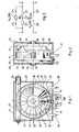
- FIG. 1 and 2 show an attenuator in a first embodiment.
- the attenuator is enclosed in a housing 11, which has the shape of a cuboid on the outside. Typical dimensions of this cuboid are 30 x 30 x 15 mm. These dimensions are only for explanation and are not to be understood as restrictive.
- the front and rear walls 12 and 13 of the housing 11 are provided with opposite bores 14, 15 in which Axle stub 16, 17 of a drum 18 made of insulating material are rotatably embedded.
- One of the stub axles (17) is provided with a slot 19 so that a torque can be exerted on the axis of the drum 18.
- the drum 18 has a substantially cylindrical shape.
- a toothed ring 20 On its side facing the front wall 12, it is provided with a toothed ring 20, into which a rotating spindle 21 provided with a worm gear engages.
- the rotary spindle 21 is also mounted in two housing walls 22, 23. It protrudes from the housing with an adjusting pin 24 and is provided with a slot so that a torque can be exerted on it.
- This resistance coating 26 is such that in the radius direction A the ohmic resistance of a resistance path 26 'between two contacts lying on the resistance coating is different at different positions of the drum, depending on the angle of rotation? is. Based on the special embodiment according to FIG. 1, the greatest resistance is accordingly at the beginning of the resistance layer (at 27) and the smallest at the end of the resistance layer (at 28).
- sliding contacts 29 and 30 are arranged in the area of the inner and outer edge of the resistance covering 26, making contact with it.
- the sliding contact 30 is also anchored in the housing via a contact carrier 36. The resistance distance between the two sliding contacts 29, 30 is therefore exactly in the radial direction and always has the same length.
- a further resistance covering 39 is applied to the outer casing 38 of the drum 18, specifically in the form of an outer casing which is interrupted at 40.
- the resistance coating 39 consists of a resting, equally wide strip which is such that the ohmic resistance per unit distance in peripheral A b-stand is continuously variable, depending on the rotation angle ff. This results in different resistances along the periphery.
- the resistors are tapped by two sliding contacts 41, 42, which in turn are fixed at the end to corresponding contact carriers 43, 44.
- the sliding contacts touch the outside of the resistance covering 39, possibly in a staggered arrangement, as can be seen from FIGS. 1 and 2.
- the resistance path 39 'between the two contacts 41 and 42 is always the same length regardless of the position of the drum.
- the contact carriers 43, 44 are each connected to the contact carrier 36 via a sheet resistor 37, 37 '.
- connection points are designated 1, 2, 1 ', 2', 30. These points can be found again in the equivalent circuit diagram according to FIG. 3. It can be seen that the resistor R 1 is assigned to the resistance section 39 ', while the resistor R 2 is assigned to the resistance section 26'. From the consideration of the mechanical parts according to Figures 1 and 2 and the equivalent circuit diagram according to Figure 3 it can be seen that the resistors R 1 and R 2 can be adjusted in the same direction or in opposite directions if the Resistance pads 26 or 39 increase proportionally or inversely proportional in the resistance with the angle of rotation.
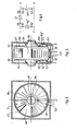
- FIGS. 4 and 5 A further embodiment of an attenuator is shown in FIGS. 4 and 5.
- the drum 18 is designed for a ⁇ circuit.
- the outer jacket of the drum 18 carries a resistance covering 47 in the form of a strip which covers most of the circumference but has a gap 46.
- the resistance coating 47 is contacted in the lower region of the housing 11 by two sliding contacts 48, 49, between which a defined resistance path 47 'is produced in the axial direction.
- resistance coverings 54, 55 in the form of a circle segment of equal width in the radius direction are applied to both end faces 50, 51, with sliding contacts 52, 52' and 53, 53 'each in the area of the inner and outer edge of the resistance coverings Contact 54 or 55.
- the resistance linings 54 and 55 are also such that the ohmic resistance in the radius direction is proportional to the angle of rotation ⁇ at various positions of the drum. The resistance between the sliding contacts 52-52 'and 53-53' can therefore be changed continuously and continuously without changing the length of the resistance path 54 'or 55'.
- FIG. 6 shows an equivalent circuit diagram for the attenuator according to FIGS. 4 and 5.
- the corresponding contacts and positions are identified by the same numbers.
- the sliding contacts 52, 52 'and 53, 53' are connected in a similar manner to contact carriers which end in solder lugs, as has also been described with reference to FIGS. 1 and 2.
- the drum 18 is adjusted through a slot which has been let into a stub shaft 56.
- FIGS. 7 and 8 show a further possibility for implementing an attenuator.
- a W is iderstandsbelag 57 applied in mecanical hollow drum 18 '.
- Two sliding contacts 58, 59 are located in the edge region of this resistance covering 57.
- a resistance path 57 1 is located between the sliding contacts 58, 59.
- the drum 18 ' is rotatable by a worm spindle 60 which rotates within a ring gear 62 embedded in an annular groove 61 and thus drives the drum 18'.
- two further resistance coatings 63, 64 are applied in two electrically separated strips, which are contacted by corresponding sliding contacts 65, 66.
- further sliding contacts 65 '(another is covered) are at an angular distance from one another, so that, with the appropriate properties of the resistance coatings, a continuously variable resistance can be produced with the same resistance distance between the sliding contacts.
- the distance between the sliding contacts on the outside (peripheral) or inside in the sheath (epipher) of the resistance layers is approximately between 10 and 45 °. A compromise must be found between the accuracy of the resistance and the width of the variation, the choice also depending on the size of the rotating body and damping element as a whole.
- the resistance values between the sliding contacts vary according to the needs and conditions for such dampers circuitry. Suitable values have already been discussed in the introduction to the description.
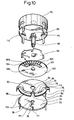
- FIGS. 9 to 11 A further embodiment is shown in FIGS. 9 to 11, which has proven to be particularly suitable in practice.
- the parts which are drawn in an exploded view in FIG. 10 are located in a cylindrical housing 70 according to FIG.
- the housing 70 consists of plastic, which is metallized on its surface, or of a metal sheet.
- the housing 70 is provided in its cover 71 with a circular axis passage 72.
- notches 73 are provided, from which tongues 74 of a base part 75 to be described protrude.
- a base 76 inserted into the housing 70 can be seen in FIG. 10, which consists of two layers: a non-conductive plastic material and an overlying metal layer 76 '. However, it is also possible to produce the floor entirely from sheet metal.
- the bottom 76 is fitted into the housing 70, for example welded or glued.
- a contact tab 77 is fixedly placed on the bottom 76 to establish an electrical connection with the metal layer 76 '.
- the contact tab 77 is bent upward to form a sliding contact 78.
- a second, identical contact tab 77 ' can be placed on the bottom 76 in a conductive manner. This contact lug is offset both radially and tangentially to the contact lug 77, specifically towards the center of the floor.
- the center of the bottom 76 is occupied by a circular opening 79 which lies opposite the axis passage 72 of the housing 70.
- Two soldering swords 112 are connected to the metal layer 76 ′ as ground contacts on the bottom 76.
- the base part 75 which consists of a plastic plate which has a continuous metal layer 80 on its underside.
- Two soldering swords 113 are connected to the metal layer 80 as a ground contact. Insulated from this metal layer 80, two metallic, strip-shaped waveguides 91, 92 are provided on the upper side, which have an approximately crescent shape, are symmetrical to one another and each end at an edge of a slot 93 provided in the base part 75.
- the waveguides 91, 92 serve as carriers for two sliding contacts 95, 96. Furthermore, a central opening 94 is provided in the base part 75 as a passage. A flanged, contoured stub axle 98 is held in the openings 79, 94 and 72 and has a slot 99 on its upper side, via which a torque can be exerted on the stub axle 98 by means of a screwdriver.
- the stub shaft 98 carries a rotating body 100, which is designed as a flat circular disc and consists essentially of insulating plastic.
- the rotating body 100 is shown in FIG. 11 seen from below.
- the rotating body 100 is touched on its underside shown in FIG. 11 by the two sliding contacts 95, 96 and by the sliding contact 78. These points of contact are designated with points and a corresponding numbering in FIG. 11.
- the rotating body 100 is provided with a central bore 108, wherein the rotation can be effected by means of a stub shaft 98 via a corresponding contour.
- a spring washer 110 is also installed in order to stabilize the installed system.
- Another abutment is formed by the shoulders 114 projecting inwards on the housing.
- the rotating body 100 carries on its underside two contacting segment-like resistance coatings 101 and 102.
- the resistance coating 101 consists of a continuous layer which, however, has a continuously increasing resistance coefficient in the tangential direction T.
- the resistance path 103 located between the two contacts 95 and 96 accordingly has a different value depending on the position of the rotating body 100. In the area of the resistance coating 102, this arrangement is chosen differently. Here individual resistance paths in the form of parallel strips 104 are applied, between which non-conductive zones 105 lie.
- the non-conductive zones 105 are considerably narrower than the strips 104; the former are made from a continuous covering z. B. burned out by laser beams.
- Each strip 104 measured from start to finish, has a higher or lower value than its neighboring strip. Accordingly, the resistance that exists between the contact 78 and the contact area 106 between the two resistance linings 101 and 102 differs depending on the position of the rotating body 100. Accordingly, the two resistance zones 101 and 102 are in contact with one another in the regions in which the strips 104 touch the resistance strip 101.
- a T circuit can be achieved in a simple manner with the aid of the attenuator shown in FIGS. 9-11.
- 17 circuits can also be implemented.
- a particular advantage is that the sliding contacts 95, 96 are located at the ends of two waveguides that have been attached using stripline technology. In this way, the production of attenuators, in which waveguides are contained, can be substantially rationalized.
- FIG. 12 finally shows one possible embodiment of the rotating body, reference number 100 ', in which three segment-like resistance coverings 101', 102 'and 115 which come into contact with one another lie next to one another in the form of circular segments.
Landscapes
- Adjustable Resistors (AREA)
- Liquid Crystal Substances (AREA)
- Surface Acoustic Wave Elements And Circuit Networks Thereof (AREA)
- Oscillators With Electromechanical Resonators (AREA)
Applications Claiming Priority (2)
| Application Number | Priority Date | Filing Date | Title |
|---|---|---|---|
| DE8609032U | 1986-04-04 | ||
| DE8609032U DE8609032U1 (de) | 1986-04-04 | 1986-04-04 | Verstellbares Dämpfungsglied |
Publications (3)
| Publication Number | Publication Date |
|---|---|
| EP0244634A2 true EP0244634A2 (fr) | 1987-11-11 |
| EP0244634A3 EP0244634A3 (en) | 1989-07-12 |
| EP0244634B1 EP0244634B1 (fr) | 1995-07-26 |
Family
ID=6793298
Family Applications (1)
| Application Number | Title | Priority Date | Filing Date |
|---|---|---|---|
| EP87104846A Expired - Lifetime EP0244634B1 (fr) | 1986-04-04 | 1987-04-02 | Atténuateur variable |
Country Status (3)
| Country | Link |
|---|---|
| EP (1) | EP0244634B1 (fr) |
| AT (1) | ATE125656T1 (fr) |
| DE (2) | DE8609032U1 (fr) |
Citations (2)
| Publication number | Priority date | Publication date | Assignee | Title |
|---|---|---|---|---|
| GB886488A (en) | 1957-05-20 | 1962-01-10 | Plessey Co Ltd | Improvements in and relating to variable resistors and potentiometers |
| FR2111961A1 (fr) | 1970-10-30 | 1972-06-09 | Tektronix Inc |
-
1986
- 1986-04-04 DE DE8609032U patent/DE8609032U1/de not_active Expired
-
1987
- 1987-04-02 DE DE3751425T patent/DE3751425D1/de not_active Expired - Fee Related
- 1987-04-02 AT AT87104846T patent/ATE125656T1/de not_active IP Right Cessation
- 1987-04-02 EP EP87104846A patent/EP0244634B1/fr not_active Expired - Lifetime
Patent Citations (2)
| Publication number | Priority date | Publication date | Assignee | Title |
|---|---|---|---|---|
| GB886488A (en) | 1957-05-20 | 1962-01-10 | Plessey Co Ltd | Improvements in and relating to variable resistors and potentiometers |
| FR2111961A1 (fr) | 1970-10-30 | 1972-06-09 | Tektronix Inc |
Also Published As
| Publication number | Publication date |
|---|---|
| DE3751425D1 (de) | 1995-08-31 |
| DE8609032U1 (de) | 1987-03-05 |
| ATE125656T1 (de) | 1995-08-15 |
| EP0244634B1 (fr) | 1995-07-26 |
| EP0244634A3 (en) | 1989-07-12 |
Similar Documents
| Publication | Publication Date | Title |
|---|---|---|
| DE2513498C3 (de) | Koaxiale Zwischenkupplung für Antennen-Koaxialkabel | |
| DE2615996C2 (de) | Einstückig aus Metallblech gestanzte und geformte elektrische Anschlußklemme | |
| CH638926A5 (de) | Vakuumschalter mit magnetspule. | |
| DE4414529A1 (de) | Drehwinkelsensor vom Kapazitätstyp | |
| DE3215323C2 (fr) | ||
| DE2229315C3 (de) | Trimmerkondensator | |
| DE1766903B1 (de) | Streifenleitungszirkulator | |
| DE2940583A1 (de) | Variable widerstandssteuereinrichtung | |
| DE2048528A1 (de) | Mikrowellenvorrichtung | |
| DE1463269C3 (de) | Vorionisator zur Verwendung in einem Überspannungsableiter | |
| DE1944960C3 (de) | Filtereinrichtung | |
| EP0244634B1 (fr) | Atténuateur variable | |
| DE2908255C2 (de) | Y-Zirkulator | |
| DE2931855C2 (fr) | ||
| DE68925117T2 (de) | Insbesondere für temperaturmessung gedachter thermistor und verfahren zur herstellung | |
| DE1246060B (de) | Hochfrequenzschalter | |
| DE2246573C3 (de) | Abgleichbarer Schichtkondensator | |
| DE3136471C2 (de) | Drehschalter | |
| DE917615C (de) | Koaxiale Hochfrequenzleitung, deren Innenleiter in der Mitte des Aussenleiters durch Distanzscheiben gelagert ist | |
| DE1813153A1 (de) | Vorrichtung zur Umformung einer mechanischen Wegaenderung in elektrische Signale | |
| DE1791108B1 (de) | Mehrarmiger zirkulator | |
| EP0187951A1 (fr) | Contact interrupteur pour un interrupteur sous vide | |
| EP0896381B1 (fr) | Composant à micro-ondes | |
| DE2453851A1 (de) | Hochfrequenz-phasenschieber in gedruckter technik | |
| DE2741553A1 (de) | Veraenderbares, elektrisches bauelement |
Legal Events
| Date | Code | Title | Description |
|---|---|---|---|
| PUAI | Public reference made under article 153(3) epc to a published international application that has entered the european phase |
Free format text: ORIGINAL CODE: 0009012 |
|
| AK | Designated contracting states |
Kind code of ref document: A2 Designated state(s): AT BE CH DE ES FR GB IT LI NL SE |
|
| PUAL | Search report despatched |
Free format text: ORIGINAL CODE: 0009013 |
|
| AK | Designated contracting states |
Kind code of ref document: A3 Designated state(s): AT BE CH DE ES FR GB IT LI NL SE |
|
| 17P | Request for examination filed |
Effective date: 19891118 |
|
| 17Q | First examination report despatched |
Effective date: 19920324 |
|
| GRAA | (expected) grant |
Free format text: ORIGINAL CODE: 0009210 |
|
| AK | Designated contracting states |
Kind code of ref document: B1 Designated state(s): AT BE CH DE ES FR GB IT LI NL SE |
|
| PG25 | Lapsed in a contracting state [announced via postgrant information from national office to epo] |
Ref country code: IT Free format text: LAPSE BECAUSE OF FAILURE TO SUBMIT A TRANSLATION OF THE DESCRIPTION OR TO PAY THE FEE WITHIN THE PRE;WARNING: LAPSES OF ITALIAN PATENTS WITH EFFECTIVE DATE BEFORE 2007 MAY HAVE OCCURRED AT ANY TIME BEFORE 2007. THE CORRECT EFFECTIVE DATE MAY BE DIFFERENT FROM THE ONE RECORDED.SCRIBED TIME-LIMIT Effective date: 19950726 Ref country code: FR Effective date: 19950726 Ref country code: BE Effective date: 19950726 Ref country code: GB Effective date: 19950726 Ref country code: NL Free format text: LAPSE BECAUSE OF FAILURE TO SUBMIT A TRANSLATION OF THE DESCRIPTION OR TO PAY THE FEE WITHIN THE PRESCRIBED TIME-LIMIT Effective date: 19950726 |
|
| REF | Corresponds to: |
Ref document number: 125656 Country of ref document: AT Date of ref document: 19950815 Kind code of ref document: T |
|
| REF | Corresponds to: |
Ref document number: 3751425 Country of ref document: DE Date of ref document: 19950831 |
|
| PG25 | Lapsed in a contracting state [announced via postgrant information from national office to epo] |
Ref country code: SE Effective date: 19951026 |
|
| PG25 | Lapsed in a contracting state [announced via postgrant information from national office to epo] |
Ref country code: ES Free format text: LAPSE BECAUSE OF FAILURE TO SUBMIT A TRANSLATION OF THE DESCRIPTION OR TO PAY THE FEE WITHIN THE PRESCRIBED TIME-LIMIT Effective date: 19951106 |
|
| EN | Fr: translation not filed | ||
| NLV1 | Nl: lapsed or annulled due to failure to fulfill the requirements of art. 29p and 29m of the patents act | ||
| GBV | Gb: ep patent (uk) treated as always having been void in accordance with gb section 77(7)/1977 [no translation filed] |
Effective date: 19950726 |
|
| PG25 | Lapsed in a contracting state [announced via postgrant information from national office to epo] |
Ref country code: AT Effective date: 19960402 |
|
| PG25 | Lapsed in a contracting state [announced via postgrant information from national office to epo] |
Ref country code: LI Effective date: 19960430 Ref country code: CH Effective date: 19960430 |
|
| PLBE | No opposition filed within time limit |
Free format text: ORIGINAL CODE: 0009261 |
|
| STAA | Information on the status of an ep patent application or granted ep patent |
Free format text: STATUS: NO OPPOSITION FILED WITHIN TIME LIMIT |
|
| 26N | No opposition filed | ||
| REG | Reference to a national code |
Ref country code: CH Ref legal event code: PL |
|
| PG25 | Lapsed in a contracting state [announced via postgrant information from national office to epo] |
Ref country code: DE Effective date: 19970101 |