EP0243813B1 - Überspannungsableiter - Google Patents
Überspannungsableiter Download PDFInfo
- Publication number
- EP0243813B1 EP0243813B1 EP87105651A EP87105651A EP0243813B1 EP 0243813 B1 EP0243813 B1 EP 0243813B1 EP 87105651 A EP87105651 A EP 87105651A EP 87105651 A EP87105651 A EP 87105651A EP 0243813 B1 EP0243813 B1 EP 0243813B1
- Authority
- EP
- European Patent Office
- Prior art keywords
- cover
- bending spring
- casing
- lightning arrester
- pressure
- Prior art date
- Legal status (The legal status is an assumption and is not a legal conclusion. Google has not performed a legal analysis and makes no representation as to the accuracy of the status listed.)
- Expired - Lifetime
Links
Images
Classifications
-
- H—ELECTRICITY
- H01—ELECTRIC ELEMENTS
- H01T—SPARK GAPS; OVERVOLTAGE ARRESTERS USING SPARK GAPS; SPARKING PLUGS; CORONA DEVICES; GENERATING IONS TO BE INTRODUCED INTO NON-ENCLOSED GASES
- H01T1/00—Details of spark gaps
- H01T1/15—Details of spark gaps for protection against excessive pressure
-
- H—ELECTRICITY
- H01—ELECTRIC ELEMENTS
- H01C—RESISTORS
- H01C7/00—Non-adjustable resistors formed as one or more layers or coatings; Non-adjustable resistors made from powdered conducting material or powdered semi-conducting material with or without insulating material
- H01C7/10—Non-adjustable resistors formed as one or more layers or coatings; Non-adjustable resistors made from powdered conducting material or powdered semi-conducting material with or without insulating material voltage responsive, i.e. varistors
- H01C7/12—Overvoltage protection resistors
Definitions
- the invention is based on a surge arrester according to the introductory part of patent claim 1.
- the invention relates to a state of the art of high-voltage apparatus, such as is described in DE-A 3 032 852.
- surge arresters have an insulating gas-filled housing in which an active part connected to high voltage and consisting of a stack of non-linear metal oxide resistors is accommodated.
- the housing is closed to the outside by pressure relief valves which respond above a limit value of the insulating gas in the housing.
- This pressure relief valve has a tiltable cover and a spiral spring supported on this cover and is comparatively slow.
- a pressure limiting device has a membrane that seals the housing of the surge arrester to the outside in a gas-tight manner and a holder that supports the membrane to the outside and is provided with predetermined breaking points. If an undesirably high overpressure occurs inside the housing, the diaphragm is moved outwards, thereby destroying the holder at the predetermined breaking points. The now unsupported membrane tears open, relieving the housing of excess pressure.
- the invention solves the problem of specifying a high-voltage apparatus of the type mentioned, in which a reliable pressure relief is ensured even with rapid pressure changes.
- the high-voltage apparatus according to the invention is characterized in particular by the fact that undesirable pressure surges can be reduced without imposing an unacceptable load on the housing.
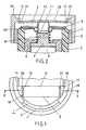
- the surge arrester shown in FIGS. 1 and 2 has a cylindrical housing 1 filled with an insulating agent, such as air, sulfur hexafluoride or insulating oil, and a pressure relief valve 2 which seals this housing from the outside in a gas-tight manner.
- the housing 1 can be made of metal, but can also - as shown - be formed from insulating material, such as porcelain or cast resin.
- the housing 1 is delimited on its end faces by two flanges of electrically conductive material fastened by means of a plastic compound 4 on the outside of the housing 1, of which the flange 3 shown in the figures has high voltage potential H.V. lies while the flange, not shown, is at ground potential or at a high voltage potential H.V. deviating potential.
- an active part 6 held by an insulating part 5 and consisting, for example, of a stack of non-linear metal oxide resistors.
- the active part 6 is electrically conductively connected to the pressure relief valve 2 via a contact element 7 and a flexible copper connection (not shown) and is located on the latter high end to high voltage HV Its lower (not shown) end is connected to earth or to a high voltage potential H.V. via a contact element (not shown) and the lower flange (not shown) of the housing 1. deviating potential.
- the individual resistors of the active part 6 contact each other with a force caused by a compression spring 8.
- the pressure relief valve 2 contains an annular cover 9 made of the lightest possible and electrically conductive material, such as aluminum, titanium or an alloy containing aluminum, titanium and / or vanadium.
- the edge of the cover 9 carries a sealing ring 10, which rests on the upper end face of the housing 1, which is designed as a sealing surface.
- the lid 9 also has an edge-stabilizing, in the interior of the housing 1 and eccentrically arranged embossment 11, in the outer cavity of which a sleeve 13 made of electrically conductive material, which is acted upon by a spiral spring 12 made of electrically conductive material, such as electrically conductive spring steel is stored.
- the compression spring 8 is supported with its upper end on the inward curvature formed by the impression 11. The lower end of the compression spring 8 is held by a projection of the contact element 7.
- the spiral spring 12 is designed as a bar and is supported with its two ends at two bearing points 14 and 15 attached to the flange 3. Between the two bearings 14 and 15, the spiral spring 12 has two material recesses, one of which is arranged in the region of the bearing 14 and the other in the region of the bearing 15. These material recesses can each be formed by a groove 16 or 17 which extends transversely to the longitudinal axis of the beam and transversely to the bending direction of the spiral spring 12 and which can be provided on the top and / or underside of the spiral spring 12. It is also conceivable that each material recess is formed in each case by two grooves which are respectively provided on the top and bottom of the spiral spring 12. As can be seen from the right-hand part of FIG.
- a groove 18 which is guided transversely to the longitudinal axis of the beam and which is essentially guided in the bending direction of the spiral spring 12, ie transversely to the groove 17.
- two alternatively on the front and back of the Bending spring 12 located and essentially in the bending direction of the bending spring 12 grooves 19, 20 may be provided.
- the material recesses are formed only by vertically guided grooves, such as the groove 18, 19 and / or 20.
- the grooves can only extend partially transversely to the spiral spring 12 without reaching the opposite sides thereof. It is also conceivable to design the material recesses as through bores or blind holes 21.
- the surge arrester shown above now acts as follows: In normal operating conditions, the end of the spiral spring 12 is supported on the bearing points 14 and 15 and exerts a force on the cover 9 via the sleeve 13 arranged in its center. A counterforce is exerted on the cover 9 by the compression spring 8 which is supported on the contact element 7 and acts on the resistances of the active part 6 with contact force, but which is considerably less than the force which can be generated with the spiral spring 12.
- the force of the spiral spring 12 is dimensioned such that the cover 9 closes the housing 1 filled with insulating material in a gas-tight manner.
- the spiral spring 12 may be subjected to the same high stress as a spiral spring without material recesses in the edge zone, since the smallest bending stress occurs in the edge zone and the greatest in the area of the acting force in the case of a flexible spring that is freely supported on both sides.
- the part of the active part 6 which is in contact with the contact element 7 is at high voltage potential via the contact element 7, the flexible copper connection (not shown), the cover 9, the sleeve 13, the spiral spring 12 and the bearing points 14 and 15 of the flange 3.
- a low operating current of at most a few mA (milliamperes) then flows through the arrester active part 6 to the flange of the housing 1, which is not shown, for example grounded, under normal operating conditions.
- an undesirable electric arc forms inside the housing 1, for example when unexpectedly high overvoltages occur or when one or more of the resistors of the active part is defective, this electric arc generates a pressure surge acting on the inner wall of the housing 1.
- the current feeding the arc is supplied to the arc by high voltage H.V. fed via the spiral spring 12.
- the parts of the spiral spring 12 which are located in the area of the bearing points 14 and 15 and have a small current-carrying cross section due to the grooves 16, 17, 18, 19 and / or 20 and the optionally provided bores or blind holes 21 (for example because of the skin effect ) considerably faster than the other parts of the spiral spring 12.
- the rigidity of the spiral spring 12 in the region of the material recesses is considerably reduced above a limit value of the current feeding the undesired arc. If a pressure surge caused by the arc is now formed in the housing, the pressure relief valve 2 reacts extremely quickly to this pressure surge and opens because of the comparatively low inertia of its cover 9 and because of the low rigidity of the spring at that time.
- the opening process is further accelerated in that the spiral spring 12 is arranged eccentrically with respect to the circular cover 9. Because of the eccentric arrangement, the spiral spring 12 is not only subjected to bending but also to torsion. Since, when the pressure surge occurs, the spring stiffness is significantly reduced with respect to both a bending and a torsional vibration, the cover 9 can therefore tilt very quickly and the interior of the housing 1 can be relieved of pressure in a predetermined desired direction.
Landscapes
- Engineering & Computer Science (AREA)
- Microelectronics & Electronic Packaging (AREA)
- Physics & Mathematics (AREA)
- Electromagnetism (AREA)
- Thermistors And Varistors (AREA)
- Gas-Insulated Switchgears (AREA)
Description
- Bei der Erfindung wird ausgegangen von einem Überspannungsableiter nach dem einleitenden Teil von Patentanspruch 1.
- Hierbei nimmt die Erfindung auf einen Stand der Technik von Hochspannungsapparaten Bezug, wie er etwa in der DE-A 3 032 852 beschrieben ist. Solche Überspannungsableiter weisen ein isoliergasgefülltes Gehäuse auf, in welchem ein an Hochspannung angeschlossener und aus einem Stapel von nichtlinearen Metalloxidwiderständen bestehender Aktivteil untergebracht ist. Das Gehäuse ist nach aussen durch Druckentlastungsventile abgeschlossen, welches oberhalb eines Grenzwertes des im Gehäuse befindlichen Isoliergases anspricht. Dieses Druckentlastungsventil weist einen kippbaren Deckel und eine auf diesem Deckel abgestützte Biegefeder auf und ist vergleichsweise träge.
- Aus FR-A 2 299 752 ist es bekannt, das Gehäuse eines Überspannungsableiters vor übermässiger Druckbelastung durch eine Druckbegrenzungsvorrichtung zu schützen. Diese Druckbegrenzungsvorrichtung weist eine das Gehäuse des Überspannungsabieiters nach aussen gasdicht abschliessende Membran sowie eine die Membran nach aussen abstützende und mit Sollbruchstellen versehene Halterung auf. Bei Auftreten eines unerwünscht hohen Überdruckes im Gehäuseinneren wird die Membran nach aussen bewegt und hierdurch die Halterung an den Sollbruchstellen zerstört. Die nunmehr ungestützte Membran reisst auf und entlastet hierbei das Gehäuse vom Überdruck.
- Die Erfindung, wie sie in dem unabhängigen Patenanspruch gekennzeichnet ist löst die Aufgabe, einen Hochspannungsapparat der eingangs genannten Art anzugeben, bei dem auch bei raschen Druckänderungen ine sichere Druckentlastung gewährleistet ist.
- Besondere Ausführungsarten der Erfindung sind in den abhängigen Patentansprüchen angegeben.
- Der Hochspannungsapparat nach der Erfindung zeichnet sich vor allem dadurch aus, dass unerwünschte Druckstösse abgebaut werden können, ohne dass das Gehäuse unzulässig belastet wird.
- Nachfolgend wird die Erfindung anhand der Zeichnung dargestellt. Hierbei zeigt:
- Fig. 1 eine Aufsicht auf eine als Ueberspannungsableiter ausgebildete Ausführungsform des Hochspannungsapparates nach der Erfindung, und
- Fig. 2 eine Aufsicht auf einen Schnitt längs 11-11 durch den Ueberspannungsableiter gemäss Fig. 1.
- Der in den Figuren 1 und 2 dargestellte Ueberspannungsableiter weist ein mit einem Isoliermittel, wie etwa Luft, Schwefelhexafluorid oder Isolieröl, gefülltes zylinderförmiges Gehäuse 1 sowie ein dieses Gehäuse nach aussen gasdicht abschliessendes Druckentlastungsventil 2 auf. Das Gehäuse 1 kann aus Metall bestehen, kann aber auch - wie dargestellt - aus Isoliermaterial, wie etwa Porzellan oder Giessharz gebildet sein. Das Gehäuse 1 wird an seinen Stirnseiten von zwei mittels einer Kunststoffmasse 4 auf der Aussenseite des Gehäuses 1 befestigten Flanschen aus elektrisch leitendem Material begrenzt, von denen der in den Figuren dargestellte Flansch 3 auf Hochspannungspotential H.V. liegt, während sich der nicht dargestellte Flansch auf Erdpotential befindet oder auf einem vom Hochspannungspotential H.V. abweichenden Potential. Im Inneren des Gehäuses 1 befindet sich ein von einem Isolierteil 5 gehaltenes und etwa aus einem Stapel nichtlinearer Metalloxidwiderstände bestehendes Aktivteil 6. Das Aktivteil 6 ist über ein Kontaktelement 7 und eine nicht dargestellte flexible Kupferverbindung mit dem Druckentlastungsventil 2 elektrisch leitend verbunden und befindet sich an seinem oberen Ende auf Hochspannung H.V. Sein unteres (nicht dargestelltes) Ende ist über ein (nicht dargestelltes) Kontaktelement und den (nicht dargestellten) unteren Flansch des Gehäuses 1 mit Erde oder mit einem vom Hochspannungspotential H.V. abweichenden Potential verbunden. Die einzelnen Widerstände des Aktivteils 6 kontaktieren einander mit einer durch eine Druckfeder 8 hervorgerufenen Kraft.
- Das Druckentlastungsventil 2 enthält einen kreisringförmigen Deckel 9 aus möglichst leichtem und elektrisch leitendem Material, wie etwa Aluminium, Titan oder einer Aluminium, Titan und/oder Vanadium enthaltenden Legierung. Der Rand des Deckels 9 trägt einen Dichtungsring 10, welcher auf der als Dichtungsfläche ausgebildeten oberen Stirnfläche des Gehäuses 1 aufliegt. Der Deckel 9 weist zudem eine seinen Rand stabilisierende, ins Innere des Gehäuses 1 gerichtete und exzentrisch angeordnete Einprägung 11 auf, in deren aussenliegendem Hohlraum eine von einer Biegefeder 12 aus elektrisch leitendem Material, wie etwa elektrisch leitendem Federstahl, beaufschlagte Hülse 13 aus elektrisch leitendem Material gelagert ist. Auf der von der Einprägung 11 gebildeten nach innen gerichteten Wölbung ist die Druckfeder 8 mit ihrem oberen Ende gelagert. Das untere Ende der Druckfeder 8 ist von einem Vorsprung des Kontaktelementes 7 gehalten.
- Die Biegefeder 12 ist als Balken ausgebildet und ist mit ihren beiden Enden an zwei am Flansch 3 angebrachten Lagerstellen 14 und 15 abgestützt. Zwischen beiden Lagerstellen 14 und 15 weist die Biegefeder 12 zwei Materialaus nehmungen auf, von denen die eine im Bereich der Lagerstelle 14 und die andere im Bereich der Lagerstelle 15 angeordnet ist. Diese Materialausnehmungen können jeweils von einer quer zur Balkenlängsachse und quer zur Biegerichtung der Biegefeder 12 erstreckten Nut 16 bzw. 17 gebildet sein, welche auf der Ober-und/oder Unterseite der Biegefeder 12 angebracht sein können. Es ist auch denkbar, dass jede Materialausnehmung jeweils von zwei jeweils auf der Ober-und Unterseite der Biegefeder 12 angebrachten Nuten gebildet ist. Wie aus dem rechten Teil der Fig. 1 ersichtlich ist, kann zusätzlich zur Nut 17 eine quer zur Balkenlängsachse geführte Nut 18 treten, welche im wesentlichen in Biegerichtung der Biegefeder 12, d.h. quer zur Nut 17 geführt ist. Wie in der linken Hälfte der Fig. 1 dargestellt ist, können alternativ auch zwei auf der Front- und Rückseite der Biegefeder 12 befindliche und im wesentlichen in Biegerichtung der Biegefeder 12 geführte Nuten 19, 20 vorgesehen sein. Es ist auch möglich, dass die Materialausnehmungen lediglich von vertikal geführten Nuten, wie etwa der Nut 18, 19 und/oder 20 gebildet sind. Ferner können sich die Nuten lediglich teilweise quer zur Biegefeder 12 erstrecken, ohne deren gegenüberliegenden Seiten zu erreichen. Auch ist es denkbar, die Materialausnehmungen als durchgehende Bohrungen oder Sacklöcher 21 auszubilden.
- Der vorstehend dargestellte Ueberspannungsableiter wirkt nun wie folgt: Bei normalen Betriebsbedingungen stützt sich die Biegefeder 12 mit ihren Enden auf den Lagerstellen 14 und 15 ab und übt über die in ihrer Mitte angeordnete Hülse 13 auf den Deckel 9 eine Kraft aus. Auf den Deckel 9 wird von der auf dem Kontaktelement 7 abgestützten und die Widerstände des Aktivteils 6 mit Kontaktkraft beaufschlagenden Druckfeder 8 eine Gegenkraft ausgeübt, welche jedoch wesentlich kleiner ist als die mit der Biegefeder 12 erzeugbare Kraft. Die Kraft der Biegefeder 12 ist so bemessen, dass der Deckel 9 das isoliermittelgefüllte Gehäuse 1 gasdicht abschliesst. Hierbei kann die Biegefeder 12 gegebenenfalls genauso hoch beansprucht werden wie eine Biegefeder ohne Materialausnehmungen in der Randzone, da bei einer beidseitig frei gelagerten Biegefeder die geringste Biegebeanspruchung in der Randzone und die grösste im Bereich der wirkenden Kraft auftritt. Zugleich befindet sich der am Kontaktelement 7 anliegende Teil des Aktivteils 6 über das Kontaktelement 7, die (nicht dargestellte) flexible Kupferverbindung, den Deckel 9, die Hülse 13, die Biegefeder 12 und die Lagerstellen 14 und 15 des Flansches 3 auf Hochspannungspotential. Durch das Ableiteraktivteil 6 fliesst dann bei normalen Betriebsbedingungen ein geringer Betriebsstrom von höchstens einigen mA (Milliampere) zum nicht dargestellten, beispielsweise geerdeten, Flansch des Gehäuses 1.
- Bildet sich unter bestimmten Voraussetzungen etwa beim Auftreten unerwartet hoher Ueberspannungen oder bei einem Defekt eines oder mehrerer der Widerstände des Aktivteils, ein unerwünschter Lichtbogen im Inneren des Gehäuses 1 aus, so erzeugt dieser Lichtbogen einen auf die Innenwand des Gehäuses 1 wirkenden Druckstoss. Der den Lichtbogen speisende Strom wird dem Lichtbogen von Hochspannung H.V. über die Biegefeder 12 zugeführt. Hierbei erwärmen sich die im Bereich der Lagerstellen 14 und 15 befindlichen und wegen der Nuten 16, 17, 18, 19 und/oder 20 sowie der gegebenenfalls vorgesehenen Bohrungen bzw. Sacklöcher 21 einen geringen stromdurchflossenen Querschnitt aufweisenden Teile der Biegefeder 12 (etwa wegen des Skineffektes) erheblich rascher als die übrigen Teile der Biegefeder 12. Hierdurch wird die Steifigkeit der Biegefeder 12 im Bereich der Materialausnehmungen oberhalb eines Grenzwertes des den unerwünschten Lichtbogen speisenden Stroms erheblich herabge setzt. Bildet sich nun ein durch den Lichtbogen hervorgerufener Druckstoss im Gehäuse aus, so reagiert das Druckentlastungsventil 2 wegen der vergleichsweise geringen Trägheit seines Deckels 9 und wegen der zu diesem Zeitpunkt geringen Steifigkeit der Feder äusserst rasch auf diesem Druckstoss und öffnet.
- Der Oeffnungsvorgang wird noch dadurch beschleunigt, dass die Biegefeder 12 exzentrisch hinsichtlich des kreisrunden Deckels 9 angeordnet ist. Durch die exzentrische Anordnung wird nämlich die Biegefeder 12 nicht nur auf Biegung sondern zusätzlich auch auf Torsion beansprucht. Da bei Auftreten des Druckstosses die Federsteifigkeit sowohl hinsichtlich einer Biegungs- als auch einer Torsionsschwingung wesentlich herabgesetzt ist, kann daher der Deckel 9 zugleich sehr rasch kippen und das Innere des Gehäuses 1 in einer vorgegebenen erwünschten Richtung von Druck entlastet werden.
Claims (7)
Applications Claiming Priority (2)
| Application Number | Priority Date | Filing Date | Title |
|---|---|---|---|
| CH1627/86 | 1986-04-22 | ||
| CH162786 | 1986-04-22 |
Publications (2)
| Publication Number | Publication Date |
|---|---|
| EP0243813A1 EP0243813A1 (de) | 1987-11-04 |
| EP0243813B1 true EP0243813B1 (de) | 1990-07-04 |
Family
ID=4214864
Family Applications (1)
| Application Number | Title | Priority Date | Filing Date |
|---|---|---|---|
| EP87105651A Expired - Lifetime EP0243813B1 (de) | 1986-04-22 | 1987-04-16 | Überspannungsableiter |
Country Status (5)
| Country | Link |
|---|---|
| US (1) | US4766513A (de) |
| EP (1) | EP0243813B1 (de) |
| JP (1) | JPH0828924B2 (de) |
| CA (1) | CA1298869C (de) |
| DE (1) | DE3763526D1 (de) |
Families Citing this family (1)
| Publication number | Priority date | Publication date | Assignee | Title |
|---|---|---|---|---|
| DE102011007677A1 (de) * | 2011-04-19 | 2012-10-25 | Siemens Aktiengesellschaft | Ausblasschute und Überspannungsableiter |
Family Cites Families (4)
| Publication number | Priority date | Publication date | Assignee | Title |
|---|---|---|---|---|
| FR1083228A (fr) * | 1952-09-10 | 1955-01-06 | Oerlikon Maschf | Parafoudre |
| DE2247997C3 (de) * | 1972-09-27 | 1978-05-11 | Siemens Ag, 1000 Berlin Und 8000 Muenchen | Überspannungsableiter mit isolierendem Gehäuse |
| FR2299752A1 (fr) * | 1974-06-19 | 1976-08-27 | Alsthom Cgee | Parafoudre |
| DE3032852A1 (de) * | 1980-04-29 | 1981-11-05 | BBC AG Brown, Boveri & Cie., 5401 Baden, Aargau | Ueberspannungsableiter |
-
1987
- 1987-04-13 CA CA000534565A patent/CA1298869C/en not_active Expired - Lifetime
- 1987-04-15 US US07/038,617 patent/US4766513A/en not_active Expired - Lifetime
- 1987-04-16 DE DE8787105651T patent/DE3763526D1/de not_active Expired - Lifetime
- 1987-04-16 EP EP87105651A patent/EP0243813B1/de not_active Expired - Lifetime
- 1987-04-22 JP JP62097658A patent/JPH0828924B2/ja not_active Expired - Lifetime
Also Published As
| Publication number | Publication date |
|---|---|
| DE3763526D1 (de) | 1990-08-09 |
| EP0243813A1 (de) | 1987-11-04 |
| CA1298869C (en) | 1992-04-14 |
| US4766513A (en) | 1988-08-23 |
| JPS62254609A (ja) | 1987-11-06 |
| JPH0828924B2 (ja) | 1996-03-21 |
Similar Documents
| Publication | Publication Date | Title |
|---|---|---|
| DE19739375B4 (de) | Öffnungsvorrichtung für einen Gasdruckbehälter eines Airbags | |
| EP0484703A2 (de) | Elektrische Sicherung | |
| EP0132634B1 (de) | Elektrischer Kondensator mit Überdruckabreisssicherung | |
| DE1295071B (de) | Sicherung fuer elektrische Kondensatoren | |
| DE102017207629B4 (de) | Anordnung mit einer Gasdruckfeder für eine Seil-Rotationspendel-Kinematik und Verwendung der Anordnung zum Schalten | |
| EP0789434A1 (de) | Verfahren zur Beeinflussung des Folgestromlöschvermögens von Funkenstreckenanordnungen und Funkenstreckenanordnungen hierfür | |
| DE102018100076B3 (de) | Kurzschließeinrichtung für den Einsatz in Nieder- und Mittelspannungsanlagen zum Sach- und Personenschutz | |
| EP1604138A1 (de) | Druckentlastungsventil | |
| EP0243813B1 (de) | Überspannungsableiter | |
| DE2741022C2 (de) | Elektrischer Druckgasschalter | |
| DE3227339C2 (de) | Schnellantriebsvorrichtung für einen Schnellerder | |
| DE2247997C3 (de) | Überspannungsableiter mit isolierendem Gehäuse | |
| DE969871C (de) | Leistungsschalter mit zentripetaler Beblasung des Lichtbogens und zylindrische Form aufweisenden Kontakten | |
| DE1058601B (de) | Elektrischer Schalter | |
| EP2156444A1 (de) | Überspannungsableiteranordnung | |
| DE1290241B (de) | UEberspannungsableiter | |
| DE4041979C2 (de) | ||
| DE2619317A1 (de) | Blitzschutzvorrichtung | |
| DE824228C (de) | UEberspannungsschutzsicherung | |
| DE102006048977B4 (de) | Gekapselte, druckfest ausgeführte, nicht hermetisch dichte, rotationssymmetrische Hochleistungsfunkenstrecke | |
| DE941505C (de) | Fluessigkeitsschalter | |
| DE2928965A1 (de) | Elektrischer kondensator | |
| DE1935190C (de) | Funkenstreckenanordnung für Überspannungsableiter, insbesondere für Gleichstrom-Überspannungsableiter | |
| DE2304338A1 (de) | Ausdehnungskoerper fuer hochspannungsgeraete | |
| DE1515595C3 (de) | Elektrischer Sprungschalter |
Legal Events
| Date | Code | Title | Description |
|---|---|---|---|
| PUAI | Public reference made under article 153(3) epc to a published international application that has entered the european phase |
Free format text: ORIGINAL CODE: 0009012 |
|
| AK | Designated contracting states |
Kind code of ref document: A1 Designated state(s): CH DE FR GB LI SE |
|
| 17P | Request for examination filed |
Effective date: 19880422 |
|
| 17Q | First examination report despatched |
Effective date: 19890322 |
|
| GRAA | (expected) grant |
Free format text: ORIGINAL CODE: 0009210 |
|
| AK | Designated contracting states |
Kind code of ref document: B1 Designated state(s): CH DE FR GB LI SE |
|
| REF | Corresponds to: |
Ref document number: 3763526 Country of ref document: DE Date of ref document: 19900809 |
|
| ET | Fr: translation filed | ||
| GBT | Gb: translation of ep patent filed (gb section 77(6)(a)/1977) | ||
| PLBE | No opposition filed within time limit |
Free format text: ORIGINAL CODE: 0009261 |
|
| STAA | Information on the status of an ep patent application or granted ep patent |
Free format text: STATUS: NO OPPOSITION FILED WITHIN TIME LIMIT |
|
| 26N | No opposition filed | ||
| PGFP | Annual fee paid to national office [announced via postgrant information from national office to epo] |
Ref country code: SE Payment date: 19930322 Year of fee payment: 7 |
|
| PG25 | Lapsed in a contracting state [announced via postgrant information from national office to epo] |
Ref country code: SE Effective date: 19940417 |
|
| EUG | Se: european patent has lapsed |
Ref document number: 87105651.1 Effective date: 19941110 |
|
| PGFP | Annual fee paid to national office [announced via postgrant information from national office to epo] |
Ref country code: GB Payment date: 20000313 Year of fee payment: 14 |
|
| PGFP | Annual fee paid to national office [announced via postgrant information from national office to epo] |
Ref country code: DE Payment date: 20000320 Year of fee payment: 14 |
|
| PGFP | Annual fee paid to national office [announced via postgrant information from national office to epo] |
Ref country code: CH Payment date: 20000323 Year of fee payment: 14 |
|
| PGFP | Annual fee paid to national office [announced via postgrant information from national office to epo] |
Ref country code: FR Payment date: 20000327 Year of fee payment: 14 |
|
| PG25 | Lapsed in a contracting state [announced via postgrant information from national office to epo] |
Ref country code: GB Free format text: LAPSE BECAUSE OF NON-PAYMENT OF DUE FEES Effective date: 20010416 |
|
| PG25 | Lapsed in a contracting state [announced via postgrant information from national office to epo] |
Ref country code: FR Free format text: THE PATENT HAS BEEN ANNULLED BY A DECISION OF A NATIONAL AUTHORITY Effective date: 20010430 |
|
| PG25 | Lapsed in a contracting state [announced via postgrant information from national office to epo] |
Ref country code: LI Free format text: LAPSE BECAUSE OF NON-PAYMENT OF DUE FEES Effective date: 20010515 Ref country code: CH Free format text: LAPSE BECAUSE OF NON-PAYMENT OF DUE FEES Effective date: 20010515 |
|
| GBPC | Gb: european patent ceased through non-payment of renewal fee |
Effective date: 20010416 |
|
| REG | Reference to a national code |
Ref country code: CH Ref legal event code: PL |
|
| PG25 | Lapsed in a contracting state [announced via postgrant information from national office to epo] |
Ref country code: DE Free format text: LAPSE BECAUSE OF NON-PAYMENT OF DUE FEES Effective date: 20020201 |
|
| REG | Reference to a national code |
Ref country code: FR Ref legal event code: ST |
|
| REG | Reference to a national code |
Ref country code: CH Ref legal event code: AUV Free format text: DAS OBENGEANNNTE PATENTGESUCH IST, MANGELS BEZAHLUNG DER 15. JAHRESGEBUEHR ZURUECKGEWIESEN WORDEN. |