EP0243639A2 - System zur automatischen Inspektion periodischer Muster - Google Patents
System zur automatischen Inspektion periodischer Muster Download PDFInfo
- Publication number
- EP0243639A2 EP0243639A2 EP87103634A EP87103634A EP0243639A2 EP 0243639 A2 EP0243639 A2 EP 0243639A2 EP 87103634 A EP87103634 A EP 87103634A EP 87103634 A EP87103634 A EP 87103634A EP 0243639 A2 EP0243639 A2 EP 0243639A2
- Authority
- EP
- European Patent Office
- Prior art keywords
- pixel
- pixels
- test
- values
- image
- Prior art date
- Legal status (The legal status is an assumption and is not a legal conclusion. Google has not performed a legal analysis and makes no representation as to the accuracy of the status listed.)
- Granted
Links
Images


Classifications
-
- G—PHYSICS
- G06—COMPUTING OR CALCULATING; COUNTING
- G06T—IMAGE DATA PROCESSING OR GENERATION, IN GENERAL
- G06T7/00—Image analysis
- G06T7/0002—Inspection of images, e.g. flaw detection
- G06T7/0004—Industrial image inspection
- G06T7/001—Industrial image inspection using an image reference approach
-
- G—PHYSICS
- G03—PHOTOGRAPHY; CINEMATOGRAPHY; ANALOGOUS TECHNIQUES USING WAVES OTHER THAN OPTICAL WAVES; ELECTROGRAPHY; HOLOGRAPHY
- G03F—PHOTOMECHANICAL PRODUCTION OF TEXTURED OR PATTERNED SURFACES, e.g. FOR PRINTING, FOR PROCESSING OF SEMICONDUCTOR DEVICES; MATERIALS THEREFOR; ORIGINALS THEREFOR; APPARATUS SPECIALLY ADAPTED THEREFOR
- G03F7/00—Photomechanical, e.g. photolithographic, production of textured or patterned surfaces, e.g. printing surfaces; Materials therefor, e.g. comprising photoresists; Apparatus specially adapted therefor
- G03F7/70—Microphotolithographic exposure; Apparatus therefor
- G03F7/70483—Information management; Active and passive control; Testing; Wafer monitoring, e.g. pattern monitoring
- G03F7/70605—Workpiece metrology
- G03F7/70616—Monitoring the printed patterns
- G03F7/7065—Defects, e.g. optical inspection of patterned layer for defects
-
- G—PHYSICS
- G06—COMPUTING OR CALCULATING; COUNTING
- G06T—IMAGE DATA PROCESSING OR GENERATION, IN GENERAL
- G06T2207/00—Indexing scheme for image analysis or image enhancement
- G06T2207/30—Subject of image; Context of image processing
- G06T2207/30108—Industrial image inspection
- G06T2207/30141—Printed circuit board [PCB]
-
- G—PHYSICS
- G06—COMPUTING OR CALCULATING; COUNTING
- G06T—IMAGE DATA PROCESSING OR GENERATION, IN GENERAL
- G06T2207/00—Indexing scheme for image analysis or image enhancement
- G06T2207/30—Subject of image; Context of image processing
- G06T2207/30108—Industrial image inspection
- G06T2207/30148—Semiconductor; IC; Wafer
Definitions
- This invention relates to a method and apparatus for the automatic inspection of periodic patterns such as memory arrays and programmable logic arrays in integrated circuit chips and the like. More particularly, this invention relates to a method and apparatus for the automatic inspection of periodic patterns in the above devices wherein the known periodicity of the pattern is used to identify defects by comparing repetitive cells in the periodic array.
- Koniski et al technique consists of applying an edge detector to a greyscale image and then detecting defects by comparing edge points with their periodic counterparts one repetition period away. The lack of a match indicates the presence of a defect.
- the technique is quite noise sensitive and many of the details of implementation address the problem of suppressing false defect calls due to noise.
- the result is a technique that, is only capable of detecting defects much larger than the pixel size. Suspected defects points are found by a comparison between edge points and their counterparts one repetition period away. A suspected defect would be indicated, in this case, by a "1-10" comparison result. Using this suspected defect procedure to make the final defect determination would, however, produce unacceptable high false call rates due to noise effects, which are still present at this point in spite of the large gradient operator used.
- a method and apparatus for automatic inspection of periodic patterns typically found on patterned silicon wafers, printed circuit board, and/or mask for photolithography is disclosed.
- the method comprises an inspection algorithm of two parts: a low-level algorithm and a higher level algorithm which includes, therein the operation of the low-level algorithm.
- the low-level algorithm utilizes the known periodicity of the pattern to find defects by comparing supposedly identical cells in the periodic array.
- the low-level algorithm assumes horizontal (in the image) periodicity only and analyzes the greyscale identity for each pixel in the image (except those in a dead zone along the borders) by comparing it with the greyscale identity for the two pixel neighborhood, which are a pattern repetition period, R, away in either direction.
- the low-level algorithm includes an edge detector applied in the neighborhoods of the compared pixels and a missing pattern test for identifying vacant patterns in the array.
- the high-level algorithm comprises applying the low-level algorithm, some number of times (N) in succession on the image.
- An accumulator image is formed by adding the results of the low-level algorithm to create a separate image array where the pixels relate to the number of times that the pixel in the original image was detected as defective by the low-level algorithm.
- the apparatus for implementing the above method first comprises a means for digitizing a video signal of the periodic array such that the output of said means is a digital greyscale image, read out in raster scan fashion. The image then goes into a dual ported high speed memory means where the previously stored image is being read out and passed to a means for performing the method of the low-level algorithm.
- This low-level algorithm means takes the greyscale image as input and produces a corresponding binary image where the ones represent suspected defect pixels and the zeros do not. This image then passes to a means that converts the binary image into a list of the image coordinates of the ones. This constitutes a valuable form of data compression since the binary image will normally be sparse. In fact, the majority of the time it will be all zeros. These coordinates are then read over the computer bus by the micro-computer, which uses them to update the accumulator array. Once the N iterations of the low-level algorithm have been executed using this pipeline, the micro-computer determines where the defective pixels (if any) are located using the high-level algorithm. The results can then be displayed to the operator by modifying those pixels in the image stored in the frame buffer, and then displaying that image on a video monitor via a D/A converter (shown as part of the frame grabber).
- digital greyscale data enters into a delay line, which provides the fifteen pixels in parallel to a network that routes the values to the appropriate inputs of the various subtract-and-compare units (SACS).
- SACS subtract-and-compare units
- Each of the SACs produces a boolean result and are implemented by look-up table RAMs.
- the results are combined by a logic network that also includes two missing pattern tests.
- the final result of the boolean combinations is a single boolean value, which constitutes one pixel in a binary image in this case.
- FIG. 1 A block diagram of the inspection system is shown in FIG. 1.
- an automated inspection station providing microscope optics and computer controlled wafer handling means as well as microscope function control for things like light intensity and autofocus offset.
- Low numerical aperture illumination is used to maximize contrast and a solid state video camera (for low geometric distortion) is mounted on the trinocular microscope head.
- the camera is used by the image analysis hardware and software for performing the actual inspection operation.
- the camera's video signal is split, one part going to special image analysis electronics as part of the image computer where the signal is digitized and analyzed as will be described below.
- the entire system is controlled by the micro-computer (shown in FIG. 8) which also performs the inspection algorithms.
- the image analysis part of the system uses a high speed video pipeline to do the processing.
- the analog signal coming from the video camera is digitized in one frame time (for RS 170 this is 0.033 sec) and fed to the rest of the pipeline at a rate of 10 megapixels per second. This produces a 512 ⁇ 512 pixel digital image. In all discussions that follow this particular image form will be assumed.
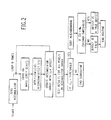
- FIG. 2 there is shown a flow chart for the high-level algorithm of the inspection system.
- digital images of the same optical image are acquired some number of times N.
- a low-level defect test (to be described below) is applied to each of these images. This test produces a binary image where ones correspond to suspected defect pixels and all other pixels are set to zero.
- the results of the low-level tests are added to an accumulator image (array) corresponding pixel-wise to the digital images.
- the pixels in the accumulator image will contain values ranging from 0 to N.
- each box represents a matrix of 3 ⁇ 3 pixels or nine pixel group.
- Each number N in the matrix corresponding to the number of times a certain pixel was indicated as a suspected defect.
- the high-level algorithm applies a statistical test to the pixels of the accumulator image containing sums of low-level test results for N iterations.
- this test is simply an identity operation on the low-level test result.
- the false detection rate can be significantly reduced (with little effect on the defect escape rate) by applying the low-level test several times in succession.
- the simplest form of the high-level algorithm for multiple digitizations is to apply a threshold to the accumulator image, causing those pixels that had "true" test results at least N H (count threshold for the high level test) times to be called defective.
- a general form of the high-level algorithm involves not only the pixel under test but its eight nearest neighbors as well.
- the primary purpose of this test is to handle another type of false defect which is due to real but acceptable differences in the pattern being inspected.
- An example of this might be something like a texture (mottled) background which is often referred to using names like "orange peel".
- the following parameters applied by the low-level algorithm allows the trade-off between the smallest detectable defect size and false detection rates in such cases.
- the pixels of the neighborhood comprising the pixel under test and its eight nearest neighbors can be ranked and the sum, S, of the largest number of pixels considered in the high-level algorithm is compared with the threshold N H . If S is greater than or equal to N H then the central pixel is called a defect.
- the following is a list of the parameters of the low-level algorithm for controlling the identification of defects by the high-level algorithm.
- the low-level algorithm utilizes the known periodicity of the pattern to find defects by comparing supposedly identical cells in the periodic array.
- the low-level algorithm assumes horizontal (in the image) periodicity only and analyzes each pixel in the image (except those in a dead zone along the borders) by comparing it with the two pixels one pattern repetition period, R, away in either direction.
- the pixel under test is compared with periodic neighbors on either side in order to determine which pixel is defective when an error is detected. This also produces the benefit of eliminating false defect detection due to slowly varying illumination (shading). If the array being inspected and the images of its being analyzed could be assumed perfectly periodic except for defects, then the inpsection algorithm could consist of simply comparing the pixel under test with these two pixels and flagging detected differences as defects.
- the realities of acceptable pattern differences and image acquisition szstem noise and distortion require a considerably more complicated algorithm, however.
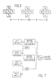
- FIG. 4 a supplied flow for the low-level algorithm is shown. From the FIG. 4, it can be seen that if a pixel is blacker than both its left and right neighbors R pixels away or if it is whiter than both of those neighbors, then its called a suspected defect and assigned a "1" in the binary image.
- the terms "blacker than” and “whiter than” will be defined more precisely as this description progresses.
- Fig. 5 is a graphic depiction of fifteen pixels used in one embodiment of an inspection scheme for the low-level algorithm.
- FIG. 5 The notation used in FIG. 5 will be used throughout this discussion.
- the pixel under test is the one labeled c0 while its left and right periodic neighbors are labeled 10 and r0 respectively.
- the three five connected pixel groups in FIG. 5 will be referred to as the left hand, central and right hand crosses.
- Each of the four tests shown in FIG. 4 is composed of a boolean combination of the results of 18 subtract-and-compare operations as depicted in FIG. 6, which is one of these combinations (left/black) expanded.
- Each subtract-and-compare operation consists of taking the difference between two pixel grey levels and comparing it or its absolute value with a threshold, thus producing a boolean result.
- the result of each of the four tests is obtained by ORing the results of three sub-tests, each of which may be further decomposed into two tests. From top to bottom in the FIGURE, the three tests are: high sensitivity comparison test, horizontal row test and vertical row test. As the name implies the high sensitivity test is the most sensitive, having the smallest grey-level comparison threshold, but it gives false indications in regions of high gradient (i.e. on edges). The solution to this is to "turn off" the test in regions of high gradient.
- the two tests making up the high sensitivity test are:
- the horizontal row test is somewhat lower sensitivity, but is capable of detecting defects on horizontally oriented edges. This test result is formed by ANDing the results of the following two tests:
- the vertical row test is identical in structure to the horizontal row test, except that it considers north-south pixels.
- the central pixel is compared with several pixels (either 5 or 3) in one of the side crosses to ensure that random variations do not cause a false detection. In both these cases it is assumed that there is little variation within the pixels being compared with the central pixel. In the difference test a uniform area is assumed while in the side row test the pixels are assumed to lie along a greyscale contour line parallel to an edge.
- the missing pattern test is performed by tracking the results of the left/black and right/black tests and flagging a suspected defect if either test result is true for some number, N M , of horizontally consecutive pixels. More precisely, a counter is maintained for each of the two black tests. Each time the test result is true, the counter is incremented and every time the result is false the counter is cleared (set to zero). The counters are examined after each iteration and the current pixel under test, c0, is flagged (set to one) if the counter value is greater than or equal to N M .
- FIG. 8 there is a block diagram of the image analysis electronics of this invention.
- a high speed video pipeline is shown where data flows from left to right to the FIGURE.
- this pipeline will be referred to as the image computer.
- the modules are linked by high speed 8 bit wide data paths and they are also all attached to a computer bus along with a micro-computer that controls the modules via the bus as well as performing the high-level algorithm and controlling the rest of the system.
- the modules all operate in parallel in typical pipeline fashion.
- the video signal is first digitized by a high speed analog-to-digital converter frame grabber, whose output is a digital greyscale image, read out in raster scan fashion. This image then goes into a dual ported high speed memory frame buffer, while the previous image is being read out and passed to a module that performs the low-level algorithm as described above.
- the frame buffer is not required for the automatic inspection process, but it is needed for the review phase where the system uses the buffer to display the inspection results.
- the low level algorithm therefore, takes the greyscale image as input and produces a corresponding binary image where the ones represent suspected defect pixels and the zeros do not. This image then passes to a module that converts the binary image into a list of the image coordinates of the ones. This constitutes a valuable form of data compression since the binary image will normally be sparse. In fact the majority of the time it will be all zeros. These coordinates are then read over the computer bus by the micro-computer, which uses them to update the accumulator array. Once the N iterations of the low-level algorithm have been executed using this pipeline the micro-computer determines where the defective pixels (if any) are located using the high-level algorithm. The results can then be displayed to the operator by modifying those pixels in the image stored in the frame buffer, and then displaying that image on a video monitor via a D/A converter (shown as part of the frame grabber).
- the image computer is programmed by the micro-computer as follows. First, when a new product/level is to be inspected, the low-level algorithm module is programmed with the pattern repetition period and the various thresholds. Then, once the microscope stage has been stepped so that a new image may be acquired and analyzed, all the boards are put in "continuous" mode which means that images are continuously acquired and passed through the pipeline at video rate (30 frames/sec). This must be done in a way that causes N images to be processed and the system to then stop. Once the last image of a given set has been acquired, the system control program may then step the stage to the next field to be processed. While the stage is moving the last image is processed by the image computer and the micro-computer performs the high-level algorithm test. There must also be some synchronization between the feature extractor processing and the micro-computer, so that the micro-computer can retrieve the detected pixel locations before the next frame has been processed.
- FIG. 8 While the overall structure described in FIG. 8 is unique for this system, versions of all but one of the individual modules shown may be obtained commercially. This unique module is the low-level algorithm module. The operational structure of that module is essentially given by FIG. 4. Each of the four boxes in this FIGURE and the missing pattern test will be expanded and described in detail below.
- FIG. 10 One scheme for partitioning the low-level algorithm module is shown in FIG. 10.
- This FIGURE shows digital greyscale data entering a delay line, which provides the fifteen pixels in parallel to a network that routes the values to the appropriate inputs of the various subtract-and-compare units (SACs).
- SACs subtract-and-compare units
- Each of the SACs produces a boolean result.
- An analysis of the algorithm shows that there is a total of 56 unique results of this type, which are combined by a logic network that also includes the two missing pattern tests.
- the final result of the boolean combinations is a single boolean value, which constitutes one pixel in a binary image in this case.
- the fifteen pixels shown in FIG. 5 must all be available simultaneously. In the invention, this will be achieved using a delay line with fifteen taps. For a given pattern repetition period the delay line must be 2M+2R long, where M is the number of pixels per scan (512 in this case). For flexible use the tap locations must be programmable and the delay line must be 2M+2R max long. Such a delay might be implemented by stringing together programmable first-in-first-out memories (FIFOs) or by using programmable counters to address a RAM buffer, for example.
- FIFOs programmable first-in-first-out memories
- a LUT may be used to implementing any boolean function of two greyscale variables, by applying the two n-bit greyscale values to the address lines of a 2 2n ⁇ 1 bit RAM while asserting the "read" line, thus producing the boolean result (which had been previously stored in the RAM) on the "data" line.
- the advantages of this implementation are the reduced chip count (1 for LUT vs. at least 3 for subtracters, comparators, etc.) and increased flexibility (any boolean function of two greyscale variables may be programmed).
- the primary disadvantage is that programming a detection threshold requires programming an entire RAM. A scheme for doing this programming in a minimal amount of time will be described below. The LUT scheme will be embodied herein.
- the missing pattern test fits in with the rest of the low-level algorithm as shown in FIG. 7. As described in relation thereto, its function is to count positive results from either of the black tests, producing a positive output whenever it has encountered N M consecutive positive inputs. A possible implementation of this is shown in FIG. 11.
- a preset value is loaded into a self-presetting counter.
- true inputs enable the counter, allowing it to count clock pulses.
- the logic shown causes the D flip-flop's Q output to be asserted indicated a true result for the missing pattern test. As long as the circuit's input remains true, Q will remain true. As soon as the input goes false, however, the counter will be cleared/preset and Q will become false and stay false until the counter overflows again.
- the low-level algorithm module must be programmed by the micro-computer with the pattern repetition period, R, the three comparison threshold T D , T G and T R , and the count threshold for the mission pattern test, N M .
- the repetition period and the missing pattern test count threshold will be programmable by loading a presettable counter or some equally simple operation. If subtracters and comparators are used to implement the SACs, then programming the comparison thresholds is also a simple matter, consisting of simply loading a set of registers from the micro-computer bus.
- the comparison threshold will not be as simple to program, however, when using the LUT implementation, because of the need to program an entire RAM look-up table. The following is a description of a circuit and associated scheme for programming these LUTs in an efficient manner.
- the only access provided to the RAM address lines is through the delay line taps, which provide the pixel greyscale values during run mode.
- the only way for the micro-computer can place values there is by loading them into the frame buffer via the computer bus and then clocking them into the low-level algorithm module delay line over the high speed video bus. While the LUTs could be programmed this way, in principle, it would be a very complicated and time consuming process.
- This multiplexing scheme may be greatly simplified for all but the gradient test LUTs by multiplexing the delay line taps in the routing network rather than multiplexing the RAM address lines directly.
- FIG. 12 shows one LUT from the left-black test (l E -c0I>T D ) and its associated delay line taps and multiplexors (MUXs). This works because these LUTs involve a difference between c0 and some other pixel.
- the multiplexing scheme can multiplex the c0 tap with another set of lines (greyscale value) coming from the computer bus and all other taps can be multiplexed with another single value (call it "ee" for "everything else”).
- the various signal lines shown in the FIGURE and their function during the run and program modes may be described as follows:
Landscapes
- Engineering & Computer Science (AREA)
- Physics & Mathematics (AREA)
- General Physics & Mathematics (AREA)
- Quality & Reliability (AREA)
- Computer Vision & Pattern Recognition (AREA)
- Theoretical Computer Science (AREA)
- Investigating Materials By The Use Of Optical Means Adapted For Particular Applications (AREA)
- Testing Or Measuring Of Semiconductors Or The Like (AREA)
- Image Processing (AREA)
- Image Analysis (AREA)
- Length Measuring Devices By Optical Means (AREA)
Applications Claiming Priority (2)
| Application Number | Priority Date | Filing Date | Title |
|---|---|---|---|
| US853100 | 1986-04-17 | ||
| US06/853,100 US4771468A (en) | 1986-04-17 | 1986-04-17 | System for automatic inspection of periodic patterns |
Publications (3)
| Publication Number | Publication Date |
|---|---|
| EP0243639A2 true EP0243639A2 (de) | 1987-11-04 |
| EP0243639A3 EP0243639A3 (de) | 1991-01-02 |
| EP0243639B1 EP0243639B1 (de) | 1994-07-13 |
Family
ID=25315048
Family Applications (1)
| Application Number | Title | Priority Date | Filing Date |
|---|---|---|---|
| EP87103634A Expired - Lifetime EP0243639B1 (de) | 1986-04-17 | 1987-03-13 | System zur automatischen Inspektion periodischer Muster |
Country Status (4)
| Country | Link |
|---|---|
| US (1) | US4771468A (de) |
| EP (1) | EP0243639B1 (de) |
| JP (1) | JPH0799547B2 (de) |
| DE (1) | DE3750189T2 (de) |
Cited By (3)
| Publication number | Priority date | Publication date | Assignee | Title |
|---|---|---|---|---|
| GB2253697A (en) * | 1991-03-13 | 1992-09-16 | Secr Defence | Image anomaly detector |
| FR2701766A1 (fr) * | 1993-02-17 | 1994-08-26 | Inst Textile De France | Procédé d'acquisition et de traitement de l'image d'un article plan, du type étoffe de tissu, en vue de la détection de défauts de fabrication. |
| WO2006012914A1 (en) * | 2004-08-05 | 2006-02-09 | Icos Vision System N.V. | Method for inspecting surfaces |
Families Citing this family (22)
| Publication number | Priority date | Publication date | Assignee | Title |
|---|---|---|---|---|
| JPH01224881A (ja) * | 1988-03-04 | 1989-09-07 | Toshiba Mach Co Ltd | パターン検査装置 |
| US5091963A (en) * | 1988-05-02 | 1992-02-25 | The Standard Oil Company | Method and apparatus for inspecting surfaces for contrast variations |
| US5040056A (en) * | 1990-01-29 | 1991-08-13 | Technistar Corporation | Automated system for locating and transferring objects on a conveyor belt |
| US5041907A (en) * | 1990-01-29 | 1991-08-20 | Technistar Corporation | Automated assembly and packaging system |
| US5062714A (en) * | 1990-02-12 | 1991-11-05 | X-Rite, Incorporated | Apparatus and method for pattern recognition |
| US5193690A (en) * | 1991-06-06 | 1993-03-16 | Western Litho Plate & Supply Co. | Method of and apparatus for automatically inspecting an exposed and bent lithographic plate |
| US5352189A (en) * | 1992-02-19 | 1994-10-04 | Tecnol Medical Products, Inc. | Ankle brace walker |
| US5513275A (en) * | 1993-01-12 | 1996-04-30 | Board Of Trustees Of The Leland Stanford Junior University | Automated direct patterned wafer inspection |
| JP3246704B2 (ja) * | 1995-02-27 | 2002-01-15 | シャープ株式会社 | 配線基板の検査装置 |
| US5917935A (en) * | 1995-06-13 | 1999-06-29 | Photon Dynamics, Inc. | Mura detection apparatus and method |
| JP3566470B2 (ja) * | 1996-09-17 | 2004-09-15 | 株式会社日立製作所 | パターン検査方法及びその装置 |
| US6023680A (en) * | 1997-05-15 | 2000-02-08 | Panasonic Technologies, Inc. | Methods, apparatus and computer program products for automated visual inspection |
| US6674888B1 (en) * | 1998-02-27 | 2004-01-06 | Applied Materials, Inc. | Tuning method for a processing machine |
| JP3152203B2 (ja) * | 1998-05-27 | 2001-04-03 | 株式会社東京精密 | 外観検査装置 |
| US6324298B1 (en) | 1998-07-15 | 2001-11-27 | August Technology Corp. | Automated wafer defect inspection system and a process of performing such inspection |
| US6459448B1 (en) | 2000-04-19 | 2002-10-01 | K-G Devices Corporation | System and method for automatically inspecting arrays of geometric targets |
| KR100515491B1 (ko) * | 2001-12-07 | 2005-09-16 | 다이닛뽕스크린 세이조오 가부시키가이샤 | 반도체 기판 상의 패턴을 검사하는 장치와 방법 및 컴퓨터판독 가능한 기록매체 |
| JP2004333386A (ja) * | 2003-05-09 | 2004-11-25 | Nec Corp | レチクル検査装置及びレチクル検査方法 |
| EP1697729B1 (de) * | 2003-09-04 | 2010-11-10 | KLA-Tencor Corporation | Verfahren zur inspektion einer probe unter verwendung unterschiedlicher inspektionsparameter |
| JP5566265B2 (ja) * | 2010-11-09 | 2014-08-06 | 東京エレクトロン株式会社 | 基板処理装置、プログラム、コンピュータ記憶媒体及び基板の搬送方法 |
| US9494856B1 (en) * | 2011-06-07 | 2016-11-15 | Hermes Microvision, Inc. | Method and system for fast inspecting defects |
| US10043259B2 (en) | 2016-07-25 | 2018-08-07 | PT Papertech Inc. | Facilitating anomaly detection for a product having a pattern |
Family Cites Families (12)
| Publication number | Priority date | Publication date | Assignee | Title |
|---|---|---|---|---|
| IT1055651B (it) * | 1975-11-03 | 1982-01-11 | Elsag | Sistema elettronico per la lettura di simboli |
| DE3170744D1 (en) * | 1980-10-17 | 1985-07-04 | Brent Chemicals Int | Method and apparatus for examining a workpiece |
| EP0054596B1 (de) * | 1980-12-18 | 1985-05-29 | International Business Machines Corporation | Verfahren für die Inspektion und die automatische Sortierung von Objekten, die Konfigurationen mit dimensionellen Toleranzen aufweisen und platzabhängige Kriterien für die Verwerfung, Anlage und Schaltung dafür |
| JPS57108854A (en) * | 1980-12-25 | 1982-07-07 | Toppan Printing Co Ltd | Method for checking original plate films and its apparatus |
| JPS57157378A (en) * | 1981-03-25 | 1982-09-28 | Hitachi Ltd | Setting method of binary-coded threshold level |
| US4448532A (en) * | 1981-03-31 | 1984-05-15 | Kla Instruments Corporation | Automatic photomask inspection method and system |
| US4542404A (en) * | 1982-06-14 | 1985-09-17 | Rca Corporation | Charge coupled device based system and method for inspecting and modifying images |
| JPS5951536A (ja) * | 1982-09-14 | 1984-03-26 | Fujitsu Ltd | パタ−ン認識方法及びその装置 |
| JPS59157505A (ja) * | 1983-02-28 | 1984-09-06 | Hitachi Ltd | パタ−ン検査装置 |
| US4532650A (en) * | 1983-05-12 | 1985-07-30 | Kla Instruments Corporation | Photomask inspection apparatus and method using corner comparator defect detection algorithm |
| JPS6063405A (ja) * | 1983-09-16 | 1985-04-11 | Fujitsu Ltd | パタ−ン検査方法及びその装置 |
| JPH0616013B2 (ja) * | 1984-11-22 | 1994-03-02 | 肇産業株式会社 | 自動検査装置 |
-
1986
- 1986-04-17 US US06/853,100 patent/US4771468A/en not_active Expired - Lifetime
-
1987
- 1987-03-05 JP JP62049013A patent/JPH0799547B2/ja not_active Expired - Lifetime
- 1987-03-13 DE DE3750189T patent/DE3750189T2/de not_active Expired - Fee Related
- 1987-03-13 EP EP87103634A patent/EP0243639B1/de not_active Expired - Lifetime
Cited By (4)
| Publication number | Priority date | Publication date | Assignee | Title |
|---|---|---|---|---|
| GB2253697A (en) * | 1991-03-13 | 1992-09-16 | Secr Defence | Image anomaly detector |
| GB2253697B (en) * | 1991-03-13 | 1994-09-07 | Secr Defence | Anomaly detector |
| FR2701766A1 (fr) * | 1993-02-17 | 1994-08-26 | Inst Textile De France | Procédé d'acquisition et de traitement de l'image d'un article plan, du type étoffe de tissu, en vue de la détection de défauts de fabrication. |
| WO2006012914A1 (en) * | 2004-08-05 | 2006-02-09 | Icos Vision System N.V. | Method for inspecting surfaces |
Also Published As
| Publication number | Publication date |
|---|---|
| US4771468A (en) | 1988-09-13 |
| EP0243639B1 (de) | 1994-07-13 |
| JPH0799547B2 (ja) | 1995-10-25 |
| DE3750189D1 (de) | 1994-08-18 |
| EP0243639A3 (de) | 1991-01-02 |
| DE3750189T2 (de) | 1995-03-09 |
| JPS62245484A (ja) | 1987-10-26 |
Similar Documents
| Publication | Publication Date | Title |
|---|---|---|
| US4969198A (en) | System for automatic inspection of periodic patterns | |
| US4771468A (en) | System for automatic inspection of periodic patterns | |
| US4589140A (en) | Method of and apparatus for real-time high-speed inspection of objects for identifying or recognizing known and unknown portions thereof, including defects and the like | |
| US4481664A (en) | Process for inspecting objects showing patterns with dimensional tolerances and reject criteria varying with the locations of said patterns and apparatus and circuits for carrying out said process | |
| US5699447A (en) | Two-phase optical inspection method and apparatus for defect detection | |
| US4532650A (en) | Photomask inspection apparatus and method using corner comparator defect detection algorithm | |
| US4692943A (en) | Method of and system for opto-electronic inspection of a two-dimensional pattern on an object | |
| US4953224A (en) | Pattern defects detection method and apparatus | |
| US4949390A (en) | Interconnect verification using serial neighborhood processors | |
| EP0493657B1 (de) | Verfahren und Vorrichtung zur Bestimmung von Herstellungsfehlern in Festkörperbauteilen | |
| EP0138665B1 (de) | Verfahren und Einrichtung zur Untersuchung von Photomaskenmustern | |
| JP2000172843A (ja) | 外観検査装置及び方法 | |
| GB2286670A (en) | Detecting surface defects | |
| US7184612B2 (en) | Hardware configuration for parallel data processing without cross communication | |
| JPH0526136B2 (de) | ||
| US20060245635A1 (en) | Appearance inspection apparatus and appearance inspection method | |
| US20040228516A1 (en) | Defect detection method | |
| JPS6261175A (ja) | 画素の連結性を解析する装置 | |
| JPH04279041A (ja) | パターン欠陥検出方法 | |
| JPH07200830A (ja) | 欠陥検査装置 | |
| WO1988008168A2 (en) | Interconnect verification using serial neighborhood processors | |
| US6173071B1 (en) | Apparatus and method for processing video data in automatic optical inspection | |
| JPH0332723B2 (de) | ||
| Storey et al. | An adaptive pipeline processor for real-time image processing | |
| Chae et al. | Template-set approach to VLSI pattern inspection |
Legal Events
| Date | Code | Title | Description |
|---|---|---|---|
| PUAI | Public reference made under article 153(3) epc to a published international application that has entered the european phase |
Free format text: ORIGINAL CODE: 0009012 |
|
| AK | Designated contracting states |
Kind code of ref document: A2 Designated state(s): DE FR GB IT |
|
| 17P | Request for examination filed |
Effective date: 19880224 |
|
| PUAL | Search report despatched |
Free format text: ORIGINAL CODE: 0009013 |
|
| AK | Designated contracting states |
Kind code of ref document: A3 Designated state(s): DE FR GB IT |
|
| 17Q | First examination report despatched |
Effective date: 19920130 |
|
| GRAA | (expected) grant |
Free format text: ORIGINAL CODE: 0009210 |
|
| AK | Designated contracting states |
Kind code of ref document: B1 Designated state(s): DE FR GB IT |
|
| PG25 | Lapsed in a contracting state [announced via postgrant information from national office to epo] |
Ref country code: IT Free format text: LAPSE BECAUSE OF FAILURE TO SUBMIT A TRANSLATION OF THE DESCRIPTION OR TO PAY THE FEE WITHIN THE PRESCRIBED TIME-LIMIT;WARNING: LAPSES OF ITALIAN PATENTS WITH EFFECTIVE DATE BEFORE 2007 MAY HAVE OCCURRED AT ANY TIME BEFORE 2007. THE CORRECT EFFECTIVE DATE MAY BE DIFFERENT FROM THE ONE RECORDED. Effective date: 19940713 |
|
| REF | Corresponds to: |
Ref document number: 3750189 Country of ref document: DE Date of ref document: 19940818 |
|
| ET | Fr: translation filed | ||
| PLBE | No opposition filed within time limit |
Free format text: ORIGINAL CODE: 0009261 |
|
| STAA | Information on the status of an ep patent application or granted ep patent |
Free format text: STATUS: NO OPPOSITION FILED WITHIN TIME LIMIT |
|
| 26N | No opposition filed | ||
| PGFP | Annual fee paid to national office [announced via postgrant information from national office to epo] |
Ref country code: GB Payment date: 19960208 Year of fee payment: 10 |
|
| PGFP | Annual fee paid to national office [announced via postgrant information from national office to epo] |
Ref country code: FR Payment date: 19960307 Year of fee payment: 10 |
|
| PGFP | Annual fee paid to national office [announced via postgrant information from national office to epo] |
Ref country code: DE Payment date: 19960313 Year of fee payment: 10 |
|
| PG25 | Lapsed in a contracting state [announced via postgrant information from national office to epo] |
Ref country code: GB Effective date: 19970313 |
|
| GBPC | Gb: european patent ceased through non-payment of renewal fee |
Effective date: 19970313 |
|
| PG25 | Lapsed in a contracting state [announced via postgrant information from national office to epo] |
Ref country code: FR Free format text: LAPSE BECAUSE OF NON-PAYMENT OF DUE FEES Effective date: 19971128 |
|
| PG25 | Lapsed in a contracting state [announced via postgrant information from national office to epo] |
Ref country code: DE Effective date: 19971202 |
|
| REG | Reference to a national code |
Ref country code: FR Ref legal event code: ST |