EP0241871A2 - Integrierte Schaltung zur Verwirklichung von aktiven Filtern ohne äusserliche Komponenten - Google Patents
Integrierte Schaltung zur Verwirklichung von aktiven Filtern ohne äusserliche Komponenten Download PDFInfo
- Publication number
- EP0241871A2 EP0241871A2 EP87105291A EP87105291A EP0241871A2 EP 0241871 A2 EP0241871 A2 EP 0241871A2 EP 87105291 A EP87105291 A EP 87105291A EP 87105291 A EP87105291 A EP 87105291A EP 0241871 A2 EP0241871 A2 EP 0241871A2
- Authority
- EP
- European Patent Office
- Prior art keywords
- amplifying modules
- resistive
- integrated circuit
- modules
- bias
- Prior art date
- Legal status (The legal status is an assumption and is not a legal conclusion. Google has not performed a legal analysis and makes no representation as to the accuracy of the status listed.)
- Withdrawn
Links
- 239000011159 matrix material Substances 0.000 claims abstract description 28
- 239000013256 coordination polymer Substances 0.000 claims abstract description 12
- 239000002184 metal Substances 0.000 claims description 24
- 229910052738 indium Inorganic materials 0.000 claims 1
- 239000003990 capacitor Substances 0.000 description 8
- 239000000872 buffer Substances 0.000 description 4
- 238000000034 method Methods 0.000 description 3
- 230000015556 catabolic process Effects 0.000 description 1
- 230000035945 sensitivity Effects 0.000 description 1
Images
Classifications
-
- H—ELECTRICITY
- H03—ELECTRONIC CIRCUITRY
- H03H—IMPEDANCE NETWORKS, e.g. RESONANT CIRCUITS; RESONATORS
- H03H11/00—Networks using active elements
- H03H11/02—Multiple-port networks
- H03H11/04—Frequency selective two-port networks
-
- Y—GENERAL TAGGING OF NEW TECHNOLOGICAL DEVELOPMENTS; GENERAL TAGGING OF CROSS-SECTIONAL TECHNOLOGIES SPANNING OVER SEVERAL SECTIONS OF THE IPC; TECHNICAL SUBJECTS COVERED BY FORMER USPC CROSS-REFERENCE ART COLLECTIONS [XRACs] AND DIGESTS
- Y10—TECHNICAL SUBJECTS COVERED BY FORMER USPC
- Y10S—TECHNICAL SUBJECTS COVERED BY FORMER USPC CROSS-REFERENCE ART COLLECTIONS [XRACs] AND DIGESTS
- Y10S257/00—Active solid-state devices, e.g. transistors, solid-state diodes
- Y10S257/923—Active solid-state devices, e.g. transistors, solid-state diodes with means to optimize electrical conductor current carrying capacity, e.g. particular conductor aspect ratio
Definitions
- the present invention relates to electronic circuits using bipolar integrated circuits and more particularly to an integrated circuit for implementing active filters without external components.
- switched-capacitor filters cannot be readily implemented in bipolar technology, since the available specific capacity is about half that obtainable in MOS technology, entailing large area occupancy, and the switches are implemented with difficulty.
- Active filters in bipolar technology can be implemented according to the method described in Italian Patent Application No. 67809-A/85, filed on 23rd September 1985 in the name of the same Applicant and corresponding to European patent application 86 113 024.3, EP-A 220 486. It allows fully-integrated active filters to be made without external components, apart from two resistors for programming both the gain bandwidth product and dynamics range of the individual integrators.
- An integrated circuit for the implementation of one or more filters of this kind consists of a certain number of resistors suited to implement resistive dividers, of amplifying modules programmable as integrators or as input/output buffers, of the bias circuit and of all the access points for filter programming, inputs and outputs.
- the transfer function of the desired filter is to be obtained by programming a single metal mask according to the technology utilized in the "structure array" integrated circuits.
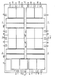
- the present invention provides an integrated circuit for implementing active filters without external components, characterized in that it comprises 16, 8 or 4 amplifying modules, two resistive matrices and a bias circuit, which, with amplifying modules is placed along a first column separated by a resistive matrix from adjacent columns of amplifiers, in turn possibly separated by another resistive matrix from the last column of amplifying modules.
- Fig. 1 The main parts of the integrated circuit are shown in Fig. 1. They consist of 16 amplifying modules, denoted by Al, A2,...A16, programmable both as integrators and as actual broad-band operational amplifiers, of a bias circuit, denoted by CP, suited to feed with bias currents all the amplifying modules, and of two resistive matrices, denoted by MR1 and MR2, consisting of a plurality of equal resistive elements, by which resistive dividers for interconnecting the various amplifying modules can be made.
- the Figure emphasizes the absolute symmetry of the arrangement of amplifying modules and resistive matrices with respect to a vertical median line a-a. This characteristic facilitates programming flexibility of the desired system function. In fact, the suitable choice of the arrangement, as well as of the number of amplifying modules, places each matrix adjacent to eight out of the 16 present modules. As a consequence, connecting lines to be made according to the programmation demanded by the customer do not present particular topological problems.
- Either part of the circuit can be still taken as symmetrical with respect to a median vertical line, b-b or c-c, coincident with a ground electrical line. At its sides there can be found first the resistive matrix elements and then four amplifying modules per side. This arrangement proves particularly advantageous, since a lot of the resistive dividers necessary in a circuit of active "R type filter" have a grounded terminal.
- the ground line is implemented at the first metal level and disposes of different points of contact with the second programmable metal level.
- both parts of the circuit can be taken as symmetrical with respect to a horizontal median line d-d, coincident with a plurality of horizontal metal trunks of the first fixed level. These trunks are used to interconnect a number of pads 1,2...,20 with the amplifying modules and to interconnect the two circuit parts symmetrical with respect to vertical line a-a, the pads meaning little metal regions of the chip used for attaching wires.
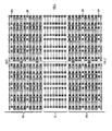
- Fig. 2 shows a detail of. the central zone of a resistive matrix. It consists of 8 columns by 88 rows of modular resistive elements ER horizontally arranged and separated every fourth row by a row SM of 8 metal trunks. The latter trunks are basically usable for connecting the terminals of the various resistors to amplifying modules, to other resistors or to ground. Of course, the desired resistive values are obtained by arranging in series or in parallel a plurality of resistive elements ER.
- Each resistive matrix is traversed in the horizontal median zone by 64 metal trunks SL, horizontally arranged according to a matrix of 8 rows by 8 columns.
- the resistive elements and metal trunks are sized thus as to allow the passage of two vertical metal lines of the programmable second level. They result suitably spaced from each other and each one from the terminals of resistive elements and trunks, according to the standards of the technological method adopted. Based on the desired programmation of the second metal level, the suitable connections with the terminals of resistive elements and trunks can thus be established.
- Said modules can be programmed according to the customer's design through a second metal level so as to make them act, within the filter to be implemented, as actual integrators or as input or output buffers.
- each amplifying module is traversed by electrical lines LP1, LP2, supplying bias currents,and is always connected to power-supply lines Vcc and Vee.
- the module is equipped with points of access to the second metal level, PI and P2, which allow its connection to bias lines LP1 and LP2, according to the filter design required by the customer.
- Each module provided that it is not connected to bias lines, remains inactive and even if fed, doesn't dissipate energy.
- P3 and P4 denote points of access to the second metal level.
- Ou, +In and -In denote respectively access points connected to the output and to the non-inverting and inverting inputs of ' the amplifying module. Output and inverting input are brought closer so as to make their connection easier in case buffer configuration is desired.
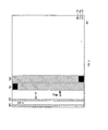
- Fig. 4 shows lines Vee and Vcc distributing power-supply currents to amplifying modules and bias circuit.
- Each line consists in a wide metal routing which horizontally follows the upper or lower boundary of the modules and matrices and in vertical lines for the connection with all the active blocks, according to a comb structure.
- Fig. 5 shows the ground line GND, connected to pad 12, and lines LP1 and LP2 distributing bias currents.
- the ground line consists of a wide horizontal metal routing and of vertical branches traversing the resistive matrices. One of them arrives at bias circuit CP.
- CP is positioned so as to meet three main requirements:
- bias circuit CP in the upper left corner, near pads 1 and 2 and ground line traversing the left resistive matrix, whereto it is connected by a short line trunk.
- Two vertical lines start from the bias circuit directly accessing the first column of the amplifying modules on the left and two horizontal lines follow the upper side. Wherefrom, in suitable position, three pairs of vertical lines are derived for the other three columns of amplifying modules. As already mentioned, the connections between vertical bias lines and amplifying modules are established by means of small jumps implemented at the second metal level, according to the design demanded by the customer.
- Comb lines for power-supply, ground and bias are, however, non-programmable fixed parts of the circuit, that is why they are implemented by using both metal levels.
- All the pads left unused for power-supply, ground or bias- circuit programming, i.e. 3-7, 9, 10, 13-20, are available as- input and output terminals for carrying out the required system functions.
- a number of lines are present which from the pads of the right and left sides, passing into the horizontal median zone, access the closest resistive matrix.
- the lines present on the upper and lower side directly access the vertices of the closest resistive matrix by short and suitable jumps of two metal levels for power-supply, bias and ground.
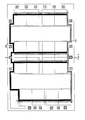
- Fig. 6 shows an integrated circuit comprising only 8 amplifying modules Al,...,A8, an only resistive matrix MR1 and a bias circuit CP.
- Fig. 7 shows a further integrated circuit comprising just 4 amplifying modules A1,...A4, a resistive matrix MR1 of halved size and bias circuit CP. Also in this case the reference numbers of the pads with functions analogous to those of the preceding integrated circuits have been maintained.
Landscapes
- Semiconductor Integrated Circuits (AREA)
- Networks Using Active Elements (AREA)
- Design And Manufacture Of Integrated Circuits (AREA)
- Amplifiers (AREA)
Applications Claiming Priority (2)
| Application Number | Priority Date | Filing Date | Title |
|---|---|---|---|
| IT5325286U | 1986-04-10 | ||
| IT8653252U IT207527Z2 (it) | 1986-04-10 | 1986-04-10 | Circuito integrato per la realizzazione di filtri attivi senza componenti esterni |
Publications (2)
| Publication Number | Publication Date |
|---|---|
| EP0241871A2 true EP0241871A2 (de) | 1987-10-21 |
| EP0241871A3 EP0241871A3 (de) | 1989-03-22 |
Family
ID=11281233
Family Applications (1)
| Application Number | Title | Priority Date | Filing Date |
|---|---|---|---|
| EP87105291A Withdrawn EP0241871A3 (de) | 1986-04-10 | 1987-04-09 | Integrierte Schaltung zur Verwirklichung von aktiven Filtern ohne äusserliche Komponenten |
Country Status (6)
| Country | Link |
|---|---|
| US (1) | US4808947A (de) |
| EP (1) | EP0241871A3 (de) |
| JP (1) | JPS62243411A (de) |
| CA (1) | CA1261073A (de) |
| DE (1) | DE241871T1 (de) |
| IT (1) | IT207527Z2 (de) |
Families Citing this family (1)
| Publication number | Priority date | Publication date | Assignee | Title |
|---|---|---|---|---|
| DE502004008436D1 (de) | 2003-03-01 | 2008-12-24 | Ks Kolbenschmidt Gmbh | Herstellungsverfahren für einen Kühlkanalkolben mit umformbarem Bund |
Family Cites Families (1)
| Publication number | Priority date | Publication date | Assignee | Title |
|---|---|---|---|---|
| US4641108A (en) * | 1985-10-16 | 1987-02-03 | Raytheon Company | Configurable analog integrated circuit |
-
1986
- 1986-04-10 IT IT8653252U patent/IT207527Z2/it active
-
1987
- 1987-04-03 CA CA000533842A patent/CA1261073A/en not_active Expired
- 1987-04-06 JP JP62083138A patent/JPS62243411A/ja active Granted
- 1987-04-08 US US07/035,984 patent/US4808947A/en not_active Expired - Fee Related
- 1987-04-09 DE DE198787105291T patent/DE241871T1/de active Pending
- 1987-04-09 EP EP87105291A patent/EP0241871A3/de not_active Withdrawn
Non-Patent Citations (4)
| Title |
|---|
| ELECTRONIC DESIGN, vol. 28, no. 4, 15th February 1980, pages 63-65, St Rochelle Park, US; M. GROSSMAN: "Dedicated LSI chips come out as costs drop" * |
| PROCEEDINGS OF THE NATIONAL ELECTRONICS CONFERENCE, vol. 32, October 1978, pages 233-238, Oak Brook, US; D.R. CURTIS et al.: "Design considerations for a bipolar semi-custom chip" * |
| THE 2ND INTERNATIONAL CONFERENCE ON SEMI-CUSTOM ICS, pages 70-83; P.R. IRISSOU: "Combining linear and digital functions on a single bipolar, C-MOS or ULA chip" * |
| WESCON TECHNICAL PAPERS, 30th October - 2nd November 1984, pages 1-6, Anaheim, California, Los Angeles, US; G. KELSON: "Advanced design automation techniques for analog VLSI" * |
Also Published As
| Publication number | Publication date |
|---|---|
| US4808947A (en) | 1989-02-28 |
| JPS62243411A (ja) | 1987-10-23 |
| DE241871T1 (de) | 1989-07-13 |
| CA1261073A (en) | 1989-09-26 |
| IT8653252V0 (it) | 1986-04-10 |
| EP0241871A3 (de) | 1989-03-22 |
| JPH0548956B2 (de) | 1993-07-22 |
| IT207527Z2 (it) | 1988-01-25 |
Similar Documents
| Publication | Publication Date | Title |
|---|---|---|
| US4472765A (en) | Circuit structure | |
| DE69016462T2 (de) | Elektronisches system mit änderungsfähigkeit durch direktes schreiben. | |
| US4603377A (en) | Main distributing frame board for an electronic switching system | |
| JP3786455B2 (ja) | 制御装置用のモジュール形端子ブロック装置 | |
| DE68921312T2 (de) | Aufbau für selbstleitweglenkendes Paketvermittlungsnetz. | |
| US5432708A (en) | Multichip module integrated circuit device having maximum input/output capability | |
| DE3780915T2 (de) | Biegsamer film-chiptraeger mit entkopplungskondensatoren. | |
| US4514786A (en) | Integrated-circuit support device employed in a system for selecting high-reliability integrated circuits | |
| JPS60254762A (ja) | 半導体素子のパツケ−ジ | |
| US6570429B1 (en) | Method and apparatus for providing a clock signal to a semiconductor chip | |
| US4906987A (en) | Printed circuit board system and method | |
| EP0241871A2 (de) | Integrierte Schaltung zur Verwirklichung von aktiven Filtern ohne äusserliche Komponenten | |
| JP2576552B2 (ja) | インバータの素子配列 | |
| US5668389A (en) | Optimized power bus structure | |
| NL8103882A (nl) | Inrichting met onder hoge dichtheid hierin opgenomen geintegreerde schakelingen. | |
| DE60033300T2 (de) | Verfahren und vorrichtung zur mehrkanaligen signalverarbeitung | |
| US5982599A (en) | Input/output electrostatic discharge protection for devices with multiple individual power groups | |
| JPH07249735A (ja) | 半導体素子の並列接続方法 | |
| US3851124A (en) | Crosspoint matrix arrangement for space-division communication switching network | |
| EP0769679A1 (de) | Einbau-Mehrkanalschreiber | |
| JPH023559B2 (de) | ||
| JP2929784B2 (ja) | 半導体集積回路装置 | |
| US6646475B2 (en) | On-chip power supply with optimized electromagnetic compatibility | |
| EP0587962A1 (de) | Verfahren und Schaltung zur Ausführung einer Impedanz, insbesondere für telefonische Gleichstrom-Anwendungen | |
| US5815728A (en) | Processor array |
Legal Events
| Date | Code | Title | Description |
|---|---|---|---|
| PUAI | Public reference made under article 153(3) epc to a published international application that has entered the european phase |
Free format text: ORIGINAL CODE: 0009012 |
|
| AK | Designated contracting states |
Kind code of ref document: A2 Designated state(s): DE FR GB NL SE |
|
| PUAL | Search report despatched |
Free format text: ORIGINAL CODE: 0009013 |
|
| AK | Designated contracting states |
Kind code of ref document: A3 Designated state(s): DE FR GB NL SE |
|
| EL | Fr: translation of claims filed | ||
| 17P | Request for examination filed |
Effective date: 19890308 |
|
| TCNL | Nl: translation of patent claims filed | ||
| DET | De: translation of patent claims | ||
| 17Q | First examination report despatched |
Effective date: 19910620 |
|
| STAA | Information on the status of an ep patent application or granted ep patent |
Free format text: STATUS: THE APPLICATION IS DEEMED TO BE WITHDRAWN |
|
| 18D | Application deemed to be withdrawn |
Effective date: 19911031 |
|
| RIN1 | Information on inventor provided before grant (corrected) |
Inventor name: GANDINI, MARCO Inventor name: SARTORI, MARIO Inventor name: GAIDANO, ROBERTO |