EP0241266B1 - Elektronische Uhr - Google Patents
Elektronische Uhr Download PDFInfo
- Publication number
- EP0241266B1 EP0241266B1 EP87303014A EP87303014A EP0241266B1 EP 0241266 B1 EP0241266 B1 EP 0241266B1 EP 87303014 A EP87303014 A EP 87303014A EP 87303014 A EP87303014 A EP 87303014A EP 0241266 B1 EP0241266 B1 EP 0241266B1
- Authority
- EP
- European Patent Office
- Prior art keywords
- temperature
- adjusting
- output signal
- temperature gradient
- frequency
- Prior art date
- Legal status (The legal status is an assumption and is not a legal conclusion. Google has not performed a legal analysis and makes no representation as to the accuracy of the status listed.)
- Expired
Links
Images


Classifications
-
- G—PHYSICS
- G04—HOROLOGY
- G04G—ELECTRONIC TIME-PIECES
- G04G3/00—Producing timing pulses
- G04G3/02—Circuits for deriving low frequency timing pulses from pulses of higher frequency
- G04G3/022—Circuits for deriving low frequency timing pulses from pulses of higher frequency the desired number of pulses per unit of time being obtained by adding to or substracting from a pulse train one or more pulses
-
- G—PHYSICS
- G04—HOROLOGY
- G04F—TIME-INTERVAL MEASURING
- G04F5/00—Apparatus for producing preselected time intervals for use as timing standards
- G04F5/04—Apparatus for producing preselected time intervals for use as timing standards using oscillators with electromechanical resonators producing electric oscillations or timing pulses
- G04F5/06—Apparatus for producing preselected time intervals for use as timing standards using oscillators with electromechanical resonators producing electric oscillations or timing pulses using piezoelectric resonators
Definitions
- the present invention relates to electronic watches and particularly, but not exclusively to temperature-compensated electronic watches having a temperature sensitive oscillator constructed in a MOS-IC.
- the electronic watch comprises a quartz oscillator having temperature characteristics, a frequency divider for generating a train of signals having a lower frequency from the oscillating signal of the quartz oscillator, a driver for composing the output signal train of the frequency divider to generate a drive signal, a display unit for displaying the time on the basis of the output signal of the driver, a temperature sensitive oscillator in the vicinity of the quartz oscillator and having its output signal frequency or period varying linearly with the temperature, a temperature gradient adjusting means for logically adjusting the temperature gradient of the output signal frequency or period of the temperature sensitive oscillator, an offset adjusting means for logically adjusting the offset of the temperature characteristics of the output signal frequency or period of the temperature sensitive oscillator, a frequency corrector for temperature compensation of the output of the quartz oscillator on the basis of the temperature data which is prepared from the output signal of the temperature sensitive oscillator by the gradient adjusting means and the offset adjusting means and a controller for using the output signal train of the frequency
- the temperature gradient adjusting means operates with temperature gradient adjusting numerical data only, and without any rough temperature gradient adjusting variable frequency divider interposed between the temperature sensitive oscillator and the temperature gradient adjusting means.
- the present invention also seeks to provide an improved voltage regulator for a temperature sensitive oscillator to optimise the linearity of frequency versus temperature from outside.
- a rough temperature gradient adjusting variable frequency divider is arranged variably to divide the frequency of the output signal of the temperature sensitive oscillator, and the temperature gradient adjusting means is operated at a value which is set by adding a constant numerical value to the temperature gradient adjusting numerical data, so that the temperature gradient adjusting range can be widened without any drop in the temperature gradient adjusting resolution of the temperature sensitive oscillator.
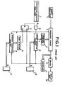
- An electronic watch comprises a quartz oscillator 1 having temperature sensitive characteristics, a frequency divider 2 generating a train of signals having a lower frequency from the oscillating signal of oscillator 1, a driver 3 generating drive signals responsive to the output signal train of the divider 2, and a display unit 20 for displaying the time on the basis of the output of the driver 3.
- Temperature measurement is conducted at constant time intervals by a controller 6.
- an offset adjusting counter 10 and a gradient adjusting counter 8 are set with adjusting numerical data B and A, respectively, from circuits 32 and 31 by the controller 6.
- a latch 11 is set by the controller 6, which provides an input to open an AND gate 12, so that the output signal fs of the temperature sensitive oscillator 7 begins to be input to the offset adjusting counter 10 via the AND gate 12.
- a signal fc from the frequency divider 2 driven by the quartz oscillator 1 is input to the gradient adjusting counter 8.
- letter e designates the number of bits of the offset adjusting counter 10
- letter m designates the number of times of overflows.
- Letter e designates the temperature
- letter fo designates the frequency at 0 ° C
- letter a designates a temperature coefficient.
- Symbol "[ ]” designates the operation to round the numeral to nearest integer.
- the temperature data T is applied to a frequency corrector 5 connected to the frequency divider 2 which supplies the controller 6 and the driver 3 for the display unit 20.
- Temperature compensation in the case of Figure 2 is substantially the same as that in the case of Figure 1, except that the output signal period T s of the oscillator 7 varies linearly with temperature.
- the signal fc is fed to one input of the AND gate 12 instead of the output of the temperature sensitive oscillator 7, whose output ⁇ s is to the gradient adjusting counter 8.
- the temperature data T of this case can be expressed by the following equation: wherein
- letter ro designates the period of the temperature sensitive oscillator 7 at 0 ° C
- letter p designates a temperature coefficient
- the temperature gradient adjustors thus constructed are accompanied by a defect that the temperature gradient adjusting resolution (i.e. 1/A: the reciprocal number of the adjusting numerical data A) degrades the greater the frequency-temperature gradient or the period-temperature gradient of the temperature sensitive oscillator becomes.
- the defect is that such a temperature gradient adjusting range is narrowed as can be used without any drop in the temperature gradient adjusting resolution.
- the temperature gradient adjusting range will be determined in the following by substituting specific numerical values into the equations (1) and (2). If the temperature data T has a temperature dependent term T e, this term can be expressed by the following equation from the equations (1) and (2):
- the upper and lower limits of the value a i.e., the temperature gradient adjusting range will be calculated by substituting an appropriate specific numerical value into the equation (5).
- the gradient adjusting counter 8 is a counter of ten bits
- the adjusting numerical data A takes 10 bits.
- the signal fc to be used has 2048Hz of the frequency divider.
- the adjusting numerical data A exceeds 1024 so that it cannot make an adjustment. In case the temperature gradient a is not larger than 40 (Hz/ ° C), the adjusting numerical data A becomes equal to or smaller than 511 so that the temperature gradient adjusting resolution exceeds 1/512.
- the adjusting numerical information A exceeds 1024 to make the adjustment impossible, if the temperature gradient p becomes equal to or smaller than 4.77 ( ⁇ sec/°C), and becomes equal to or smaller than 511 to make the adjusting resolution equal to or more than 1/512, if the gradient p exceeds 9.54 (ysec/ ° C).
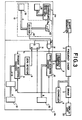
- a rough temperature gradient adjusting variable frequency divider 13 is inserted between the AND gate 12 and the temperature sensitive oscillator 7 of Figure 1, and the gradient adjusting counter 8 is operated at a value which is set by adding a constant numerical value D by circuit 34 to the adjusting numerical data A from circuit 31.
- These alterations are represented by blocks 4a and 4b, respectively.
- a variable frequency divider 13 is added to the circuit of Figure 2, and the gradient adjusting counter 8 is operated at a value which is set by adding the numerical value D to tn Q adjusting numerical data A.
- the constant numerical value D to be added to the temperature gradient adjusting numerical data A is the maximum of data A plus 1.
- the frequency divider 13 comprises a circuit 33 whose output C is three bit rough temperature gradient adjusting numerical data. This data is supplied to a selector 40 whose other input is the output of a frequency divider 50 whose input is either fs signals or us signals. The output of the selector 40 is either fs1 signals or TS 1 signals. These alterations are represented by blocks 4a and 4c, respectively.
- the division ratio of the divider 13 is an nth power of 2, where n is an integer.
- Letter D designates a constant numerical value to be added to the temperature gradient adjusting numerical data A
- letter C designates data concerning how many flip-flops are to be added for dividing the output signal of the temperature sensitive oscillator 7 into one half.
- the added numerical value D need not be added to the adjusting numerical value A but may take any construction if the output signal of the temperature sensitive oscillator never fails to be input to the offset adjusting counter for a constant period of time having no relation to the adjusting numerical value A.
- the variable frequency dividing data C need not be constructed to specify how many flip-flops to be added, as shown in Figure 3, but may take any construction if the frequency of the output signal of the temperature sensitive oscillator is variably divided.
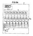
- the temperature sensitive oscillator 7 outputs a signal at a frequency fs varying linearly with the temperature, and this output signal frequency fs is input to the frequency divider 50.
- the selector 40 is composed of eight transmission gates and a decoder, and one of the eight transmission gates is selectively turned on at the numerical value which is set by the rough temperature gradient adjusting numerical data C of three bits.
- the resultant output signal fs1 is expressed by the following equation:
- the fine temperature gradient numerical data A ( Figure 5B) is composed of ten bits and takes a value of 0 to 1023.
- the adjusting numerical value A is input to the lower ten bits of the input D of the gradient adjusting presettable down counter 8 (block 4b) composed of eleven bits. Because the highest bit of the input D is fixed at "1", the value to be preset in the gradient adjusting counter 8 is the adjusting numerical A + 1.
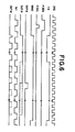
- An output signal WIND ( Figure 6) from the controller 6 and an output signal 2KQ ( Figure 6) from the frequency divider 2 are input to an AND gate 14 ( Figure 5B), the output of which is input to the gradient adjusting counter 8 as 0.
- the output Q of eleven bits of the gradient adjusting counter 8 is input to the zero detector 9, the output (OUT9, Figure 6) of which is input to the reset of the latch 11 ( Figure 5B).
- This latch 11 has its set fed with a signal which is prepared by inverting an output signal 1Q ( Figure 6) of 1 Hz from the frequency divider 2 by an inverter 15 ( Figure 5B).
- the output signal (OUT11, Figure 6) of the latch 11 ( Figure 5B) and the output signal fs1 are input to the AND gate 12, whose output (OUT12, Figure 6) is input to the offset adjusting presettable counter 10 as 0 ( Figure 5B).
- the offset adjusting numerical data B is composed of ten bits and takes a value of 0 to 1023.
- the adjusting numerical value B is input to the D of the offset adjusting counter 10 composed of ten bits.
- the ten bit output Q of the offset adjusting counter 10 is the temperature data T and is input to the frequency corrector 5.
- an output signal P.SEN ( Figure 6) is first output from the controller 6 to the counters 8 and 10 ( Figure 5B) so that the gradient adjusting counter and the offset adjusting counter are set in their preset states.
- An output signal P.SCL is thereafter output from the controller 6 to preset the gradient adjusting counter and the offset adjusting counter with the adjusting numerical values A and B, respectively.
- the OUT11 signal rises upon the fall of the 1Q signal and the signal fs1 begins to be input to the 0 of the offset adjusting counter 10 via the AND gate 12.
- WIND rises
- 2KQ begins to be input to the 0 of the gradient adjusting counter 8 via the AND gate 14.
- the temperature sensitive oscillator 7 has its output period T s varying linearly with temperature.
- the output signal is1 of the selector 40 is expressed by the following equation:
- the adjusting numerical values A and B are preset into the gradient adjusting counter 8 and the offset adjusting counter 10, respectively, by the signals P.SEN and P.SCL.
- the signal OUT11 rises so that the signal 2KQ begins to be input to the 0 of the offset adjusting counter 10 via the AND gate 12.
- the output signal rs1 begins to be input to the 0 of the gradient adjusting counter 8 via the AND gate 14 in response to the rise of the signal WIND.
- the zero detector 9 detects the zero and the signal OUT9 rises.
- the signal OUT11 falls, closing the AND gate 12 and cutting off the signal 2KQ from the counter 10.
- the resultant temperature data T can be expressed by the following equation: wherein
- the temperature gradient adjusting range in the case of the present invention can be deduced from the following. If the temperature data T has a term T edepending upon the temperature, this term T e can be expressed by the following equation from the equations (10) and (2):
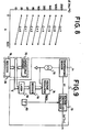
- the adjustable range of the temperature gradient a can be calculated from the equation (12) so that the following very wide gradient adjusting range can be achieved, as shown in Figure 8:
- the adjusting numerical value A can make an error of 0.5 at the maximum for adjustment, because it is integral.
- the influence to be given to the temperature information T e by the error of 0.5 and the temperature gradient adjusting numerical value A is moderated by the value D.
- the temperature sensitive oscillator 7 ( Figure 9) has an externally controllable constant voltage circuit and receives numerical information E from circuit 35 for fine regulation of a constant voltage value.
- a temperature sensor 71 is composed of an IC sensor which is fabricated on an LSI chips.
- a constant current circuit 72 improves linearity of output voltage versus temperature of the temperature sensor 71.
- the output frequency of a voltage controlled oscillator 73 is influenced by an output V T of the temperature sensor 71, so that temperature change is converted into a frequency change.
- the voltage controlled oscillator 73 is supplied with a constant regulated supply voltage V REG from a voltage regulator 74.
- An optimum numerical correcting value E is input to the voltage regulator 74 through a latch 78 and a decoder 79 in order to obtain a wide linear range of the frequency fs versus the temperature.
- the numerical value E is set in a register 76 by monitoring a test terminal 80 until a desired supply voltage V REG is obtained with a particular correcting value E from the circuit 35. Then after fixing that optimum correcting value E, it is stored semi-permanently in a non-volatile memory 75.
- the voltage regulator 74 ( Figure 10) includes voltage dividing resistors 92, analog switches 91 and a constant voltage generator 90 for generating the constant voltage V REG to be applied to the voltage controlled oscillator 73.
- the constant voltage value is monitored by a test terminal 80 so that a correcting value can be input to the register 76 if it is offset from the target value.
- the correcting value input to that register is transferred through the latch 78 which is a half latch, to the decoder 79, which in turn determines in accordance with the correcting value which of the analog switches 91 is to be turned ON and which OFF.
- the divided voltages generated by the group of voltage dividing resistors 92 are input to an OP amplifier 93 in the constant voltage generator 90 where they are compared with a reference voltage generated from a reference voltage generator 94 to vary the gate voltage of a MOS resistor 95.
- the constant voltage V REG is varied. If this constant voltage V REG is not satisfactory, the aforementioned operations are repeated by inputting again a new correcting value.
- the correcting value is written in the non-volatile memory 75. If the correcting value is then read out, if necessary, from the non-volatile memory and latched in the half latch 78, an optimum constant voltage is obtained as the value V REG .
- the temperature gradient adjusting range can be widened without any drop in the temperature gradient adjusting resolution. More specifically, it is possible to adjust even the larger dispersions of the temperature gradient of the temperature sensitive oscillator which is made monolithic in the MOS-IC. Moreover, the linearity of frequency versus temperature is optimised by external adjustable voltage regulator. This makes it easy to design the temperature sensitive oscillator and to perform the process control for the IC fabrication while reducing the defect rate and production cost.
Landscapes
- Physics & Mathematics (AREA)
- General Physics & Mathematics (AREA)
- Electric Clocks (AREA)
- Oscillators With Electromechanical Resonators (AREA)
Claims (5)
Applications Claiming Priority (4)
| Application Number | Priority Date | Filing Date | Title |
|---|---|---|---|
| JP61080720A JP2510415B2 (ja) | 1986-04-08 | 1986-04-08 | 電子時計 |
| JP80720/86 | 1986-04-08 | ||
| JP83027/86 | 1986-04-10 | ||
| JP8302786A JPS62238486A (ja) | 1986-04-10 | 1986-04-10 | 電子時計における定電圧の調整方法 |
Publications (3)
| Publication Number | Publication Date |
|---|---|
| EP0241266A2 EP0241266A2 (de) | 1987-10-14 |
| EP0241266A3 EP0241266A3 (en) | 1988-03-30 |
| EP0241266B1 true EP0241266B1 (de) | 1990-11-14 |
Family
ID=26421693
Family Applications (1)
| Application Number | Title | Priority Date | Filing Date |
|---|---|---|---|
| EP87303014A Expired EP0241266B1 (de) | 1986-04-08 | 1987-04-07 | Elektronische Uhr |
Country Status (3)
| Country | Link |
|---|---|
| US (1) | US4737944A (de) |
| EP (1) | EP0241266B1 (de) |
| DE (1) | DE3766143D1 (de) |
Families Citing this family (5)
| Publication number | Priority date | Publication date | Assignee | Title |
|---|---|---|---|---|
| JPH07244540A (ja) * | 1994-03-03 | 1995-09-19 | Fujitsu Ltd | 高精度時計装置 |
| US6086244A (en) * | 1997-03-20 | 2000-07-11 | Stmicroelectronics, Inc. | Low power, cost effective, temperature compensated, real time clock and method of clocking systems |
| US20090129208A1 (en) * | 2009-01-28 | 2009-05-21 | Weiss Kenneth P | Apparatus, system and method for keeping time |
| JP6686329B2 (ja) | 2015-08-28 | 2020-04-22 | セイコーエプソン株式会社 | 発振回路、電子機器及び移動体 |
| JP6728598B2 (ja) | 2015-08-28 | 2020-07-22 | セイコーエプソン株式会社 | 発振回路、電子機器及び移動体 |
Family Cites Families (5)
| Publication number | Priority date | Publication date | Assignee | Title |
|---|---|---|---|---|
| JPS5633587A (en) * | 1979-08-24 | 1981-04-04 | Casio Comput Co Ltd | Electronic watch |
| CH643106B (fr) * | 1980-11-26 | Suisse Horlogerie | Garde-temps comprenant une chaine de diviseurs au rapport de division ajustable. | |
| US4453834A (en) * | 1981-07-03 | 1984-06-12 | Citizen Watch Company Limited | Electronic timepiece with temperature compensation |
| DE3135228C2 (de) * | 1981-09-05 | 1984-12-13 | Vdo Adolf Schindling Ag, 6000 Frankfurt | Schaltungsanordnung zum Abgleich einer Pulsfrequenz einer quarzgesteuerten Uhr |
| US4473303A (en) * | 1982-02-19 | 1984-09-25 | Citizen Watch Company Limited | Electronic timepiece |
-
1987
- 1987-04-06 US US07/035,093 patent/US4737944A/en not_active Expired - Fee Related
- 1987-04-07 EP EP87303014A patent/EP0241266B1/de not_active Expired
- 1987-04-07 DE DE8787303014T patent/DE3766143D1/de not_active Expired - Fee Related
Also Published As
| Publication number | Publication date |
|---|---|
| US4737944A (en) | 1988-04-12 |
| DE3766143D1 (de) | 1990-12-20 |
| EP0241266A3 (en) | 1988-03-30 |
| EP0241266A2 (de) | 1987-10-14 |
Similar Documents
| Publication | Publication Date | Title |
|---|---|---|
| EP0181047B1 (de) | Verzögerungssteuerungsschaltung und Verfahren zur Steuerung der Verzögerungen in einem Halbleiterelement | |
| US7026850B2 (en) | Programmable self-calibrating vernier and method | |
| US4899117A (en) | High accuracy frequency standard and clock system | |
| US5745011A (en) | Data recovery phase locked loop | |
| US20120286831A1 (en) | Circuit and method for generating a clock signal | |
| US5087870A (en) | Constant power circuit | |
| US4910473A (en) | Digitally temperature-compensated oscillator | |
| US7154351B2 (en) | Approximate n-th order function generating device and temperature compensation crystal oscillation circuit | |
| US5525936A (en) | Temperature-compensated oscillator circuit | |
| EP0241266B1 (de) | Elektronische Uhr | |
| EP0104770B1 (de) | Temperaturabhängiger Spannungsgeneratorkreis | |
| EP0166706B1 (de) | Verfahren zur Messung von Kapazitäten, insbesondere niedrigen Kapazitäten | |
| US4563748A (en) | Temperature measuring system | |
| US4465379A (en) | Temperature detector circuit for timepiece | |
| US6729755B1 (en) | Low power, cost effective, temperature compensated real time clock and method of clocking systems | |
| US4300224A (en) | Electronic timepiece | |
| US4037399A (en) | Electronic timepiece battery potential detecting circuitry | |
| Bloch et al. | The microcomputer compensated crystal oscillator (MCXO) | |
| US4142360A (en) | Electronic timepiece | |
| EP0241253B1 (de) | Elektronische Uhr | |
| US4730286A (en) | Circuit and method for correcting the rate of an electronic timepiece | |
| JP2510415B2 (ja) | 電子時計 | |
| KR100319970B1 (ko) | 루비듐원자 주파수표준기의 성능향상을 위한 장치 및평가방법 | |
| DE3014093A1 (de) | Quarzoszillator mit hoher frequenzkonstanz und geringem strombedarf fuer einfache serienfertigung | |
| JPS6140586A (ja) | 電子時計 |
Legal Events
| Date | Code | Title | Description |
|---|---|---|---|
| PUAI | Public reference made under article 153(3) epc to a published international application that has entered the european phase |
Free format text: ORIGINAL CODE: 0009012 |
|
| AK | Designated contracting states |
Kind code of ref document: A2 Designated state(s): CH DE GB LI |
|
| PUAL | Search report despatched |
Free format text: ORIGINAL CODE: 0009013 |
|
| AK | Designated contracting states |
Kind code of ref document: A3 Designated state(s): CH DE GB LI |
|
| 17P | Request for examination filed |
Effective date: 19880825 |
|
| R17P | Request for examination filed (corrected) |
Effective date: 19880825 |
|
| 17Q | First examination report despatched |
Effective date: 19900212 |
|
| GRAA | (expected) grant |
Free format text: ORIGINAL CODE: 0009210 |
|
| AK | Designated contracting states |
Kind code of ref document: B1 Designated state(s): CH DE GB LI |
|
| REF | Corresponds to: |
Ref document number: 3766143 Country of ref document: DE Date of ref document: 19901220 |
|
| PGFP | Annual fee paid to national office [announced via postgrant information from national office to epo] |
Ref country code: GB Payment date: 19910327 Year of fee payment: 5 |
|
| PGFP | Annual fee paid to national office [announced via postgrant information from national office to epo] |
Ref country code: DE Payment date: 19910411 Year of fee payment: 5 |
|
| PLBE | No opposition filed within time limit |
Free format text: ORIGINAL CODE: 0009261 |
|
| STAA | Information on the status of an ep patent application or granted ep patent |
Free format text: STATUS: NO OPPOSITION FILED WITHIN TIME LIMIT |
|
| 26N | No opposition filed | ||
| PG25 | Lapsed in a contracting state [announced via postgrant information from national office to epo] |
Ref country code: GB Effective date: 19920407 |
|
| GBPC | Gb: european patent ceased through non-payment of renewal fee | ||
| PG25 | Lapsed in a contracting state [announced via postgrant information from national office to epo] |
Ref country code: DE Effective date: 19930101 |
|
| PGFP | Annual fee paid to national office [announced via postgrant information from national office to epo] |
Ref country code: CH Payment date: 20060413 Year of fee payment: 20 |
|
| REG | Reference to a national code |
Ref country code: CH Ref legal event code: PL |