EP0240135B1 - Bloch line memory device and method for operating same - Google Patents
Bloch line memory device and method for operating same Download PDFInfo
- Publication number
- EP0240135B1 EP0240135B1 EP87301591A EP87301591A EP0240135B1 EP 0240135 B1 EP0240135 B1 EP 0240135B1 EP 87301591 A EP87301591 A EP 87301591A EP 87301591 A EP87301591 A EP 87301591A EP 0240135 B1 EP0240135 B1 EP 0240135B1
- Authority
- EP
- European Patent Office
- Prior art keywords
- magnetic
- domain
- bloch
- stripe
- magnetic domain
- Prior art date
- Legal status (The legal status is an assumption and is not a legal conclusion. Google has not performed a legal analysis and makes no representation as to the accuracy of the status listed.)
- Expired - Lifetime
Links
Images


Classifications
-
- G—PHYSICS
- G11—INFORMATION STORAGE
- G11C—STATIC STORES
- G11C19/00—Digital stores in which the information is moved stepwise, e.g. shift registers
- G11C19/02—Digital stores in which the information is moved stepwise, e.g. shift registers using magnetic elements
- G11C19/08—Digital stores in which the information is moved stepwise, e.g. shift registers using magnetic elements using thin films in plane structure
- G11C19/0875—Organisation of a plurality of magnetic shift registers
- G11C19/0883—Means for switching magnetic domains from one path into another path, i.e. transfer switches, swap gates or decoders
-
- G—PHYSICS
- G11—INFORMATION STORAGE
- G11C—STATIC STORES
- G11C19/00—Digital stores in which the information is moved stepwise, e.g. shift registers
- G11C19/02—Digital stores in which the information is moved stepwise, e.g. shift registers using magnetic elements
- G11C19/08—Digital stores in which the information is moved stepwise, e.g. shift registers using magnetic elements using thin films in plane structure
- G11C19/0858—Generating, replicating or annihilating magnetic domains (also comprising different types of magnetic domains, e.g. "Hard Bubbles")
-
- G—PHYSICS
- G11—INFORMATION STORAGE
- G11C—STATIC STORES
- G11C19/00—Digital stores in which the information is moved stepwise, e.g. shift registers
- G11C19/02—Digital stores in which the information is moved stepwise, e.g. shift registers using magnetic elements
- G11C19/08—Digital stores in which the information is moved stepwise, e.g. shift registers using magnetic elements using thin films in plane structure
- G11C19/0866—Detecting magnetic domains
Definitions
- This invention relates to a Bloch line memory device and a method for operating same and in particular to a Bloch line memory device and a method for operating same, which are suitable for obtaining a good read-out margin and practical.
- a magnetic garnet film is used as a memory medium film as in a magnetic bubble memory device.
- their memory methods are considerably different. That is, in a Bloch line memory the presence and the absence of a vertical Bloch line pair existing in the wall around a stripe magnetic domain obtained by stretching a bubble correspond to "1" and "0", respectively, while in a prior art magnetic bubble memory the presence and the absence of a bubble correspond to "1" and "0" in data.
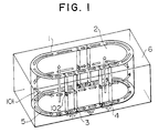
- Fig. 1 indicates this aspect.
- the arrow directed upward in a stripe magnetic domain 2 shows the direction of magnetization
- arrows 101 on the center line of the wall 1 show the direction of magnetization located at the wall center
- arrows 102 perpendicular to the wall 1 at the center line show the direction of magnetization at the center of the vertical Bloch line (hereinbelow called merely Bloch line).
- portions, where a pair of Bloch lines exist correspond to "1" in data and portions, where no Bloch lines exist, correspond to "0".
- the Bloch line used as information carrier is a microstructure of the domain wall existing in the wall 1 surrounding the magnetic domain.
- the Bloch line can exist stably in the domain wall and propagate freely along the domain wall. Consequently, when a number of stripe magnetic domains are arranged at their predetermined positions and Bloch lines are made to exist in the domain wall, they behave just as bubbles propagating in a minor loop of a magnetic bubble memory. For this reason a Bloch line memory is a shift resistor type memory similarly to a magnetic bubble memory.
- Bloch line The existence of the Bloch line is known since long ago and it is verified by experiments and their analysis that the mobility of the magnetic domain is reduced by the existence of the Bloch line. Consequently, for the magnetic bubble memory, for which the magnetic domain should be shifted, the bubble domain containing Bloch lines is called hard bubble and it has been tried to prevent its generation. To the contrary, for the Bloch line memory device, the existence of this Bloch line is positively utilized.
- the physical size of the Bloch line is about 1/10 of the width of the stripe magnetic domain, where the Bloch line exists, and a number of Bloch lines can exist in one stripe magnetic domain.
- a number of Bloch lines can exist in one stripe magnetic domain.
- the physical size of the Bloch line is about 1/10 of the width of the stripe magnetic domain, where the Bloch line exists, and a number of Bloch lines can exist in one stripe magnetic domain.
- a garnet film having stripe magnetic domains 1 ⁇ m wide developed for a magnetic bubble memory it is possible to make about 5 x 10⁶ Bloch lines exist per 1 cm3. Therefore, in the case where 2 Bloch lines are paired in the information medium, it is possible to realize a memory of 256 M bit/cm2.
- Bloch line memory device can have a large memory capacity, apart from the fact that the size is extremely small. It is due to the fact that in the Bloch line memory the magnetic field in the vertical direction is used for the propagation of information, while in the magnetic bubble memory information carriers are propagated by rotating an in-plane field. For this reason there is a high possibility that the propagation pattern is simplified in a plane, what acts so as to make it easier to increase the density for this type of memory elements.
- the write-in operation is effected basically by making electric current flow through a conductor disposed at the proximity of one stripe domain head so that a local magnetic field is generated there and reversing the magnetization in the domain wall. That is, it can be thought that the direction of magnetization indicated by "0" in Fig. 1 is reversed so that it is in accordance with the direction of magnetization in the "1" domain.
- Bloch lines are produced in this way. Further two Bloch lines are always paired. Consequently the Bloch line memory is constituted by making one pair of Bloch lines correspond to one information.
- the read-out of information is effected, after having transformed the presence or absence of the Bloch line into the presence or absence of the bubble domain.
- the transformation of the Bloch line into the bubble domain is effected by the method described by Konishi in an article published in IEEE Trans. Mag. 19 , No. 5 (1983) p. 1838 - p. 1840 and p. 1841 - p. 1843. That is, when a pair of Bloch lines exist, the direction of magnetization in the domain wall is reversed at the pair of Bloch lines as a border, as indicated in Fig. 1. When a pair of Bloch lines arrive at the stripe magnetic domain head, variations in this magnetization structure give rise to variations in chopping properties.
- Fig. 2 is a top view of the element indicated in Fig. 1, in which also the direction of magnetization seen from above is indicated by arrows.
- the presence or absence of the Bloch lines can be transformed into the presence or absence of the bubble.
- Bloch line memory It is possible to realize a Bloch line memory by forming a write-in, a memory and a read-out function portion described above in one element.
- Fig. 3A indicates a case where a pair of Bloch lines 4 arrive at the head portion of a stripe magnetic domain 2 and on the other hand Fig. 3B indicates a case where there are no pair of Bloch lines. In the two states, comparing the directions of the magnetizations 5 of the domain wall 1, it can be seen that the two are same.
- the magnetization of the domain wall varies, depending on whether a pair of Bloch lines exist or not, but the magnetization doesn't vary, depending on whether a pair of Bloch lines exist or not. This reason is that the magnetization reversed by one Bloch line is reversed again by the other Bloch line so that the direction of the magnetization returns finally to the initial one. For this reason, since the direction of the magnetizations 5 doesn't vary depending on the presence or absence of the pair of Bloch lines only by the prior art method, it can be understood that its presence or absence cannot be transformed into the presence or absence of the magnetic bubble domain.
- JP-A-59-101092 As measures for resolving this problem a method is disclosed in JP-A-59-101092.
- electric current is made to flow through a conductor superposed on the chopping conductor so that the position of the pair of Bloch lines is held and reading-out is carried out by effecting the chopping operation between the pair of Bloch lines.
- the presence or absence of the pair of Bloch lines can be transformed into the presence or absence of the bubble domain and thus the reading-out according to the prior art techniques is realized.
- EP-A-106358 also discloses a magnetic memory in which information is stored by the use of vertical Bloch lines in a stripe magnetic domain.
- the presence or absence of the Bloch line pairs dictates the type of information stored in the memory.
- the information is read out by chopping the end of the preselected stripe domain. This is done by supplying a local in-plane magnetic field to the end of the stripe domain head such that the pair of Bloch lines are split.
- the head of the stripe can then be chopped to form a bubble by a field generated by a chopping conduction, which is located between the Bloch lines.
- the present invention seeks to provide a practical Bloch line memory device, in which a pair of Bloch lines represent one bit information and a method for operating same.
- the present invention therefore provides a Bloch line memory device comprising: a magnetic medium film; means for holding a stripe magnetic domain at a desired region of the magnetic medium film, the stripe magnetic domain including at least one pair of Bloch lines; means for shifting said pair of Bloch lines towards a head portion of said stripe magnetic domain; means disposed at the proximity of the head portion of said stripe magnetic domain for chopping the stripe magnetic domain by bringing upper and lower sides of a domain wall of the stripe magnetic domain closer to each other; and means for applying an in-plane magnetic field (HC) to the magnetic medium film; wherein said device further comprises means for stretching said head portion of the strip magnetic domain in a direction substantially parallel to the magnetic medium film by applying a magnetic force ( HB) in a direction substantially opposite to a vertical bias magnetic field (H B ) perpendicular to the magnetic medium film, and for simultaneously splitting the pair of Bloch lines by applying the in-plane magnetic field (H C ) provided by the means for applying the in-plane magnetic field; and
- the direction of this in-plane magnetic field may be determined so that it is also opposite to the direction, along which the stripe magnetic domain stretches (Y axis direction).
- a force tending to make the magnetic energy small acts on the region surrounded by the pair of Bloch lines. Consequentially the region is enlarged by this force and the distance bewtween the two Bloch lines forming the pair of Bloch lines increases.
- one of the Bloch lines becomes more distant from the head portion of the stripe magnetic domain and the other is held stably at the head portion of the stripe magnetic domain.
- stripe magnetic domain chopping means disposed at the proximity of the head portion of the stripe domain chops the stripe magnetic domain, and on applying the in-plane magnetic field the end of the stripe domain is transformed into the magnetic bubble domain. This may then be detected by a magnetic bubble domain detecting means. After that, the application of the in-plane magnetic field is stopped.
- a hair-pin shaped conductor may be employed as the stripe magnetic domain chopping means which is disposed in the direction perpendicular to that of the stretching of the stripe magnetic domain or two conductors parallel to each other are used.
- a magnetic bubble domain detector utilizing the magneto-resitive effect by means of soft magnetic materials of a known type may be used as the magnetic bubble domain detecting means.
- the presence or absence of the pair of Bloch lines at the head portion of the stripe magnetic domain corresponds to whether the stripe magnetic domain is chopped or not and in turn whether it is transformed into the magnetic bubble domain or not. Consequently, according to this invention, it is possible to realize a practical Bloch line memory device.
- the present invention provides a method for operating a Bloch line memory device having a magnetic medium film comprising the steps of:
- the basic structure of the Bloch line memory consists of a stripe magnetic domain stabilizing pattern 11 and a stripe magnetic domain 2.
- a pattern formed by scooping a magnetic film about 1 ⁇ m thick is used as means for stabilizing stripe magnetic domains.
- Pairs of Bloch lines can move freely in the domain wall.
- Two methods are conceived for shifting these pairs of Bloch lines. One of them is a method, by which a magnetic field perpendicular to the surface of the film is applied thereto, and a gyroscopic force acting on the magnetization is utilized. The other is a method, by which an in-plane magnetic field parallel to the plane, where the magnetic film exists, is utilized.
- the pairs of Bloch lines are freely shifted by either one of the methods. However, in order to utilize the Bloch lines as memorized information, it is necessary to stabilize a pair of Bloch lines at a particular address position, corresponding to the propagation period. In this embodiment a pattern 9 indicated in Fig. 4 is used as this means.
- Fig. 4A shows the state before the reading-out.
- a pair of Bloch lines 4 is located at the head portion of a stripe magnetic domain 2.
- One 4-1 of the splitted Bloch lines is moved to the exterior of a conductor 10 by the magnetic field generated by the conductor 10.
- the other Bloch line 4-2 is located stably at the head portion of the stripe magnetic domain.
- This separation takes different periods of time, depending on the propagated distance of the Bloch lines. Usually, supposing that the conductor 5 is about 40 ⁇ m wide, it takes about 500 nano sec.
- the chopped magnetic domain 8 is detected by a method identical to that of the usual bubble memory techniques and thus the presence of the pair of Bloch lines can be read-out as digital data.
- the magnetization 5 Since there are no Bloch lines at the proximity of the head portion of the stripe magnetic domain, the magnetization 5 has different directions at the upper and the lower sides of the domain wall of the stripe magnetic domain, as indicated in Fig. 5B. In such a state it is difficult to chop the magnetic domain and no magnetic domain is chopped, if a chopping current I c2 is chosen.
- a conductor 10, 40 ⁇ m wide was used as means generating the in-plane magnetic field for splitting the pair of Bloch lines.
- the width of this conductor is so chosen that the in-plane magnetic field is generated with a high efficiency and usually it is thought that it is suitably from several to about 100 times as wide as the stripe magnetic domain. When it is still wider, the effective area of the device is reduced and thus it is not efficacious. To the contrary, when it is narrower than that, it is not desirable for generating the in-plane magnetic field with a high efficiency.
- a high coercive force film magnetized in the in-plane direction generates a stray in-plane magnetic field in the in-plane direction.
- the pair of Bloch lines are splitted and thus it becomes possible to read-out them.
- Figs. 6A, 6B and 6C indicate this structure.
- a pattern made of Tb-Fe-Co, etc. having its axis of easy magnetization in the in-plane direction (hereinbelow called in-plane magnetization film pattern) is disposed at the proximity of the head portion of the stripe magnetic domain.
- the in-plane magnetic field leaking out from the in-plane magnetization film has the direction H c '.
- the head portion of the stripe magnetic domain is stretched by applying a magnetic field - ⁇ H B , which is opposite to the vertical bias magnetic field H B , as indicated in Fig. 6B.
- the pair of Bloch lines are splitted, sensing the in-plane magnetic field, and thus it becomes possible to read-out them, just as in the case where the conductor is used, as described above.
- Fig. 8A indicates the stripe magnetic domain 2.
- Two pairs of Bloch lines 4 exist on the periphery of one stripe magnetic domain 2.
- the directions of the magnetizations between the pairs of Bloch lines are opposite to each other. As it is clearly seen from Fig. 1, this is because the magnetizations rotate continuously along the domain wall.
- Fig. 8A when a magnetic field H having the same direction as that of the magnetization in the region comprised between the pair of Bloch lines existing at the lower side of the domain wall is applied, the lower pair of Bloch lines are splitted and move to the two head portions of the stripe magnetic domain. For this reason, the information, which this pair of Bloch lines has disappears (Fig. 8B).
- Fig. 8C indicates this aspect.
- the Block lines 3 can exist stably at both the head portions.
- the pair of Bloch lines are written-in, owing to the continuity of the magnetization direction described above, the magnetization between the pair of Bloch lines is always opposite to that of the magnetic field Hip (Fig. 8D). For this reason, whether the pair of Bloch lines exist at the side, upper or lower, of the domain wall, they are not splitted and can exist stably.
- Fig. 9A indicates the case where the Bloch line 3 described above and a pair of Bloch lines 4 corresponding to an information "1" exist at the head portion of the stripe magnetic domain.
- Fig. 10A indicates the state, where only the Bloch line 3 exists at the head portion of the stripe magnetic domain.
- the Bloch line 3 is shifted to the position indicated in Fig. 10B.
- the Bloch line is shifted along the side, upper or lower, of the domain wall, the magnetizations of the domain wall after the shift are opposite to each other at the upper and lower sides of the domain wall. Therefore, even by the chopping operation indicated in Fig. 10C, no magnetic domain is chopped. Consequently reading-out the information is realized by detecting the presence or absence of the chopped magnetic domain by using means identical to that according to the prior art techniques, just as in Embodiment 1.
Landscapes
- Hall/Mr Elements (AREA)
- Magnetic Heads (AREA)
Description
- This invention relates to a Bloch line memory device and a method for operating same and in particular to a Bloch line memory device and a method for operating same, which are suitable for obtaining a good read-out margin and practical.
- In a Bloch line memory device a magnetic garnet film is used as a memory medium film as in a magnetic bubble memory device. However their memory methods are considerably different. That is, in a Bloch line memory the presence and the absence of a vertical Bloch line pair existing in the wall around a stripe magnetic domain obtained by stretching a bubble correspond to "1" and "0", respectively, while in a prior art magnetic bubble memory the presence and the absence of a bubble correspond to "1" and "0" in data. Fig. 1 indicates this aspect. In the figure, the arrow directed upward in a stripe
magnetic domain 2 shows the direction of magnetization;arrows 101 on the center line of thewall 1 show the direction of magnetization located at the wall center; andarrows 102 perpendicular to thewall 1 at the center line show the direction of magnetization at the center of the vertical Bloch line (hereinbelow called merely Bloch line). Further, portions, where a pair of Bloch lines exist, correspond to "1" in data and portions, where no Bloch lines exist, correspond to "0". - The Bloch line used as information carrier is a microstructure of the domain wall existing in the
wall 1 surrounding the magnetic domain. The Bloch line can exist stably in the domain wall and propagate freely along the domain wall. Consequently, when a number of stripe magnetic domains are arranged at their predetermined positions and Bloch lines are made to exist in the domain wall, they behave just as bubbles propagating in a minor loop of a magnetic bubble memory. For this reason a Bloch line memory is a shift resistor type memory similarly to a magnetic bubble memory. - The existence of the Bloch line is known since long ago and it is verified by experiments and their analysis that the mobility of the magnetic domain is reduced by the existence of the Bloch line. Consequently, for the magnetic bubble memory, for which the magnetic domain should be shifted, the bubble domain containing Bloch lines is called hard bubble and it has been tried to prevent its generation. To the contrary, for the Bloch line memory device, the existence of this Bloch line is positively utilized.
- The physical size of the Bloch line is about 1/10 of the width of the stripe magnetic domain, where the Bloch line exists, and a number of Bloch lines can exist in one stripe magnetic domain. For example, at present, in a garnet film having stripe
magnetic domains 1 µm wide developed for a magnetic bubble memory it is possible to make about 5 x 10⁶ Bloch lines exist per 1 cm³. Therefore, in the case where 2 Bloch lines are paired in the information medium, it is possible to realize a memory of 256 M bit/cm². - Furthermore there is another reason why a Bloch line memory device can have a large memory capacity, apart from the fact that the size is extremely small. It is due to the fact that in the Bloch line memory the magnetic field in the vertical direction is used for the propagation of information, while in the magnetic bubble memory information carriers are propagated by rotating an in-plane field. For this reason there is a high possibility that the propagation pattern is simplified in a plane, what acts so as to make it easier to increase the density for this type of memory elements.
- As described above, vertical Bloch lines in the garnet film are movable in the domain wall and can work as information carriers. However, in order to realize a memory element, it is necessary to write-in and read-out information, if necessary. The write-in operation is effected basically by making electric current flow through a conductor disposed at the proximity of one stripe domain head so that a local magnetic field is generated there and reversing the magnetization in the domain wall. That is, it can be thought that the direction of magnetization indicated by "0" in Fig. 1 is reversed so that it is in accordance with the direction of magnetization in the "1" domain. At this time, at the boundary between the domain, where the direction of magnetization is reversed and the domain, where it is not reversed, the magnetization varies continuously and a state where the magnetization has changed by 90° with respect to the domain wall is established. Bloch lines are produced in this way. Further two Bloch lines are always paired. Consequently the Bloch line memory is constituted by making one pair of Bloch lines correspond to one information.
- The read-out of information is effected, after having transformed the presence or absence of the Bloch line into the presence or absence of the bubble domain. The transformation of the Bloch line into the bubble domain is effected by the method described by Konishi in an article published in IEEE Trans. Mag. 19, No. 5 (1983) p. 1838 - p. 1840 and p. 1841 - p. 1843. That is, when a pair of Bloch lines exist, the direction of magnetization in the domain wall is reversed at the pair of Bloch lines as a border, as indicated in Fig. 1. When a pair of Bloch lines arrive at the stripe magnetic domain head, variations in this magnetization structure give rise to variations in chopping properties. Therefore, when a proper chopping condition is selected, it is possible to chop a
bubble 8, only when a pair of Bloch lines exist at the stripe magnetic domain head. When the choppedbubble 8 is propagated to a detector as in the major line of a bubble memory and transformed into electric signals, the existence of the pair of Bloch lines can be read-out. Fig. 2 is a top view of the element indicated in Fig. 1, in which also the direction of magnetization seen from above is indicated by arrows. - The principle of the transformation of the pair of Bloch lines into a magnetic bubble domain will be explained in detail, referring to Figs. 2A and 2B. When a predetermined electric current is made to flow through a hair pin shaped
conductor 7 superposed on the stripemagnetic domain 2, as indicated in Fig. 2A, so that a magnetic field is applied to the gap of theconductor 7 in the collapse direction, thedomain walls 1 at both the sides of the stripe magnetic domain approach to each other. Noticing themagnetizations 5 of the domain walls, which have approached to each other, it can be seen that the magnetizations have a same direction at the upper and the lower side of the domain wall, because the magnetizations are inverted to each other at the boundary formed by the pair of Bloch lines. For this reason influences of the exchange interaction acting on themagnetizations 5 are small and the domain walls are combined by a weak magnetic field in the collapse direction. As the result a newmagnetic bubble domain 8 is generated. In this case the chopping of the Bloch lines is easy. - To the contrary, in the case indicated in Fig. 2B, where no Bloch lines exist, the
magnetizations 5 are not reversed because of the absence of the Bloch lines and thus the magnetizations are opposite to each other at the upper and the lower side of the domain wall. Therefore, even if a chopping operation is effected, influences of the exchange interaction acting on the magnetizations are remarkable and thus it is difficult to combine the sides of the domain wall. For this reason no magnetic bubble domain is chopped, i.e. the chopping of the Bloch lines is difficult. - In order to detect whether the chopping of the Bloch lines described above is easy or difficult, it is necessary to set the intensity of the magnetic field in the collapse direction in a certain region. That is, if the magnetic field is too strong, the head portion of the stripe magnetic domain is chopped and to the contrary, if it is too weak, no magnetic domain is chopped, even if a pair of Bloch lines exist at the head portion. Consequently the intensity of the magnetic field should be selected in this region. For this selection it is sufficient to select an intensity of the electric current. A concrete example is shown here. For a material having stripe
magnetic domains 5 µm wide, supposing that the gap between the conductors is 5 µm, when the intensity of the electric current is in a region between about 120 and 150 mA, the presence or absence of the Bloch lines can be transformed into the presence or absence of the bubble. - It is possible to realize a Bloch line memory by forming a write-in, a memory and a read-out function portion described above in one element.
- As described above, an information in the Bloch line memory is represented by the presence or absence of a pair of Bloch lines. Consequently, in a practical memory device it is necessary to transform the presence or absence of the pair of Bloch lines into the presence or absence of the bubble. Fig. 3A indicates a case where a pair of Bloch
lines 4 arrive at the head portion of a stripemagnetic domain 2 and on the other hand Fig. 3B indicates a case where there are no pair of Bloch lines. In the two states, comparing the directions of themagnetizations 5 of thedomain wall 1, it can be seen that the two are same. That is, it can be understood that the magnetization of the domain wall varies, depending on whether a pair of Bloch lines exist or not, but the magnetization doesn't vary, depending on whether a pair of Bloch lines exist or not. This reason is that the magnetization reversed by one Bloch line is reversed again by the other Bloch line so that the direction of the magnetization returns finally to the initial one. For this reason, since the direction of themagnetizations 5 doesn't vary depending on the presence or absence of the pair of Bloch lines only by the prior art method, it can be understood that its presence or absence cannot be transformed into the presence or absence of the magnetic bubble domain. - As measures for resolving this problem a method is disclosed in JP-A-59-101092. By this method electric current is made to flow through a conductor superposed on the chopping conductor so that the position of the pair of Bloch lines is held and reading-out is carried out by effecting the chopping operation between the pair of Bloch lines. According to this method the presence or absence of the pair of Bloch lines can be transformed into the presence or absence of the bubble domain and thus the reading-out according to the prior art techniques is realized. However it is not possible to obtain any satisfactory working margin only by this method. That is, since the distance between the pair of Bloch lines is about 0.2 time as large as the width of the stripe magnetic domain, it is almost impossible to dispose the chopping conductor therebetween.
- Further, since the pair of Bloch lines existing on the side surface of the stripe magnetic domain are read-out by this method, there are two read-out positions on the sides of the domain wall, which are opposite to each other. In addition, this method has another disadvantage that when the magnetic domain is chopped at the reading-out, the information existing at the head portion of the stripe magnetic domain is lost.
- A second document, EP-A-106358, also discloses a magnetic memory in which information is stored by the use of vertical Bloch lines in a stripe magnetic domain. The presence or absence of the Bloch line pairs dictates the type of information stored in the memory. Again the information is read out by chopping the end of the preselected stripe domain. This is done by supplying a local in-plane magnetic field to the end of the stripe domain head such that the pair of Bloch lines are split. The head of the stripe can then be chopped to form a bubble by a field generated by a chopping conduction, which is located between the Bloch lines.
- As another article on the Bloch line memory device, refer to Electronic Product Design, Oct. 1985, p. 69 - p. 72.
- The present invention seeks to provide a practical Bloch line memory device, in which a pair of Bloch lines represent one bit information and a method for operating same.
- In a first aspect the present invention therefore provides a Bloch line memory device comprising:
a magnetic medium film;
means for holding a stripe magnetic domain at a desired region of the magnetic medium film, the stripe magnetic domain including at least one pair of Bloch lines;
means for shifting said pair of Bloch lines towards a head portion of said stripe magnetic domain;
means disposed at the proximity of the head portion of said stripe magnetic domain for chopping the stripe magnetic domain by bringing upper and lower sides of a domain wall of the stripe magnetic domain closer to each other;
and means for applying an in-plane magnetic field (HC) to the magnetic medium film; wherein
said device further comprises means for stretching said head portion of the strip magnetic domain in a direction substantially parallel to the magnetic medium film by applying a magnetic force ( HB) in a direction substantially opposite to a vertical bias magnetic field (HB) perpendicular to the magnetic medium film, and for simultaneously splitting the pair of Bloch lines by applying the in-plane magnetic field (HC) provided by the means for applying the in-plane magnetic field; and the means for stretching the head portion splits the pair of Bloch lines in the vicinity of the central line of the head portion of the stripe magnetic domain. - The direction of this in-plane magnetic field may be determined so that it is also opposite to the direction, along which the stripe magnetic domain stretches (Y axis direction). By the application of this in-plane magnetic field a force tending to make the magnetic energy small acts on the region surrounded by the pair of Bloch lines. Consequentially the region is enlarged by this force and the distance bewtween the two Bloch lines forming the pair of Bloch lines increases.
- In this way one of the Bloch lines becomes more distant from the head portion of the stripe magnetic domain and the other is held stably at the head portion of the stripe magnetic domain.
- Further the stripe magnetic domain chopping means disposed at the proximity of the head portion of the stripe domain chops the stripe magnetic domain, and on applying the in-plane magnetic field the end of the stripe domain is transformed into the magnetic bubble domain. This may then be detected by a magnetic bubble domain detecting means. After that, the application of the in-plane magnetic field is stopped.
- Here, a hair-pin shaped conductor may be employed as the stripe magnetic domain chopping means which is disposed in the direction perpendicular to that of the stretching of the stripe magnetic domain or two conductors parallel to each other are used. Typically a magnetic bubble domain detector utilizing the magneto-resitive effect by means of soft magnetic materials of a known type may be used as the magnetic bubble domain detecting means.
- Consider now the case where there are no pairs of Bloch lines at the head portion of the stripe magnetic domain. In this case, even if the sides of the domain wall are brought closer to each other by a pulsed bias magnetic field given by the stripe magnetic domain chopping means, since the directions of magnetization of the upper and the lower side of the domain wall are opposite to each other, the stripe magnetic domain is not chopped.
- As stated above, the presence or absence of the pair of Bloch lines at the head portion of the stripe magnetic domain corresponds to whether the stripe magnetic domain is chopped or not and in turn whether it is transformed into the magnetic bubble domain or not. Consequently, according to this invention, it is possible to realize a practical Bloch line memory device.
- In a second aspect, the present invention provides a method for operating a Bloch line memory device having a magnetic medium film comprising the steps of:
- (i) holding a stripe magnetic domain including at least one pair of Bloch lines at a desired region of the magnetic film, and
- (ii) sketching the head portion of a stripe magnetic domain by applying a magnetic force ( HB) in a direction substantially opposite to a vertical bias magnetic field (HB) perpendicular to the magnetic medium film and simultaneously splitting the pair of Bloch lines by applying a magnetic field in a plane parallel to that of the magnetic medium film;
chopping the stripe magnetic domain;
wherein step (ii) is preceeded by moving the pair of Bloch lines into the vicinity of the central line of the head portion of the stripe magnetic domain. - Embodiments of the present invention will now be described, by way of example, with reference to the accompanying drawings in which:
- Fig. 1 is a perspective view showing a stripe magnetic domain and Bloch line existing on its domain wall and has already been discussed;
- Figs. 2A and 2B are schemes for explaining the principle of the known techniques for transforming the presence or absence of the Bloch lines into the presence or absence of the magnetic bubble domain and have already been discussed;
- Figs. 3A and 3B are schemes for explaining the problematical points, in the case where the presence or absence of the Bloch lines is transformed into the presence or absence of the magnetic bubble domain according to the known techniques and have already been discussed.
- Figs. 4A, 4B, 4C - 7A, 7B, 7C are schemes for explaining the principle for transforming the presence or absence of the pair of Bloch lines into the presence or absence of the magnetic bubble domain, concerning a first embodiment of this invention;
- Figs. 8A, 8B, 8C and 8D are schemes showing the relation between the pair of Bloch lines and the in-plane magnetic field and the fact that the pair of Bloch lines are held stably at a predetermined position;
- Figs. 9A, 9B, 9C, 10A, 10B and 10C are schemes for explaining the principle for transforming the presence or absence of the pair of Bloch lines into the presence or absence of the magnetic bubble domain, concerning a second embodiment of this invention.
- Hereinbelow an embodiment of this invention will be explained, referring to Fig. 4.
- The basic structure of the Bloch line memory consists of a stripe magnetic domain stabilizing pattern 11 and a stripe
magnetic domain 2. - In this embodiment a pattern formed by scooping a magnetic film about 1 µm thick is used as means for stabilizing stripe magnetic domains.
- Pairs of Bloch lines (or Bloch lines) can move freely in the domain wall. Two methods are conceived for shifting these pairs of Bloch lines. One of them is a method, by which a magnetic field perpendicular to the surface of the film is applied thereto, and a gyroscopic force acting on the magnetization is utilized. The other is a method, by which an in-plane magnetic field parallel to the plane, where the magnetic film exists, is utilized. The pairs of Bloch lines are freely shifted by either one of the methods. However, in order to utilize the Bloch lines as memorized information, it is necessary to stabilize a pair of Bloch lines at a particular address position, corresponding to the propagation period. In this embodiment a
pattern 9 indicated in Fig. 4 is used as this means. - A pattern fabricated by photoetching an in-plane magnetized film of 4πMs = 1000 G (Gauss) is used as the
pattern 9 holding the Bloch lines. - Fig. 4A shows the state before the reading-out.
- A pair of
Bloch lines 4 is located at the head portion of a stripemagnetic domain 2. - This corresponds to a case where information "1" is transferred towards the head.
- Then, an electric current Ic1 is allowed to flow through a
conductor 10, as indicated in Fig. 4B, in order to generate a strong in-plane magnetic field Hc in the -Y axis direction. At this moment the interval between Bloch lines 4-1 and 4-2 is enlarged. - This behavior can be explained by the fact that the magnetization reacts on the in-plane magnetic field, as stated previously, and behaves so as to reduce the energy in the domain wall.
- One 4-1 of the splitted Bloch lines is moved to the exterior of a
conductor 10 by the magnetic field generated by theconductor 10. - The other Bloch line 4-2 is located stably at the head portion of the stripe magnetic domain.
- This separation takes different periods of time, depending on the propagated distance of the Bloch lines. Usually, supposing that the
conductor 5 is about 40 µm wide, it takes about 500 nano sec. - After that, when a predetermined electric current is allowed to flow through a
conductor 7 indicated in Fig. 4C, the magnetic domain is easily chopped and a newmagnetic domain 8 is cut out. - The chopped
magnetic domain 8 is detected by a method identical to that of the usual bubble memory techniques and thus the presence of the pair of Bloch lines can be read-out as digital data. - The matter stated above represents the case where "1" bit information is transferred towards the head portion. In the case where no Bloch lines are transferred towards the head portion, i.e. so-called "0" information, the pair of
Bloch lines 4 indicated in Figs. 4A, 4B and 4C do not exist. This aspect is shown in Figs. 5A, 5B and 5C. - In the case where a conductor is disposed at the proximity of the head portion of the stripe magnetic domain (Fig. 5A) and in the case where an electric current Ic1 flows through the conductor (Fig. 5B), there are no differences in the movement of the stripe
magnetic domain 2. - Since there are no Bloch lines at the proximity of the head portion of the stripe magnetic domain, the
magnetization 5 has different directions at the upper and the lower sides of the domain wall of the stripe magnetic domain, as indicated in Fig. 5B. In such a state it is difficult to chop the magnetic domain and no magnetic domain is chopped, if a chopping current Ic2 is chosen. - When this is detected by a method identical to that of the magnetic bubble techniques stated above, it is read-out that there are no pair of Bloch lines at the head portion of the stripe magnetic domain.
- By the method described above it can be detected whether a pair of Bloch lines exist at the head portion of the stripe magnetic domain or not, i.e. which information exists, "1" or "0".
- In the embodiment described above a
conductor 10, 40 µm wide, was used as means generating the in-plane magnetic field for splitting the pair of Bloch lines. The width of this conductor is so chosen that the in-plane magnetic field is generated with a high efficiency and usually it is thought that it is suitably from several to about 100 times as wide as the stripe magnetic domain. When it is still wider, the effective area of the device is reduced and thus it is not efficacious. To the contrary, when it is narrower than that, it is not desirable for generating the in-plane magnetic field with a high efficiency. - As means for applying the in-plane magnetic field in the minus Y axis direction, a method using a high coercive force material magnetized in the in-plane direction is known, apart from the method using the conductor.
- A high coercive force film magnetized in the in-plane direction generates a stray in-plane magnetic field in the in-plane direction. When the direction of this stray magnetic field and the direction of the magnetization between the pair of Bloch lines to be splitted are in accordance with each other, the pair of Bloch lines are splitted and thus it becomes possible to read-out them. Figs. 6A, 6B and 6C indicate this structure. A pattern made of Tb-Fe-Co, etc. having its axis of easy magnetization in the in-plane direction (hereinbelow called in-plane magnetization film pattern) is disposed at the proximity of the head portion of the stripe magnetic domain. When the magnetization direction of the in-plane magnetization film is rightward, as indicated by S and N poles in Fig. 6A, the in-plane magnetic field leaking out from the in-plane magnetization film has the direction Hc'. After that, the head portion of the stripe magnetic domain is stretched by applying a magnetic field -ΔHB, which is opposite to the vertical bias magnetic field HB, as indicated in Fig. 6B. At this time, when a pair of Bloch lines exist at the head portion of the stripe magnetic domain, the pair of Bloch lines are splitted, sensing the in-plane magnetic field, and thus it becomes possible to read-out them, just as in the case where the conductor is used, as described above.
- In the state, where there are no pair of Bloch lines, as indicated in Fig. 7A, for the reason stated previously, no magnetic domain is chopped. Consequently, also in the case where the in-plane magentization film is used as means for applying the in-plane magnetic field, the pair of Bloch lines are splitted and thus it becomes possible to read-out them, just as in the case where the in-plane magnetic field is generated by using the conductor.
- Now the second embodiment of this invention will be explained.
- In this embodiment the magnetization structure of the stripe magnetic domain differs from that stated in
embodiment 1. Fig. 8A indicates the stripemagnetic domain 2. Two pairs ofBloch lines 4 exist on the periphery of one stripemagnetic domain 2. The directions of the magnetizations between the pairs of Bloch lines are opposite to each other. As it is clearly seen from Fig. 1, this is because the magnetizations rotate continuously along the domain wall. Under this state, as indicated in Fig. 8A, when a magnetic field H having the same direction as that of the magnetization in the region comprised between the pair of Bloch lines existing at the lower side of the domain wall is applied, the lower pair of Bloch lines are splitted and move to the two head portions of the stripe magnetic domain. For this reason, the information, which this pair of Bloch lines has disappears (Fig. 8B). - In order to resolve this problem, measures that one Bloch line is located at each of the head portions are conceived. Fig. 8C indicates this aspect. As indicated in this figure, when one Bloch line is located at each of the two head portions of the stripe
magnetic domain 2 and when an in-plane magnetic field Hip is applied thereto, since the magnetization of the domain wall of the stripe magnetic domain has the same direction as that of the magnetic field Hip at both the sides, theBlock lines 3 can exist stably at both the head portions. Under this state, when the pair of Bloch lines are written-in, owing to the continuity of the magnetization direction described above, the magnetization between the pair of Bloch lines is always opposite to that of the magnetic field Hip (Fig. 8D). For this reason, whether the pair of Bloch lines exist at the side, upper or lower, of the domain wall, they are not splitted and can exist stably. - A method for reading-out information at the head portion of the stripe magnetic domain having this structure will be explained, referring to Figs. 9A, 9B and 9C. Fig. 9A indicates the case where the
Bloch line 3 described above and a pair ofBloch lines 4 corresponding to an information "1" exist at the head portion of the stripe magnetic domain. After that, when an electric current Ic1 is made to flow through theconductor 10 just as inEmbodiment 1, the pair of Bloch lines are splitted into 4-1 and 4-2. At this time, since the region of the domain wall between theBloch line 3 and the pair ofBloch lines 4 is enlarged, as indicated in Fig. 9B, three Bloch lines are located stably at the head portion of the stripe magnetic domain 4-1 and at the head portion of theconductor 3, 4-2. Then, when a chopping operation is effected at the extremity of the stripe magnetic domain, since their direction is in accordance with the magnetization direction of the domain wall, abubble 8 is chopped. - On the other hand, the case of an information "0" will be explained, referring to Figs. 10A, 10B and 10C. Fig. 10A indicates the state, where only the
Bloch line 3 exists at the head portion of the stripe magnetic domain. After that, when the electric current Ic1 is made to flow through theconductor 10, theBloch line 3 is shifted to the position indicated in Fig. 10B. At this time, whether the Bloch line is shifted along the side, upper or lower, of the domain wall, the magnetizations of the domain wall after the shift are opposite to each other at the upper and lower sides of the domain wall. Therefore, even by the chopping operation indicated in Fig. 10C, no magnetic domain is chopped. Consequently reading-out the information is realized by detecting the presence or absence of the chopped magnetic domain by using means identical to that according to the prior art techniques, just as inEmbodiment 1. - As explained above, according to this invention, it is possible to realize reading-out information in a Bloch line memory, in which one bit information corresponds to one pair of Bloch lines.
Claims (14)
- A Bloch line memory device comprising:
a magnetic medium film (6);
means (9,11) for holding a stripe magnetic domain (2) at a desired region of the magnetic medium film (6), the stripe magnetic domain (2) including at least one pair of Bloch lines (4);
means for shifting said pair of Bloch lines (4) towards a head portion of said stripe magnetic domain;
means (7) disposed at the proximity of the head portion of said stripe magnetic domain for chopping the stripe magnetic domain by bringing upper and lower sides of a domain wall of the stripe magnetic domain (2) closer to each other;
and means (10,12) for applying an in-plane magnetic field (HC) to the magnetic medium film;
wherein said device further comprises means for stretching said head portion of the stripe magnetic domain (2) in a direction substantially parallel to the magnetic medium film by applying a magnetic force (ΔHB) in a direction substantially opposite to a vertical bias magnetic field (HB) perpendicular to the magnetic medium film, and for simultaneously splitting the pair of Bloch lines (4) by applying the in-plane magnetic field (HC) provided by the means for applying the in-plane magnetic field;
characterised in that:
the means for stretching the head portion splits the pair of Bloch lines (4) in the vicinity of the central line of the head portion of the stripe magnetic domain. - A Bloch line memory device according to claim 1, wherein said means (10,12) for applying an in-plane magnetic field (HC) is a conductor having a predetermined width, said conductor being on said magnetic medium film (6) so that it is superposed on said stripe magnetic domain.
- A Bloch line memory device according to claim 2 wherein means for supplying a predetermined electric current is connected to said conductor.
- A Bloch line memory device according to claim 1, wherein said means (10,12) for applying for an in-plane magnetic field (HC) is a high coercive force film, said high coercive force film being on said magnetic medium film so that it is superposed on said stripe magnetic domain.
- A Bloch line memory device according to any one of the preceding claims wherein an additional Bloch line (3) is located at each of the two extremities of said stripe magnetic domain (2).
- A Bloch line memory device according to any one of the preceding claims wherein said magnetic medium film is a magnetic garnet film.
- A Bloch line memory device according to any one of the preceding claims wherein a magnetic bubble domain chopped by said means for chopping the stripe magnetic domain is detectable by a magnetic bubble domain detecting means.
- A Bloch line memory device according to any one of the preceding claims wherein said means (7) for chopping the stripe magnetic domain is a hair pin shaped conductor arranged in a direction approximately perpendicular to the stretching direction of said stripe magnetic domain.
- A Bloch line memory device according to claim 1, wherein said means (10,12) for applying an in-plane magnetic field (HC) is a conductor having a width being several to about 100 times the width of the stripe magnetic domain.
- A method for operating a Bloch line memory device having a magnetic medium film (6) comprising the steps of:(i) holding a stripe magnetic domain including at least one pair of Bloch lines at a desired region of the magnetic film, and(ii) stretching the head portion of a stripe magnetic domain by applying a magnetic force (ΔHB) in a direction substantially opposite to a vertical bias magnetic field (HB) perpendicular to the magnetic medium film and simultaneously splitting the pair of Bloch lines by applying a magnetic field in a plane parallel to that of the magnetic medium film;(iii) chopping the stripe magnetic domain,
characterised in that:
step (ii) is preceeded by moving the pair of Bloch lines (4) into the vicinity of the central line of the head portion of the stripe magnetic domain. - A method for operating a Bloch line memory device according to claim 10 wherein the direction of said in-plane magnetic field is approximately parallel and opposite to said stretching direction of said stripe magnetic domain.
- A method for operating a Bloch line memory device according to claim 10 or claim 11 wherein said in-plane magnetic field is a leakage magnetic field generated by a high coercive force film (12) disposed at the proximity of the head portion of said stripe magnetic domain.
- A method for operating a Bloch line memory device according to any one of claims 10 to 12 wherein a Bloch line is located at each of the two head portions of the stripe magnetic domain (2).
- A method for operating a Bloch line memory device according to any one of claims 10 to 13 wherein said means for chopping the stripe magnetic domain is a hair pin shaped conductor disposed in the direction approximately perpendicular to the stretching of said stripe magnetic domain.
Applications Claiming Priority (2)
| Application Number | Priority Date | Filing Date | Title |
|---|---|---|---|
| JP4177686 | 1986-02-28 | ||
| JP41776/86 | 1986-02-28 |
Publications (3)
| Publication Number | Publication Date |
|---|---|
| EP0240135A2 EP0240135A2 (en) | 1987-10-07 |
| EP0240135A3 EP0240135A3 (en) | 1989-11-02 |
| EP0240135B1 true EP0240135B1 (en) | 1993-05-12 |
Family
ID=12617775
Family Applications (1)
| Application Number | Title | Priority Date | Filing Date |
|---|---|---|---|
| EP87301591A Expired - Lifetime EP0240135B1 (en) | 1986-02-28 | 1987-02-24 | Bloch line memory device and method for operating same |
Country Status (4)
| Country | Link |
|---|---|
| US (1) | US5050122A (en) |
| EP (1) | EP0240135B1 (en) |
| JP (1) | JPS62275383A (en) |
| DE (1) | DE3785787T2 (en) |
Families Citing this family (1)
| Publication number | Priority date | Publication date | Assignee | Title |
|---|---|---|---|---|
| US9048410B2 (en) | 2013-05-31 | 2015-06-02 | Micron Technology, Inc. | Memory devices comprising magnetic tracks individually comprising a plurality of magnetic domains having domain walls and methods of forming a memory device comprising magnetic tracks individually comprising a plurality of magnetic domains having domain walls |
Citations (1)
| Publication number | Priority date | Publication date | Assignee | Title |
|---|---|---|---|---|
| EP0106358A2 (en) * | 1982-10-18 | 1984-04-25 | Nec Corporation | Magnetic memory device capable of memorizing information in a stripe domain in the form of a vertical Bloch line pair |
Family Cites Families (3)
| Publication number | Priority date | Publication date | Assignee | Title |
|---|---|---|---|---|
| US4001794A (en) * | 1975-04-21 | 1977-01-04 | International Business Machines Corporation | Method and apparatus for controlled generation of wall topology in magnetic domains |
| JPS59101092A (en) * | 1982-12-02 | 1984-06-11 | Nec Corp | Magnetic storage method |
| JPS61248296A (en) * | 1985-04-25 | 1986-11-05 | Nec Corp | Magnetic storage element |
-
1987
- 1987-02-19 US US07/016,656 patent/US5050122A/en not_active Expired - Fee Related
- 1987-02-20 JP JP62035520A patent/JPS62275383A/en active Pending
- 1987-02-24 EP EP87301591A patent/EP0240135B1/en not_active Expired - Lifetime
- 1987-02-24 DE DE8787301591T patent/DE3785787T2/en not_active Expired - Fee Related
Patent Citations (1)
| Publication number | Priority date | Publication date | Assignee | Title |
|---|---|---|---|---|
| EP0106358A2 (en) * | 1982-10-18 | 1984-04-25 | Nec Corporation | Magnetic memory device capable of memorizing information in a stripe domain in the form of a vertical Bloch line pair |
Also Published As
| Publication number | Publication date |
|---|---|
| DE3785787D1 (en) | 1993-06-17 |
| EP0240135A3 (en) | 1989-11-02 |
| DE3785787T2 (en) | 1993-08-12 |
| US5050122A (en) | 1991-09-17 |
| EP0240135A2 (en) | 1987-10-07 |
| JPS62275383A (en) | 1987-11-30 |
Similar Documents
| Publication | Publication Date | Title |
|---|---|---|
| EP0255044B1 (en) | Bloch line memory device | |
| EP0106358A2 (en) | Magnetic memory device capable of memorizing information in a stripe domain in the form of a vertical Bloch line pair | |
| US3691540A (en) | Integrated magneto-resistive sensing of bubble domains | |
| US3723716A (en) | Single wall domain arrangement including fine-grained, field access pattern | |
| US4162537A (en) | Magnetic bubble memory | |
| EP0240135B1 (en) | Bloch line memory device and method for operating same | |
| US3982234A (en) | Hard-magnetic film overlay apparatus and method for magnetic mobile domain control | |
| CA1109150A (en) | Gap tolerant bubble domain propagation circuits | |
| US3916395A (en) | Cylindrical magnetic domain storage device having wave-like magnetic wall | |
| US4059829A (en) | Multi state magnetic bubble domain cell for random access memories | |
| US4023150A (en) | Bubble translation system | |
| US3713119A (en) | Domain propagation arrangement | |
| US3736577A (en) | Domain transfer between adjacent magnetic chips | |
| US4142247A (en) | Conductor-driven magnetic bubble memory with an expander-detector arrangement | |
| US3774182A (en) | Conductor-pattern apparatus for controllably inverting the sequence of a serial pattern of single-wall magnetic domains | |
| US4246647A (en) | Differential magneto-resistive detector for cross-tie wall memory system | |
| US4949304A (en) | Bloch line memory device | |
| US3947830A (en) | Complementary transition structures for magnetic domain propagation | |
| US4027297A (en) | Gapless magnetic bubble propagation path structure | |
| JPH05347090A (en) | Bloch line memory device and operating method thereof | |
| EP0263530B1 (en) | Bloch line memory device | |
| US4228523A (en) | Conductor access bubble memory arrangement | |
| US5047978A (en) | Bloch line memory device | |
| US4122539A (en) | Magnetic bubble element | |
| Yamauchi et al. | Bubble switch and circuit utilizing YY overlay |
Legal Events
| Date | Code | Title | Description |
|---|---|---|---|
| PUAI | Public reference made under article 153(3) epc to a published international application that has entered the european phase |
Free format text: ORIGINAL CODE: 0009012 |
|
| AK | Designated contracting states |
Kind code of ref document: A2 Designated state(s): DE FR GB |
|
| PUAL | Search report despatched |
Free format text: ORIGINAL CODE: 0009013 |
|
| AK | Designated contracting states |
Kind code of ref document: A3 Designated state(s): DE FR GB |
|
| 17P | Request for examination filed |
Effective date: 19900321 |
|
| 17Q | First examination report despatched |
Effective date: 19910320 |
|
| GRAA | (expected) grant |
Free format text: ORIGINAL CODE: 0009210 |
|
| AK | Designated contracting states |
Kind code of ref document: B1 Designated state(s): DE FR GB |
|
| REF | Corresponds to: |
Ref document number: 3785787 Country of ref document: DE Date of ref document: 19930617 |
|
| ET | Fr: translation filed | ||
| PGFP | Annual fee paid to national office [announced via postgrant information from national office to epo] |
Ref country code: FR Payment date: 19931216 Year of fee payment: 8 |
|
| PGFP | Annual fee paid to national office [announced via postgrant information from national office to epo] |
Ref country code: GB Payment date: 19940214 Year of fee payment: 8 |
|
| PG25 | Lapsed in a contracting state [announced via postgrant information from national office to epo] |
Ref country code: DE Effective date: 19941101 |
|
| PG25 | Lapsed in a contracting state [announced via postgrant information from national office to epo] |
Ref country code: GB Effective date: 19950224 |
|
| GBPC | Gb: european patent ceased through non-payment of renewal fee |
Effective date: 19950224 |
|
| PG25 | Lapsed in a contracting state [announced via postgrant information from national office to epo] |
Ref country code: FR Effective date: 19951031 |
|
| REG | Reference to a national code |
Ref country code: FR Ref legal event code: ST |
|
| PLBE | No opposition filed within time limit |
Free format text: ORIGINAL CODE: 0009261 |