EP0240135A2 - Blochliniespeicheranordnung und Verfahren zu deren Betrieb - Google Patents
Blochliniespeicheranordnung und Verfahren zu deren Betrieb Download PDFInfo
- Publication number
- EP0240135A2 EP0240135A2 EP87301591A EP87301591A EP0240135A2 EP 0240135 A2 EP0240135 A2 EP 0240135A2 EP 87301591 A EP87301591 A EP 87301591A EP 87301591 A EP87301591 A EP 87301591A EP 0240135 A2 EP0240135 A2 EP 0240135A2
- Authority
- EP
- European Patent Office
- Prior art keywords
- domain
- magnetic
- stripe
- bloch
- magnetic domain
- Prior art date
- Legal status (The legal status is an assumption and is not a legal conclusion. Google has not performed a legal analysis and makes no representation as to the accuracy of the status listed.)
- Granted
Links
Images


Classifications
-
- G—PHYSICS
- G11—INFORMATION STORAGE
- G11C—STATIC STORES
- G11C19/00—Digital stores in which the information is moved stepwise, e.g. shift registers
- G11C19/02—Digital stores in which the information is moved stepwise, e.g. shift registers using magnetic elements
- G11C19/08—Digital stores in which the information is moved stepwise, e.g. shift registers using magnetic elements using thin films in plane structure
- G11C19/0875—Organisation of a plurality of magnetic shift registers
- G11C19/0883—Means for switching magnetic domains from one path into another path, i.e. transfer switches, swap gates or decoders
-
- G—PHYSICS
- G11—INFORMATION STORAGE
- G11C—STATIC STORES
- G11C19/00—Digital stores in which the information is moved stepwise, e.g. shift registers
- G11C19/02—Digital stores in which the information is moved stepwise, e.g. shift registers using magnetic elements
- G11C19/08—Digital stores in which the information is moved stepwise, e.g. shift registers using magnetic elements using thin films in plane structure
- G11C19/0858—Generating, replicating or annihilating magnetic domains (also comprising different types of magnetic domains, e.g. "Hard Bubbles")
-
- G—PHYSICS
- G11—INFORMATION STORAGE
- G11C—STATIC STORES
- G11C19/00—Digital stores in which the information is moved stepwise, e.g. shift registers
- G11C19/02—Digital stores in which the information is moved stepwise, e.g. shift registers using magnetic elements
- G11C19/08—Digital stores in which the information is moved stepwise, e.g. shift registers using magnetic elements using thin films in plane structure
- G11C19/0866—Detecting magnetic domains
Definitions
- This invention relates to a Bloch line memory device and a method for operating same and in particular to a Bloch line memory device and a method for operating same, which are suitable for obtaining a good read-out margin and practical.
- a magnetic garnet film is used as a memory medium film as in a magnetic bubble memory device.
- their memory methods are considerably different. That is, in a Bloch line memory the presence and the absence of a vertical Bloch line pair existing in the wall around a stripe magnetic domain obtained by stretching a bubble correspond to "l" and "0", respectively, while in a prior art magnetic bubble memory the presence and the absence of a bubble correspond to "l" and "0" in data.
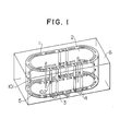
- Fig. l indicates this aspect.
- the arrow directed upward in a stripe magnetic domain 2 shows the direction of magnetization
- arrows l0l on the center line of the wall l show the direction of magnetization located at the wall center
- arrows l02 perpendicular to the wall l at the center line show the direction of magnetization at the center of the vertical Bloch line (hereinbelow called merely Bloch line).
- portions, where a pair of Bloch lines exist, correspond to "l" in data and portions, where no Bloch lines exist, correspond to "0".
- the Bloch line used as information carrier is a microstructure of the domain wall existing in the wall l surrounding the magnetic domain.
- the Bloch line can exist stably in the domain wall and propagate freely along the domain wall. Consequently, when a number of stripe magnetic domains are arranged at their predetermined positions and Bloch lines are made to exist in the domain wall, they behave just as bubbles propagating in a minor loop of a magnetic bubble memory. For this reason a Bloch line memory is a shift resistor type memory similarly to a magnetic bubble memory.
- Bloch line The existence of the Bloch line is known since long ago and it is verified by experiments and their analysis that the mobility of the magnetic domain is reduced by the existence of the Bloch line. Consequently, for the magnetic bubble memory, for which the magnetic domain should be shifted, the bubble domain containing Bloch lines is called hard bubble and it has been tried to prevent its generation. To the contrary, for the Bloch line memory device, the existence of this Bloch line is positively utilized.
- the physical size of the Bloch line is about l/l0 of the width of the stripe magnetic domain, where the Bloch line exists, and a number of Bloch lines can exist in one stripe magnetic domain.
- a number of Bloch lines can exist in one stripe magnetic domain.
- a garnet film having stripe magnetic domains l ⁇ m wide developed for a magnetic bubble memory it is possible to make about 5 ⁇ l06 Bloch lines exist per l cm3. Therefore, in the case where 2 Bloch lines are paired in the information medium, it is possible to realize a memory of 256 M bit/cm2.
- Bloch line memory device can have a large memory capacity, apart from the fact that the size is extremely small. It is due to the fact that in the Bloch line memory the magnetic field in the vertical direction is used for the propagation of information, while in the magnetic bubble memory information carriers are propagated by rotating an in-plane field. For this reason there is a high possibility that the propagation pattern is simplified in a plane, what acts so as to make it easier to increase the density for this type of memory elements.
- Bloch lines are produced in this way. Further two Bloch lines are always paired. Consequently the Bloch line memory is constituted by making one pair of Bloch lines correspond to one information.
- the read-out of information is effected, after having transformed the presence or absence of the Bloch line into the presence or absence of the bubble domain.
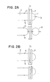
- the transformation of the Bloch line into the bubble domain is effected by the method described by Konishi in an article published in IEEE Trans. Mag. l9 , No. 5 (l983) p. l838 - p. l840 and p. l84l - p. l843. That is, when a pair of Bloch lines exist, the direction of magnetization in the domain wall is reversed at the pair of Bloch lines as a border, as indicated in Fig. l. When a pair of Bloch lines arrive at the stripe magnetic domain head, variations in this magnetization structure give rise to variations in chopping properties.
- Fig. 2 is a top view of the element indicated in Fig. l, in which also the direction of magnetization seen from above is indicated by arrows.
- the presence or absence of the Bloch lines can be transformed into the presence or absence of the bubble.
- Bloch line memory It is possible to realize a Bloch line memory by forming a write-in, a memory and a read-out function portion described above in one element.
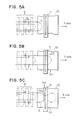
- Fig. 3A indicates a case where a pair of Bloch lines 4 arrive at the head portion of a stripe magnetic domain 2 and on the other hand Fig. 3B indicates a case where there are no pair of Bloch lines. In the two states, comparing the directions of the magnetizations 5 of the domain wall l, it can be seen that the two are same.
- the magnetization of the domain wall varies, depending on whether a pair of Bloch lines exist or not, but the magnetization doesn't vary, depending on whether a pair of Bloch lines exist or not. This reason is that the magnetization reversed by one Bloch line is reversed again by the other Bloch line so that the direction of the magnetization returns finally to the initial one. For this reason, since the direction of the magnetizations 5 doesn't vary depending on the presence or absence of the pair of Bloch lines only by the prior art method, it can be understood that its presence or absence cannot be transformed into the presence or absence of the magnetic bubble domain.
- JP-A-59-l0l092 As measures for resolving this problem a method is disclosed in JP-A-59-l0l092.
- electric current is made to flow through a conductor superposed on the chopping conductor so that the position of the pair of Bloch lines is held and reading-out is carried out by effecting the chopping operation between the pair of Bloch lines.
- the presence or absence of the pair of Bloch lines can be transformed into the presence or absence of the bubble domain and thus the reading-out according to the prior art techniques is realized.
- the object of this invention is to provide a practical Bloch line memory device, in which a pair of Bloch lines represent one bit information and a method for operating same.
- a Bloch line memory device is constructed as follows, in order to transform a pair of Bloch lines located at the head portion of the stripe magnetic domain into a magnetic bubble domain.
- the pair of Bloch lines have domain walls surrounded by the pair therebetween.
- means for applying an in-plane magnetic field having a component, which is approximately parallel to the direction of magnetization that the domain walls have, is disposed at the proximity of the head portion of the stripe magnetic domain.
- the direction of this in-plane magnetic field is so determined that it is parallel and opposite e.g. to the direction, along which the stripe magnetic domain stretches (Y axis direction).
- one of the Bloch lines becomes more distant from the head portion of the stripe magnetic domain and the other is held stably at the head portion of the stripe magnetic domain.
- a stripe magnetic domain chopping means disposed at the proximity of the head portion of the stripe domain chops the stripe magnetic domain, leaving the state in which the in-plane magnetic field is applied, so that it is transformed into the magnetic bubble domain, which is then detected by a magnetic bubble domain detecting means. After that, the application of the in-plane magnetic field is stopped.
- the stripe magnetic domain chopping means a hair-pin shaped conductor disposed in the direction perpendicular to that of the stretching of the stripe magnetic domain or two conductors parallel to each other are used.
- the magnetic bubble domain detecting means e.g. a magnetic bubble domain detector utilizing the magneto-resistive effect by means of soft magnetic materials is known.
- the presence or absence of the pair of Bloch lines at the head portion of the stripe magnetic domain corresponds to whether the stripe magnetic domain is chopped or not and in turn whether it is transformed into the magnetic bubble domain or not. Consequently, according to this invention, it is possible to realize a practical Bloch line memory device.
- the basic structure of the Bloch line memory consists of a stripe magnetic domain stabilizing pattern ll and a stripe magnetic domain 2.
- a pattern formed by scooping a magnetic film about l ⁇ m thick is used as means for stabilizing stripe magnetic domains.
- Pairs of Bloch lines can move freely in the domain wall.
- Two methods are conceived for shifting these pairs of Bloch lines.
- One of them is a method, by which a magnetic field perpendicular to the surface of the film is applied thereto, and a gyroscopic force acting on the magnetization is utilized.
- the other is a method, by which an in-plane magnetic field parallel to the plane, where the magnetic film exists, is utilized.
- the pairs of Bloch lines are freely shifted by either one of the methods.
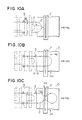
- a pattern 9 indicated in Fig. 4 is used as this means.
- Fig. 4A shows the state before the reading-out.
- a pair of Bloch lines 4 is located at the head portion of a stripe magnetic domain 2.
- One 4-l of the splitted Bloch lines is moved to the exterior of a conductor l0 by the magnetic field generated by the conductor l0.
- the other Bloch line 4-2 is located stably at the head portion of the stripe magnetic domain.
- This separation takes different periods of time, depending on the propagated distance of the Bloch lines. Usually, supposing that the conductor 5 is about 40 ⁇ m wide, it takes about 500 nano sec.
- the chopped magnetic domain 8 is detected by a method identical to that of the usual bubble memory techniques and thus the presence of the pair of Bloch lines can be read-out as digital data.
- the magnetization 5 Since there are no Bloch lines at the proximity of the head portion of the stripe magnetic domain, the magnetization 5 has different directions at the upper and the lower sides of the domain wall of the stripe magnetic domain, as indicated in Fig. 5B. In such a state it is difficult to chop the magnetic domain and no magnetic domain is chopped, if a chopping current I c2 is chosen.
- a conductor l0, 40 ⁇ m wide was used as means generating the in-plane magnetic field for splitting the pair of Bloch lines.
- the width of this conductor is so chosen that the in-plane magnetic field is generated with a high efficiency and usually it is thought that it is suitably from several to about l00 times as wide as the stripe magnetic domain. When it is still wider, the effective area of the device is reduced and thus it is not efficacious. To the contrary, when it is narrower than that, it is not desirable for generating the in-plane magnetic field with a high efficiency.
- a high coercive force film magnetized in the in-plane direction generates a stray in-plane magnetic field in the in-plane direction.
- the pair of Bloch lines are splitted and thus it becomes possible to read-out them.
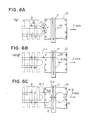
- Figs. 6A, 6B and 6C indicate this structure.
- a pattern made of Tb-Fe-Co, etc. having its axis of easy magnetization in the in-plane direction (hereinbelow called in-plane magnetization film pattern) is disposed at the proximity of the head portion of the stripe magnetic domain.
- the in-plane magnetic field leaking out from the in-plane magnetization film has the direction H c ′.
- the head portion of the stripe magnetic domain is stretched by applying a magnetic field - ⁇ H B , which is opposite to the vertical bias magnetic field H B , as indicated in Fig. 6B.
- the pair of Bloch lines are splitted, sensing the in-plane magnetic field, and thus it becomes possible to read-out them, just as in the case where the conductor is used, as described above.
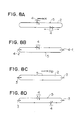
- Fig. 8A indicates the stripe magnetic domain 2.
- Two pairs of Bloch lines 4 exist on the periphery of one stripe magnetic domain 2.
- the directions of the magnetizations between the pairs of Bloch lines are opposite to each other.
- Fig. l this is because the magnetizations rotate continuously along the domain wall.
- a magnetic field H having the same direction as that of the magnetization in the region comprised between the pair of Bloch lines existing at the lower side of the domain wall is applied, the lower pair of Bloch lines are splitted and move to the two head portions of the stripe magnetic domain. For this reason, the information, which this pair of Bloch lines has disappears (Fig. 8B).
- Fig. 8C indicates this aspect.
- the Block lines 3 can exist stably at both the head portions.
- the pair of Bloch lines are written-in, owing to the continuity of the magnetization direction described above, the magnetization between the pair of Bloch lines is always opposite to that of the magnetic field Hip (Fig. 8D). For this reason, whether the pair of Bloch lines exist at the side, upper or lower, of the domain wall, they are not splitted and can exist stably.
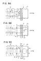
- FIG. 9A indicates the case where the Bloch line 3 described above and a pair of Bloch lines 4 corresponding to an information "l" exist at the head portion of the stripe magnetic domain.
- Fig. l0A indicates the state, where only the Bloch line 3 exists at the head portion of the stripe magnetic domain.
- the Bloch line 3 is shifted to the position indicated in Fig. l0B.
- the Bloch line is shifted along the side, upper or lower, of the domain wall, the magnetizations of the domain wall after the shift are opposite to each other at the upper and lower sides of the domain wall. Therefore, even by the chopping operation indicated in Fig. l0C, no magnetic domain is chopped. Consequently reading-out the information is realized by detecting the presence or absence of the chopped magnetic domain by using means identical to that according to the prior art techniques, just as in Embodiment l.
Landscapes
- Hall/Mr Elements (AREA)
- Magnetic Heads (AREA)
Applications Claiming Priority (2)
| Application Number | Priority Date | Filing Date | Title |
|---|---|---|---|
| JP4177686 | 1986-02-28 | ||
| JP41776/86 | 1986-02-28 |
Publications (3)
| Publication Number | Publication Date |
|---|---|
| EP0240135A2 true EP0240135A2 (de) | 1987-10-07 |
| EP0240135A3 EP0240135A3 (en) | 1989-11-02 |
| EP0240135B1 EP0240135B1 (de) | 1993-05-12 |
Family
ID=12617775
Family Applications (1)
| Application Number | Title | Priority Date | Filing Date |
|---|---|---|---|
| EP87301591A Expired - Lifetime EP0240135B1 (de) | 1986-02-28 | 1987-02-24 | Blochliniespeicheranordnung und Verfahren zu deren Betrieb |
Country Status (4)
| Country | Link |
|---|---|
| US (1) | US5050122A (de) |
| EP (1) | EP0240135B1 (de) |
| JP (1) | JPS62275383A (de) |
| DE (1) | DE3785787T2 (de) |
Families Citing this family (1)
| Publication number | Priority date | Publication date | Assignee | Title |
|---|---|---|---|---|
| US9048410B2 (en) | 2013-05-31 | 2015-06-02 | Micron Technology, Inc. | Memory devices comprising magnetic tracks individually comprising a plurality of magnetic domains having domain walls and methods of forming a memory device comprising magnetic tracks individually comprising a plurality of magnetic domains having domain walls |
Family Cites Families (4)
| Publication number | Priority date | Publication date | Assignee | Title |
|---|---|---|---|---|
| US4001794A (en) * | 1975-04-21 | 1977-01-04 | International Business Machines Corporation | Method and apparatus for controlled generation of wall topology in magnetic domains |
| US4583200A (en) * | 1982-10-18 | 1986-04-15 | Nec Corporation | Magnetic memory device capable of memorizing information in a stripe domain in the form of a vertical Bloch line pair |
| JPS59101092A (ja) * | 1982-12-02 | 1984-06-11 | Nec Corp | 磁気記憶方法 |
| JPS61248296A (ja) * | 1985-04-25 | 1986-11-05 | Nec Corp | 磁気記憶素子 |
-
1987
- 1987-02-19 US US07/016,656 patent/US5050122A/en not_active Expired - Fee Related
- 1987-02-20 JP JP62035520A patent/JPS62275383A/ja active Pending
- 1987-02-24 DE DE8787301591T patent/DE3785787T2/de not_active Expired - Fee Related
- 1987-02-24 EP EP87301591A patent/EP0240135B1/de not_active Expired - Lifetime
Also Published As
| Publication number | Publication date |
|---|---|
| EP0240135A3 (en) | 1989-11-02 |
| EP0240135B1 (de) | 1993-05-12 |
| DE3785787T2 (de) | 1993-08-12 |
| DE3785787D1 (de) | 1993-06-17 |
| JPS62275383A (ja) | 1987-11-30 |
| US5050122A (en) | 1991-09-17 |
Similar Documents
| Publication | Publication Date | Title |
|---|---|---|
| EP0106358B1 (de) | Magnetische Speicheranordnung fähig zum Speichern von Informationen in einer Banddomäne in der Gestalt eines senkrechten Blochlinienpaares | |
| EP0255044B1 (de) | Blochlinien-Speichereinrichtung | |
| US4162537A (en) | Magnetic bubble memory | |
| EP0240135A2 (de) | Blochliniespeicheranordnung und Verfahren zu deren Betrieb | |
| CA1109150A (en) | Gap tolerant bubble domain propagation circuits | |
| US3982234A (en) | Hard-magnetic film overlay apparatus and method for magnetic mobile domain control | |
| US4528645A (en) | Magnetic bubble memory device | |
| US3876994A (en) | Planar bias field control of magnetic bubble domain apparatus | |
| CA1058750A (en) | Field-accessed magnetic bubble mutually exclusive circuits with common elements | |
| US4142247A (en) | Conductor-driven magnetic bubble memory with an expander-detector arrangement | |
| US3736577A (en) | Domain transfer between adjacent magnetic chips | |
| US3713119A (en) | Domain propagation arrangement | |
| US3774182A (en) | Conductor-pattern apparatus for controllably inverting the sequence of a serial pattern of single-wall magnetic domains | |
| CA1187175A (en) | Magnetic bubble memory device and method for operating the same | |
| US4881198A (en) | Duplicator in a magnetic bubble memory and process for duplicating bubbles therein | |
| US4949304A (en) | Bloch line memory device | |
| CA1197924A (en) | Magnetic bubble memory device | |
| US4027297A (en) | Gapless magnetic bubble propagation path structure | |
| US4228523A (en) | Conductor access bubble memory arrangement | |
| CA1086861A (en) | Integrated bubble nucleator | |
| EP0263530B1 (de) | Blochzeilenspeicheranordnung | |
| US4167790A (en) | Magnetic bubble domain gate arrangement | |
| Wu et al. | Computer simulation of magnetic bubble logic devices | |
| US5047978A (en) | Bloch line memory device | |
| US3947830A (en) | Complementary transition structures for magnetic domain propagation |
Legal Events
| Date | Code | Title | Description |
|---|---|---|---|
| PUAI | Public reference made under article 153(3) epc to a published international application that has entered the european phase |
Free format text: ORIGINAL CODE: 0009012 |
|
| AK | Designated contracting states |
Kind code of ref document: A2 Designated state(s): DE FR GB |
|
| PUAL | Search report despatched |
Free format text: ORIGINAL CODE: 0009013 |
|
| AK | Designated contracting states |
Kind code of ref document: A3 Designated state(s): DE FR GB |
|
| 17P | Request for examination filed |
Effective date: 19900321 |
|
| 17Q | First examination report despatched |
Effective date: 19910320 |
|
| GRAA | (expected) grant |
Free format text: ORIGINAL CODE: 0009210 |
|
| AK | Designated contracting states |
Kind code of ref document: B1 Designated state(s): DE FR GB |
|
| REF | Corresponds to: |
Ref document number: 3785787 Country of ref document: DE Date of ref document: 19930617 |
|
| ET | Fr: translation filed | ||
| PGFP | Annual fee paid to national office [announced via postgrant information from national office to epo] |
Ref country code: FR Payment date: 19931216 Year of fee payment: 8 |
|
| PGFP | Annual fee paid to national office [announced via postgrant information from national office to epo] |
Ref country code: GB Payment date: 19940214 Year of fee payment: 8 |
|
| PG25 | Lapsed in a contracting state [announced via postgrant information from national office to epo] |
Ref country code: DE Effective date: 19941101 |
|
| PG25 | Lapsed in a contracting state [announced via postgrant information from national office to epo] |
Ref country code: GB Effective date: 19950224 |
|
| GBPC | Gb: european patent ceased through non-payment of renewal fee |
Effective date: 19950224 |
|
| PG25 | Lapsed in a contracting state [announced via postgrant information from national office to epo] |
Ref country code: FR Effective date: 19951031 |
|
| REG | Reference to a national code |
Ref country code: FR Ref legal event code: ST |
|
| PLBE | No opposition filed within time limit |
Free format text: ORIGINAL CODE: 0009261 |