EP0236019A2 - Apparatus for reproducing a component color signal - Google Patents
Apparatus for reproducing a component color signal Download PDFInfo
- Publication number
- EP0236019A2 EP0236019A2 EP87301459A EP87301459A EP0236019A2 EP 0236019 A2 EP0236019 A2 EP 0236019A2 EP 87301459 A EP87301459 A EP 87301459A EP 87301459 A EP87301459 A EP 87301459A EP 0236019 A2 EP0236019 A2 EP 0236019A2
- Authority
- EP
- European Patent Office
- Prior art keywords
- signal
- color component
- write
- signals
- pair
- Prior art date
- Legal status (The legal status is an assumption and is not a legal conclusion. Google has not performed a legal analysis and makes no representation as to the accuracy of the status listed.)
- Granted
Links
Images


Classifications
-
- H—ELECTRICITY
- H04—ELECTRIC COMMUNICATION TECHNIQUE
- H04N—PICTORIAL COMMUNICATION, e.g. TELEVISION
- H04N9/00—Details of colour television systems
- H04N9/79—Processing of colour television signals in connection with recording
- H04N9/87—Regeneration of colour television signals
- H04N9/89—Time-base error compensation
- H04N9/893—Time-base error compensation using an analogue memory, e.g. a CCD shift register, the delay of which is controlled by a voltage controlled oscillator
-
- Y—GENERAL TAGGING OF NEW TECHNOLOGICAL DEVELOPMENTS; GENERAL TAGGING OF CROSS-SECTIONAL TECHNOLOGIES SPANNING OVER SEVERAL SECTIONS OF THE IPC; TECHNICAL SUBJECTS COVERED BY FORMER USPC CROSS-REFERENCE ART COLLECTIONS [XRACs] AND DIGESTS
- Y10—TECHNICAL SUBJECTS COVERED BY FORMER USPC
- Y10S—TECHNICAL SUBJECTS COVERED BY FORMER USPC CROSS-REFERENCE ART COLLECTIONS [XRACs] AND DIGESTS
- Y10S414/00—Material or article handling
- Y10S414/135—Associated with semiconductor wafer handling
- Y10S414/141—Associated with semiconductor wafer handling includes means for gripping wafer
Definitions
- the present invention relates to an apparatus which reproduces a pair of color component signals whose time axes have been compressed and which have sequentially been recorded in a time division mode on each track of a recording medium other than that on which, for example, a luminance signal is recorded.
- a color video signal is separated into a luminance signal and a pair of color component signals (R-Y) and (B-Y). These separated signals are conventionally recorded on different tracks.
- the time axes of the pair of color component signals (R-Y) and (B-Y) are compressed 1/2 so as to be compressively recorded on the corresponding tracks within a time interval of one horizontal period.
- the color component signals thus recorded are written into a memory in response to a write clock signal having a predetermined frequency and are read out of the memory in response to a read clock signal having a frequency half the write clock signal frequency.
- the time axes of the pair of color component signals (R-Y) and (B-Y) are expanded to provide the interval of the original color component signals.
- misoperation in which the write operation and read operation are partially overlapped often occurs so that normal reproduction operations cannot be carried out.
- VTR Video Tape Recorder
- a prephaser variable delay circuit
- skew transient time axis variation occurring immediately after the rotary magnetic head is switched
- the above-described object can be achieved by providing an apparatus for reproducing recorded tracks on a recording medium in which a pair of time-axis compressed color component signals have been sequentially recorded in a time division mode, the reproduced color component signals being time-axis expanded characterised in that the apparatus comprises:
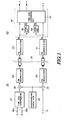
- a synchronizing signal derived from a synchronizing signal generation circuit 33 is added to a luminance signal Y transmitted to an input terminal 31 of a recording system generally denoted by numeral 30 by means of an adder 32. Then, the luminance signal derived from the adder 32 is FM modulated in an FM modulator 34 and is recorded on a magnetic tape 35 through a record head.
- a pair of color component signals R-Y and B-Y respectively transmitted to the input terminals 36a and 36b are time-axis compressed by 1/2.
- the chrominance component signals R-Y and B-Y are sequentially transmitted from the compression circuit 37: Thereafter, a synchronizing signal which is derived from the synchronizing signal generation circuit 33 is added to the compressed chrominance component signals in an adder 38.
- the chrominance component signals derived from the adder 38 is FM modulated in an FM modulator 39.
- the synchronizing signal is used as a reference pulse in order to adjust the time difference between the luminance and chrominance signals recorded in different channels and facilitate the synchronizing signal separation thereof.
- the synchronizing signal i.e., the reference pulse, is added in a rear portion of a horizontal synchronizing pulse of the luminance signal.
- the respective lHs (one horizontal scanning interval) of the chrominance signals are time-axis compressed to 1/2Hs and arranged sequentially in a time division mode. Then, the synchronizing signal (reference pulse) is also added to the compressed chrominance component signals in corresponding portions to which the synchronizing signal is added to the luminance signal.
- a signal reproduced from the recording track of the magnetic tape 35 on which the luminance signal is recorded is FM demodulated in an FM demodulator 41.
- a synchronizing signal YS (or the reference pulse) of the luminance signal S y is transmitted to a time axis expansion circuit 43.
- a time division time-axis compressed chrominance signal S reproduced from the chrominance signal recording track of the magnetic tape 35 via the playback head and FM demodulated by means of an FM demodulator 45 is supplied to a time axis expansion circuit 43 installed in the time axis processing circuit 42.
- a synchronizing signal CS is separated from a synchronizing signal separation circuit 46 and is supplied to the time axis expansion circuit 43.
- the synchronizing signal CS of the time division time-axis compressed signal S is actually the reference pulse described above.
- a pair of the component color signals which are respectively time-axis compressed to 1/2H are arranged between the respectively adjacent synchronizing signals CS corresponding to 1H (one horizontal interval).
- the luminance signal and time-axis expanded pair of color component signals are outputted from the time axis processing circuit 42 with their time-axis variations eliminated.
- an input terminal 51 receives the luminance signal S which is FM demodulated, e.g., by means of an FM demodulator 41.
- An input terminal 52 receives a time division time-axis compressed chrominance signal S c which has been FM (Frequency Modulation) demodulated by means of an FM demodulator 45 shown in Fig. 1.
- a chrominance signal S c is delayed by 1H (one horizontal scanning interval) with respect to the luminance signal S y when the chrominance signal S c is time-compressed in the time axis compression circuit 43.
- the luminance signal Sy derived from an input terminal 51 is advanced by 1H with respect to the chrominance signal S c .
- the luminance signal S y is delayed by 3H by means of a delay circuit 53.
- a synchronizing signal YS is separated in the synchronizing signal separation circuit 54.
- a signal S c from an input terminal 52 is transmitted to a variable delay circuit 55 using a CCD having a delay amount of about 1H.
- the two synchronizing signals YS and CS from each synchronizing signal separation circuit 54, 56 are transmitted to a phase comparison circuit 57 for detecting the phase difference between the synchronizing signals YS and CS.
- An output of the phase comparison circuit 57 is supplied to an voltage controlled oscillator (VCO) 58, the oscillating frequency of which is controlled according to the phase difference between signals YS and CS.
- VCO voltage controlled oscillator
- An output pulse from the VCO 58 is used as a drive clock of the CCD constituting the variable delay circuit 55.
- a signal S c from the variable delay circuit 55 is synchronized with the luminance signal S y .
- the circuitry comprising the phase comparison circuit 57, VCO 58 and the variable delay circuit (CCD) 55 is called a prephaser circuit and corrects the time difference between the luminance signal and chrominance signal.
- the synchronizing signal YS from the synchronizing signal separation circuit 54 is supplied to a VCO 61.
- the VCO 61 produces a pulse signal whose phase has been adjusted to the signal YS and whose frequency is, for example, 720 f H (f H denotes the horizontal frequency).
- the pulse signal having the frequency of 720 f H is frequency divided into a clock signal having a frequency of 360 f H by means of a 1/2 divider 62 and the divided clock signal is fed to a clock generator 63 as a read clock RCK.
- the synchronizing signal CS from the synchronizing signal separation circuit 56 is fed to a VCO 64 which produces a pulse signal whose phase is synchronized with the signal CS and having a frequency of 720 f H ,
- the pulse signal outputted from the VCO 64 is sent to the clock generator 63 as a write clock WCK.
- CCDs 71, 72, 73, and 74 constituting shift registers which receive the signal from the variable delay circuit 55.
- the write and read operations for these CCDs 71, 72, 73, and 74 are controlled respectively by means of clocks CK1, CK2, CK3, and CK4 from the clock generator 63 so as to time expand the time axis of an input signal from each CCD.
- the output signal from the CCD 71 is transmitted to terminal a of changeover switch 75
- the output signal from the CCD 72 is transmitted to terminal b of changeover switch 76
- the output signal of the CCD 73 is transmitted to terminal b of the changeover switch 75
- the output signal of the CCD 74 is transmitted to terminal b of the changeover switch 76, respectively.
- the one of the color component signals R-Y is obtained from an output terminal 77, while the other color component signal B-Y is obtained from another output terminal 78.
- a time division time-axis compressed chrominance signal S from the variable delay circuit 55 is advanced by 1H with respect to the luminance signal S y from the 3H delay circuit 53. This is because the luminance signal is delayed by 3H in 3H delay circuit 53 while the chrominance signal is delayed totally by 2H in the compression circuit 37 during recording and the variable delay circuit (CCD) 55.
- CCD variable delay circuit
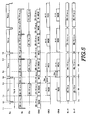
- the time division time-axis compressed chrominance signals (R-Y) n+1 , (B-Y) n+1 in the order of (n+l)H are sequentially arranged during 1/2 horizontal intervals(times t 1 and t 2 and times t 2 and t 3 ) with respect to the luminance signal Y n in the order of nH arranged at an 1H interval of times t 1 and t 3 .
- a write clock WCK having a frequency of 720 f H is supplied for an interval of a front half 1/2H (times t 1 to t 2 ) of the 1H interval of times t 1 and t 3 Accordingly, a signal component (R-Y) n+1 of the time division time-axis compressed chrominance signal S c is written into the CCD 71 between the times t, and t 2 (front half 1/2H interval).
- a write clock WCK having a frequency of 720 f H is supplied for an interval of the back half 1/2H (times t 2 to t 3 ) thereof.
- a signal (B-Y) n+1 which is transmitted in the back half of the horizontal interval is written into the CCD 72 .
- Each color component signal (R-Y) n+1 , (B-Y) n+1 written into these CCDs 71, 72 is read out in response to clocks CKl, CK2 during the next 1H interval between the times t 3 and t 5 .
- the frequency of a read clock RCK is selected as 360 f H , 1/2 of the write clock WCK, so that the chrominance signals read out from the CCDs are expanded twice and thereby the chrominance signal having the original time axis will be generated therefrom.
- a delay of 1H occurs in the processing circuit 42 so that the delayed chrominance signal is aligned in time with the luminance signal. That is, the chrominance signals (R-Y) n+1 , (B-Y) n+1 produced from the changeover switches 75, 76 between times t 3 and t 5 are the same (n+l)H order signals as the luminance signal Y n+1 .
- D w shown in Fig. 3 denotes a permissible interval (so called, a window) between a write operation and read operation in each of the CCDs 71 through 74.
- the pair of CCDs 71 and 72 described above thus, carries out the time axis expansions of the pair of color component signals R-Y, B-Y, respectively. Since a 2H interval is required to perform the time axis expansion of the 1H signal, the other pair of CCDs 73 and 74 are provided so that the read and write operations of the 2H interval are carried out alternately between the two pair of CCDs.
- the changeover switches 75, 76 are switched at every horizontal interval to select the output signals from the respective CCD pairs, alternately.
- the pair of color component signals R-Y, B-Y are produced from the respective output terminals 77, 78.
- the permissible interval between the write and read operations in the respective CCDs 71 through 74, the window D can last only approximately + 1 to 2.5 microseconds. Therefore, if a time axis error (jitter) between the luminance signal and chrominance signal exceeds the permissible interval, the misoperation in which the write operation and read operation are partially ovelapped often occurs so that normal reproducing operations cannot be carried out.
- a time axis error jitter
- the object of the present invention is to provide an apparatus for reproducing a component color signal having a signal processing circuit which can solve the above-described problem.
- an input terminal 1 receives the luminance signal S y which has been FM demodulated and derived from the FM demodulation circuit 41 shown in Fig. 1.
- Another input terminal 2 receives the chrominance signal (time-divided time-axis compressed chrominance signal) S c from the FM demodulator 45.
- the luminance signal S received at the input terminal 1 shown in Fig. 4 is delayed up to 1.25H (1 1/4H), as shown in Fig. 5, with respect to the chrominance signal S c received at another input terminal 2.
- the FM demodulated luminance signal Sy needs to be delayed by 2 1/4H by means of a delay circuit such as a CCD.
- the luminance signal S y is always delayed by 1 1/4H with respect to the chrominance signal S c at the respective input terminals 1 and 2.
- the luminance signal Y n+1 in the order of (n+1)H is arranged in one horizontal interval from time t 5 to time t 8 which has been delayed by 1 1/4H.
- the luminance signal S y derived from the input terminal 1 is supplied to a synchronizing signal separation circuit 3 to separate a synchronizing signal (the above-described reference pulse) YS.
- This synchronizing signal YS is then fed to a VCO (Voltage Controlled Oscillator) 4.
- the VCO 4 produces a pulse signal whose phase is locked to that of the above-described signal YS and whose frequency is, for example, 720 f H (f H denotes a horizontal frequency).
- the pulse signal having 720 f H is divided into a pulse signal having 360 f H by means of a 1/2 divider 5.
- the frequency divided pulse signal is supplied to RCK terminal of a clock generation circuit 6 as a read clock RCK.
- the chrominance signal S c derived from the input terminal 2 is supplied to a synchronizing signal separation circuit 7 to separate a synchronizing signal (above-described reference signal) CS.
- the synchronizing signal CS is then fed to a VCO 8.
- the VCO 8 produces a pulse signal 720 f H (f H . denotes the horizontal frequency) and having a phase locked to the above-described signal CS and the pulse signal derived from the VCO 8 is supplied to a WCK terminal of the clock generation circuit 6 as a write clock WCK.
- the above-described synchronizing signals YC, CS are also supplied to the clock generation circuit 6 for determining read and write reference timings of CCDs, as will be described later.
- the chrominance signal S c in a time division time-axis compressed state derived from the input terminal 2 is delayed by 1/2H by means of a CCD 10 constituting time delay means so that the pair of color component signals R-Y, B-Y are shifted so that their phases become in line with each other. That is to say, as shown in Fig. 5, a clock CKO transmitted from the clock generation circuit 6 to the CCD 10 is arranged such that a write clock WCK is supplied during a front half 1/2H interval (from times t 1 to t 3 ) of a 1H interval (from times t 1 to t 4 ) and a read clock R-WCK is supplied during a back half 1/2H interval (from times t 3 to t 4 ).
- the output pulse from the VCO 8 having a frequency of 720 f H is used for the write clock WCK and read clock R-WCK.
- the output signal S c ' from the CCD 10 is such that the color component signal R-Y arranged at the front half 1/2H interval of 1H interval of the chrominance signal S c is delayed by 1/2H and is in line with the color component B-Y signal arranged at the back half 1/2H interval of 1H interval of the chrominance signal S c .
- the pair of color component signals R-Y, B-Y mutually in line with each other are arranged respectively during each 1/2H interval corresponding to the middle positions for each lH interval of the luminance signal S .
- the number of shift stages in the CCD 10 which constitutes a shift register is set to 341 stages
- the number of pulses of each clock of WCK and R-WCK in the 1/2 H interval is 341.
- the signal write and read operations of the CCD 10 are carried out during an interval slightly shorter than a 1/2H interval.
- the write and read operations are alternately carried out at every half line periods for each 1H period.
- the clock CK2 for commonly controlling the pair of CCDs 11, 12 is such a signal having a period of 2H that the write clock WCK is generated during the 1/2H interval (from times t 3 to t 4 ) and the read clock RCK is generated during the 1H interval (from time t 5 to time t 8 ) of the luminance signal Sy which follows immediately after the end of the output of the WCK.
- An output signal having a frequency of 720 f H derived from the VCO 8 is used as the write clock WCK, which is synchronized with the synchronizing signal.CS of the chrominance signal S c .
- An output signal having a frequency of 360H from the divider 5 is used as the read clock RCK which is synchronized with the synchronizing signal YS of the luminance signal S y .
- the signal (R-Y) n+1 is read out with two times time-axis expansion during the 1H interval of times t 5 to t 8 of the synchronizing signal of the luminance signal.
- the chrominance signal (B-Y) n+1 is written in the CCD 12 during the 1/2H interval between times t 3 and t 4 .
- the output signal from the CCD 11 is transmitted to terminal a of a changeover switch 15, the output signal from the CCD 12 is sent to terminal a of a changeover switch 16, the output signal from the CCD 13 is transmitted to terminal b of the changeover switch 15, and the output signal from the CCD 14 is transmitted to terminal b of the changeover switch 16.
- These two changeover switches 15, 16 are alternately switched at every horizontal interval to select each terminal a, b of both switches-15, 16 in response to a switching control signal having a frequency of 1/2 f (2H period) and derived from the clock generator 6.
- the changeover switch 15 provides one of the color component signals, R-Y, from an output terminal 17 and the changeover switch 16 provides the other color component signal, B-Y, from an output terminal 18.
- the pair of the color component signals are synchronized with the luminance signal.
- a write clock interval is arranged at a center position of a non-read interval (lH) sandwiched between read clock output intervals (lH), approximately 1/4H interval can be secured as the permissible interval, the so called window D , before and after the write clock output interval.
- the window width of the window D w is wide enough to carry out the correction of the time axis error between the luminance signal and color component signal during the reproduction mode including the transient time axis variation (so called, skews) generated when the rotary magnetic heads are switched.
- the circuit scale is reduced, low power consumption is achieved, and, as different from the previously proposed signal processing circuit, limiter and Y-C phase adjustments required for the prephaser circuit is not necessary, required labor costs can accordingly be reduced.
- the time axis processing operation in the preferred embodiment is a start-and-stop method in which the read and write operations are separated with respect to time, the tracking capability for the transient and abrupt time axis variation becomes remarkably high as compared with the prephaser method in which the delay time is continuously varied. Consequently, ill effects such as noise and discrepancies between the luminance picture and the color picture will not occur
- the present invention is not limited only to the above-described preferred embodiment.
- the phase alignment between the pair of color component signals whose time axes are expanded and luminance signal may be made.
- the write clock operation during the time axis expansion operation may be arranged at a position deviated forward or rearward from the center position between the adjacent two read clock intervals. It should,however, be noted that the window length would then be asymmetrical in the positive and negative directions.
- the delay amount is accurately set to 1/2H (the number of CCD stages is 360) so that the write clock WCK (having the frequency of 720 f H) may directly be inputted to the CCD 10. Since in the apparatus for reproducing the component color signal according to the present invention the permissible interval (window) between the write and read operations for the shift register such as CCDs used for the time axis expansion can be relatively wide, circuit construction of a small scale not requiring the prephaser can be achieved. Furthermore, low power consumption and simple adjustment can be achieved and tracking capability for the transient time axis variation (skews), as compared with the prephaser circuit can remarkably be improved.
Abstract
Description
- The present invention relates to an apparatus which reproduces a pair of color component signals whose time axes have been compressed and which have sequentially been recorded in a time division mode on each track of a recording medium other than that on which, for example, a luminance signal is recorded.
- To achieve a record/reproduction of a video signal having a high picture quality and high resolution, a color video signal is separated into a luminance signal and a pair of color component signals (R-Y) and (B-Y). These separated signals are conventionally recorded on different tracks. At this recording time, the time axes of the pair of color component signals (R-Y) and (B-Y) are compressed 1/2 so as to be compressively recorded on the corresponding tracks within a time interval of one horizontal period. During the reproduction operation, the color component signals thus recorded are written into a memory in response to a write clock signal having a predetermined frequency and are read out of the memory in response to a read clock signal having a frequency half the write clock signal frequency. In this way, the time axes of the pair of color component signals (R-Y) and (B-Y) are expanded to provide the interval of the original color component signals. At this time, if a sufficient interval between the write operation and read operation is not provided, misoperation in which the write operation and read operation are partially overlapped often occurs so that normal reproduction operations cannot be carried out. Especially, in a VTR (Video Tape Recorder) in which rotary magnetic heads are switched at every half rotation , a prephaser (variable delay circuit) cannot follow a transient time axis variation occurring immediately after the rotary magnetic head is switched (so called skew). As a result, when the color component signals are inputted to a time axis expansion circuit, a normal time axis expansion for the color component signals cannot be achieved.
- With the above-identified problem in mind, it is an object of the present invention to provide an apparatus for reproducing a component color signal in a simple construction which enhances a tracking capability for a time variation of a reproduced signal (so called, skews) accompanied with a head switching, which prevents the misoperations due to an overlap of read and write operations by providing a wide interval (window) between the read and write operations in shift register and which achieves reduction of consumed power and simplification of adjustments.
- The above-described object can be achieved by providing an apparatus for reproducing recorded tracks on a recording medium in which a pair of time-axis compressed color component signals have been sequentially recorded in a time division mode, the reproduced color component signals being time-axis expanded characterised in that the apparatus comprises:
- (a) first means for shifiting one of said color component signals in the time-axis direction thereof;
- (b) a plurality of shift registers responsive to write and read clocks for time-expanding the pair of time axis compressed color component signals, one of the latter signals being derived from said first means; and
- (c) second means for controlling each of the write and read clocks so that intervals during which said write clock is generated are arranged at respective positions intermediate successive intervals during which the read clock is generated, whereby the original pair of color component signals before the time axis compression are reproduced.
- A more complete understanding of the present invention may be obtained from the following description taken in conjunction with the attached drawings in which:
- Fig. 1 is a circuit block diagram of a recording and reproducing system of a VTR to which a component color signal reproducing apparatus according to the present invention is applicable;
- Fig. 2 is a circuit block diagram of a previously proposed time axis processing circuit shown in Fig. 1;
- Fig. 3 is a timing chart for explaining an operation of the time axis processing circuit shown in Figs. 1 and 2;
- Fig. 4 is a circuit block diagram of a time axis processing circuit used in the reproducing apparatus of a preferred embodiment according to the present invention; and
- Fig. 5 is a timing chart for explaining an operation of the time axis processing circuit shown in Fig. 4.
- Reference will hereinafter be made to the drawings in order to facilitate understanding of the present invention.
- Fig. 1 shows a recording and reproducing system of a VTR to which the apparatus for reproducing the component color signal according to the present invention is applicable.
- Fig. 2 shows a previously proposed time axis processing circuit denoted by
numeral 42 shown in Fig. 1. - Fig. 3 shows a timing chart of representative signals for explaining an operation of the time axis expansion circuit shown in Figs. 1 and 2.
- Fig. 4 shows a detailed circuit block diagram of a time axis processing circuit used in the component color signal reproducing apparatus of a preferred embodiment according to the present invention.
- Fig. 5 shows a timing chart for explaining an operation of the time axis processing circuit shown in Fig. 4.
- In Fig. 1, a synchronizing signal derived from a synchronizing
signal generation circuit 33 is added to a luminance signal Y transmitted to aninput terminal 31 of a recording system generally denoted bynumeral 30 by means of anadder 32. Then, the luminance signal derived from theadder 32 is FM modulated in anFM modulator 34 and is recorded on amagnetic tape 35 through a record head. A pair of color component signals R-Y and B-Y respectively transmitted to theinput terminals signal generation circuit 33 is added to the compressed chrominance component signals in anadder 38. The chrominance component signals derived from theadder 38 is FM modulated in anFM modulator 39. It is herein noted that the synchronizing signal is used as a reference pulse in order to adjust the time difference between the luminance and chrominance signals recorded in different channels and facilitate the synchronizing signal separation thereof. The synchronizing signal, i.e., the reference pulse, is added in a rear portion of a horizontal synchronizing pulse of the luminance signal. The respective lHs (one horizontal scanning interval) of the chrominance signals are time-axis compressed to 1/2Hs and arranged sequentially in a time division mode. Then, the synchronizing signal (reference pulse) is also added to the compressed chrominance component signals in corresponding portions to which the synchronizing signal is added to the luminance signal. - In addition, in a reproducing system generally denoted by 40 shown in Fig. 1, a signal reproduced from the recording track of the
magnetic tape 35 on which the luminance signal is recorded is FM demodulated in anFM demodulator 41. Thereafter, a synchronizing signal YS (or the reference pulse) of the luminance signal Sy. demodulated by means'of theFM demodulator 41 derived from a synchronizingsignal separation circuit 44 is transmitted to a timeaxis expansion circuit 43. Next, a time division time-axis compressed chrominance signal S reproduced from the chrominance signal recording track of themagnetic tape 35 via the playback head and FM demodulated by means of anFM demodulator 45 is supplied to a timeaxis expansion circuit 43 installed in the timeaxis processing circuit 42. A synchronizing signal CS is separated from a synchronizingsignal separation circuit 46 and is supplied to the timeaxis expansion circuit 43. The synchronizing signal CS of the time division time-axis compressed signal S is actually the reference pulse described above. A pair of the component color signals which are respectively time-axis compressed to 1/2H are arranged between the respectively adjacent synchronizing signals CS corresponding to 1H (one horizontal interval). The luminance signal and time-axis expanded pair of color component signals are outputted from the timeaxis processing circuit 42 with their time-axis variations eliminated. - Next, in Fig. 2, an
input terminal 51 receives the luminance signal S which is FM demodulated, e.g., by means of anFM demodulator 41. Aninput terminal 52 receives a time division time-axis compressed chrominance signal Sc which has been FM (Frequency Modulation) demodulated by means of anFM demodulator 45 shown in Fig. 1. It is noted that a chrominance signal Sc is delayed by 1H (one horizontal scanning interval) with respect to the luminance signal Sy when the chrominance signal Sc is time-compressed in the timeaxis compression circuit 43. In other words, the luminance signal Sy derived from aninput terminal 51 is advanced by 1H with respect to the chrominance signal S c. The luminance signal Sy is delayed by 3H by means of adelay circuit 53. A synchronizing signal YS is separated in the synchronizingsignal separation circuit 54. A signal Sc from aninput terminal 52 is transmitted to avariable delay circuit 55 using a CCD having a delay amount of about 1H. The two synchronizing signals YS and CS from each synchronizingsignal separation circuit phase comparison circuit 57 for detecting the phase difference between the synchronizing signals YS and CS. An output of thephase comparison circuit 57 is supplied to an voltage controlled oscillator (VCO) 58, the oscillating frequency of which is controlled according to the phase difference between signals YS and CS. - An output pulse from the
VCO 58 is used as a drive clock of the CCD constituting thevariable delay circuit 55. A signal Sc from thevariable delay circuit 55 is synchronized with the luminance signal Sy. The circuitry comprising thephase comparison circuit 57,VCO 58 and the variable delay circuit (CCD) 55 is called a prephaser circuit and corrects the time difference between the luminance signal and chrominance signal. - In addition, the synchronizing signal YS from the synchronizing
signal separation circuit 54 is supplied to a VCO 61. The VCO 61 produces a pulse signal whose phase has been adjusted to the signal YS and whose frequency is, for example, 720 fH (fH denotes the horizontal frequency). The pulse signal having the frequency of 720 fH is frequency divided into a clock signal having a frequency of 360 fH by means of a 1/2divider 62 and the divided clock signal is fed to aclock generator 63 as a read clock RCK. On the other hand, the synchronizing signal CS from the synchronizingsignal separation circuit 56 is fed to aVCO 64 which produces a pulse signal whose phase is synchronized with the signal CS and having a frequency of 720 fH, The pulse signal outputted from theVCO 64 is sent to theclock generator 63 as a write clock WCK. In this embodiment, there are providedCCDs variable delay circuit 55. The write and read operations for theseCCDs clock generator 63 so as to time expand the time axis of an input signal from each CCD. In addition, the output signal from the CCD 71 is transmitted to terminal a ofchangeover switch 75, the output signal from theCCD 72 is transmitted to terminal b ofchangeover switch 76, the output signal of theCCD 73 is transmitted to terminal b of thechangeover switch 75, and the output signal of theCCD 74 is transmitted to terminal b of thechangeover switch 76, respectively. The one of the color component signals R-Y is obtained from an output terminal 77, while the other color component signal B-Y is obtained from anotheroutput terminal 78. The time axis expansion operation of the timeaxis processing circuit 42 will be described with reference to Fig. 3. A time division time-axis compressed chrominance signal S from thevariable delay circuit 55 is advanced by 1H with respect to the luminance signal Sy from the3H delay circuit 53. This is because the luminance signal is delayed by 3H in3H delay circuit 53 while the chrominance signal is delayed totally by 2H in thecompression circuit 37 during recording and the variable delay circuit (CCD) 55. Hence, as shown in Fig. 3, the time division time-axis compressed chrominance signals (R-Y)n+1, (B-Y)n+1 in the order of (n+l)H are sequentially arranged during 1/2 horizontal intervals(times t1 and t2 and times t2 and t 3) with respect to the luminance signal Yn in the order of nH arranged at an 1H interval of times t1 and t3. - For a clock CKl fed from the
clock generator 63 to the CCD 71, a write clock WCK having a frequency of 720 fH is supplied for an interval of afront half 1/2H (times t1 to t2) of the 1H interval of times t1 and t3 Accordingly, a signal component (R-Y)n+1 of the time division time-axis compressed chrominance signal Sc is written into the CCD 71 between the times t, and t2 (front half 1/2H interval). For a clock CK2 fed from theclock generator 63 to theCCD 72, a write clock WCK having a frequency of 720 fH is supplied for an interval of theback half 1/2H (times t2 to t3) thereof. As a result, a signal (B-Y)n+1 which is transmitted in the back half of the horizontal interval is written into the CCD 72. Each color component signal (R-Y)n+1, (B-Y)n+1 written into theseCCDs 71, 72 is read out in response to clocks CKl, CK2 during the next 1H interval between the times t3 and t5. The frequency of a read clock RCK is selected as 360 fH, 1/2 of the write clock WCK, so that the chrominance signals read out from the CCDs are expanded twice and thereby the chrominance signal having the original time axis will be generated therefrom. Thus, a delay of 1H occurs in theprocessing circuit 42 so that the delayed chrominance signal is aligned in time with the luminance signal. That is, the chrominance signals (R-Y)n+1, (B-Y)n+1 produced from the changeover switches 75, 76 between times t3 and t5 are the same (n+l)H order signals as the luminance signal Yn+1. It is noted that Dw shown in Fig. 3 denotes a permissible interval (so called, a window) between a write operation and read operation in each of the CCDs 71 through 74. - The pair of
CCDs 71 and 72 described above, thus, carries out the time axis expansions of the pair of color component signals R-Y, B-Y, respectively. Since a 2H interval is required to perform the time axis expansion of the 1H signal, the other pair ofCCDs respective output terminals 77, 78. - In such a time
axis expansion circuit 43 as shown in Figs. 1 and 2, the permissible interval between the write and read operations in the respective CCDs 71 through 74, the window D can last only approximately + 1 to 2.5 microseconds. Therefore, if a time axis error (jitter) between the luminance signal and chrominance signal exceeds the permissible interval, the misoperation in which the write operation and read operation are partially ovelapped often occurs so that normal reproducing operations cannot be carried out. - The object of the present invention is to provide an apparatus for reproducing a component color signal having a signal processing circuit which can solve the above-described problem.
- Construction and operation of the signal processing circuit according to the present invention will be described with reference to Figs. 1, 4, and 5.
- In Fig. 4, an
input terminal 1 receives the luminance signal Sy which has been FM demodulated and derived from theFM demodulation circuit 41 shown in Fig. 1. Anotherinput terminal 2 receives the chrominance signal (time-divided time-axis compressed chrominance signal) S c from theFM demodulator 45. It should be noted that the luminance signal S received at theinput terminal 1 shown in Fig. 4 is delayed up to 1.25H (1 1/4H), as shown in Fig. 5, with respect to the chrominance signal Sc received at anotherinput terminal 2. If, for example, the luminance signal Sy derived from theFM demodulator 41 is advanced by 1H with respect to the chrominance signal Sc, the FM demodulated luminance signal Sy needs to be delayed by 2 1/4H by means of a delay circuit such as a CCD. Thus, the luminance signal Sy is always delayed by 1 1/4H with respect to the chrominance signal Sc at therespective input terminals - Hence, for example, when the pair of color component signals (R-Y)n+1, (B-Y)n+1 in the order of (n+l)H are arranged in the time sharing mode whose time axes have been compressed to 1/2H within 1H interval (one horizontal interval) from time t1 to time t4 shown in Fig. 5, the luminance signal Yn+1 in the order of (n+1)H is arranged in one horizontal interval from time t5 to time t 8 which has been delayed by 1 1/4H.
- The luminance signal Sy derived from the
input terminal 1 is supplied to a synchronizingsignal separation circuit 3 to separate a synchronizing signal (the above-described reference pulse) YS. This synchronizing signal YS is then fed to a VCO (Voltage Controlled Oscillator) 4. TheVCO 4 produces a pulse signal whose phase is locked to that of the above-described signal YS and whose frequency is, for example, 720 fH (fH denotes a horizontal frequency). The pulse signal having 720 fH is divided into a pulse signal having 360 fH by means of a 1/2divider 5. The frequency divided pulse signal is supplied to RCK terminal of aclock generation circuit 6 as a read clock RCK. On the other hand, the chrominance signal Sc derived from theinput terminal 2 is supplied to a synchronizingsignal separation circuit 7 to separate a synchronizing signal (above-described reference signal) CS. The synchronizing signal CS is then fed to aVCO 8. TheVCO 8 produces a pulse signal 720 fH (fH . denotes the horizontal frequency) and having a phase locked to the above-described signal CS and the pulse signal derived from theVCO 8 is supplied to a WCK terminal of theclock generation circuit 6 as a write clock WCK. It is noted that the above-described synchronizing signals YC, CS are also supplied to theclock generation circuit 6 for determining read and write reference timings of CCDs, as will be described later. - The chrominance signal Sc in a time division time-axis compressed state derived from the
input terminal 2 is delayed by 1/2H by means of aCCD 10 constituting time delay means so that the pair of color component signals R-Y, B-Y are shifted so that their phases become in line with each other. That is to say, as shown in Fig. 5, a clock CKO transmitted from theclock generation circuit 6 to theCCD 10 is arranged such that a write clock WCK is supplied during afront half 1/2H interval (from times t1 to t3) of a 1H interval (from times t 1 to t4) and a read clock R-WCK is supplied during aback half 1/2H interval (from times t3 to t4). The output pulse from theVCO 8 having a frequency of 720 fH is used for the write clock WCK and read clock R-WCK. Hence, the output signal Sc' from theCCD 10 is such that the color component signal R-Y arranged at thefront half 1/2H interval of 1H interval of the chrominance signal Sc is delayed by 1/2H and is in line with the color component B-Y signal arranged at theback half 1/2H interval of 1H interval of the chrominance signal Sc. That is to say, for these chrominance signals Sc', Sc, the pair of color component signals R-Y, B-Y mutually in line with each other are arranged respectively during each 1/2H interval corresponding to the middle positions for each lH interval of the luminance signal S . Now, assuming that the number of shift stages in theCCD 10 which constitutes a shift register is set to 341 stages, the number of pulses of each clock of WCK and R-WCK in the 1/2H interval is 341. As a result, the signal write and read operations of theCCD 10 are carried out during an interval slightly shorter than a 1/2H interval. As apparent from Fig. 5, the write and read operations are alternately carried out at every half line periods for each 1H period. - Expansion:
- Next, the chrominance signal S ' delayed by means of the
CCD 10 is supplied to twoCCDs 11, 13 for time-axis expansion operations. On the other hand, the chrominance signals Sc from theinput terminal 2 are directly transmitted to twoCCDs CCD 10 has. A clock CK2 derived from theclock generator 6 is supplied to the pair ofCCDs 11, 12 to which the pair of color component signals R-Y and B-Y are respectively supplied. Another pair ofCCDs - The clock CK2 for commonly controlling the pair of
CCDs 11, 12 is such a signal having a period of 2H that the write clock WCK is generated during the 1/2H interval (from times t3 to t4) and the read clock RCK is generated during the 1H interval (from time t5 to time t 8) of the luminance signal Sy which follows immediately after the end of the output of the WCK. An output signal having a frequency of 720 fH derived from theVCO 8 is used as the write clock WCK, which is synchronized with the synchronizing signal.CS of the chrominance signal Sc. An output signal having a frequency of 360H from thedivider 5 is used as the read clock RCK which is synchronized with the synchronizing signal YS of the luminance signal Sy. Hence, in the CCD 11, after the color component signal (R-Y)n+1 has been written during the 1/2H interval between times t3 and t4, the signal (R-Y)n+1 is read out with two times time-axis expansion during the 1H interval of times t5 to t8 of the synchronizing signal of the luminance signal. At the same time, the chrominance signal (B-Y)n+1 is written in theCCD 12 during the 1/2H interval between times t3 and t4. During the 1H interval of times t5 and t8 the same signal (B-Y)n+1 is read out with the time axis expansion. In the same way as described above, these write and read operations are repreated respectively for each interval of 2H. It is noted that since a clock CK4 supplied in common to theCCDs CCDs CCDs 11, 12 but with a time delay (or time advance) of 1H. - Next, the output signal from the CCD 11 is transmitted to terminal a of a
changeover switch 15, the output signal from theCCD 12 is sent to terminal a of achangeover switch 16, the output signal from theCCD 13 is transmitted to terminal b of thechangeover switch 15, and the output signal from theCCD 14 is transmitted to terminal b of thechangeover switch 16. These two changeover switches 15, 16 are alternately switched at every horizontal interval to select each terminal a, b of both switches-15, 16 in response to a switching control signal having a frequency of 1/2 f (2H period) and derived from theclock generator 6. Hence, thechangeover switch 15 provides one of the color component signals, R-Y, from anoutput terminal 17 and thechangeover switch 16 provides the other color component signal, B-Y, from anoutput terminal 18. Thus, the pair of the color component signals are synchronized with the luminance signal. - The following is an explanation of the write and read operations for each 2H period on the basis of the above-described common clocks CK2, CK4.
- Since a write clock interval is arranged at a center position of a non-read interval (lH) sandwiched between read clock output intervals (lH), approximately 1/4H interval can be secured as the permissible interval, the so called window D , before and after the write clock output interval. The window width of the window Dw is wide enough to carry out the correction of the time axis error between the luminance signal and color component signal during the reproduction mode including the transient time axis variation (so called, skews) generated when the rotary magnetic heads are switched.
- Hence, since the above-described prephaser circuit is not necessary, the circuit scale is reduced, low power consumption is achieved, and, as different from the previously proposed signal processing circuit, limiter and Y-C phase adjustments required for the prephaser circuit is not necessary, required labor costs can accordingly be reduced. Furthermore, since the time axis processing operation in the preferred embodiment is a start-and-stop method in which the read and write operations are separated with respect to time, the tracking capability for the transient and abrupt time axis variation becomes remarkably high as compared with the prephaser method in which the delay time is continuously varied. Consequently, ill effects such as noise and discrepancies between the luminance picture and the color picture will not occur
- It is noted that the present invention is not limited only to the above-described preferred embodiment. For example, after the phase alignment of the pair of color component signals and time axis expansion using the common clocks, the phase alignment between the pair of color component signals whose time axes are expanded and luminance signal may be made. In addition, the write clock operation during the time axis expansion operation may be arranged at a position deviated forward or rearward from the center position between the adjacent two read clock intervals. It should,however, be noted that the window length would then be asymmetrical in the positive and negative directions. Furthermore, although in the above-described embodiment, a stop interval between the write and read intervals of the
CCD 10 which constitutes time delay means for the phase alignment of the color component signals is provided, the delay amount is accurately set to 1/2H (the number of CCD stages is 360) so that the write clock WCK (having the frequency of 720 f H) may directly be inputted to theCCD 10. Since in the apparatus for reproducing the component color signal according to the present invention the permissible interval (window) between the write and read operations for the shift register such as CCDs used for the time axis expansion can be relatively wide, circuit construction of a small scale not requiring the prephaser can be achieved. Furthermore, low power consumption and simple adjustment can be achieved and tracking capability for the transient time axis variation (skews), as compared with the prephaser circuit can remarkably be improved. - It will fully be understood by those skilled in the art that the foregoing description is made in terms of the preferred embodiment and various changes may be made without departing from the scope of the present invention which is defined by the appended claims.
Claims (12)
Priority Applications (1)
| Application Number | Priority Date | Filing Date | Title |
|---|---|---|---|
| AT87301459T ATE78654T1 (en) | 1986-02-28 | 1987-02-19 | DEVICE FOR REPRODUCTION OF A COLOR COMPONENT SIGNAL. |
Applications Claiming Priority (2)
| Application Number | Priority Date | Filing Date | Title |
|---|---|---|---|
| JP61043038A JPS62200890A (en) | 1986-02-28 | 1986-02-28 | Reproducing device |
| JP43038/86 | 1986-02-28 |
Publications (3)
| Publication Number | Publication Date |
|---|---|
| EP0236019A2 true EP0236019A2 (en) | 1987-09-09 |
| EP0236019A3 EP0236019A3 (en) | 1988-09-21 |
| EP0236019B1 EP0236019B1 (en) | 1992-07-22 |
Family
ID=12652739
Family Applications (1)
| Application Number | Title | Priority Date | Filing Date |
|---|---|---|---|
| EP87301459A Expired - Lifetime EP0236019B1 (en) | 1986-02-28 | 1987-02-19 | Apparatus for reproducing a component color signal |
Country Status (5)
| Country | Link |
|---|---|
| US (1) | US4774594A (en) |
| EP (1) | EP0236019B1 (en) |
| JP (1) | JPS62200890A (en) |
| AT (1) | ATE78654T1 (en) |
| DE (1) | DE3780483T2 (en) |
Cited By (1)
| Publication number | Priority date | Publication date | Assignee | Title |
|---|---|---|---|---|
| EP0228302A3 (en) * | 1985-12-27 | 1989-02-15 | Victor Company Of Japan, Limited | Color video signal recording and reproducing apparatus |
Families Citing this family (4)
| Publication number | Priority date | Publication date | Assignee | Title |
|---|---|---|---|---|
| GB2202709B (en) * | 1987-03-24 | 1991-05-01 | Sony Corp | Time base correcting apparatus |
| KR890015245A (en) * | 1988-03-30 | 1989-10-28 | 무라가미 류우이찌 | Magnetic recording and reproducing apparatus for obtaining a separate clock signal from the luminance and color components of the video signal |
| JPH0290880A (en) * | 1988-09-28 | 1990-03-30 | Fuji Photo Film Co Ltd | Reproducing device for fm modulated video signal |
| JP3094045B2 (en) * | 1991-12-16 | 2000-10-03 | 富士写真フイルム株式会社 | Digital electronic still camera and control method thereof |
Citations (1)
| Publication number | Priority date | Publication date | Assignee | Title |
|---|---|---|---|---|
| US4608609A (en) * | 1982-08-20 | 1986-08-26 | Sony Corporation | Apparatus for recording a color video signal |
Family Cites Families (8)
| Publication number | Priority date | Publication date | Assignee | Title |
|---|---|---|---|---|
| AU523619B2 (en) * | 1978-04-07 | 1982-08-05 | Sony Corporation | Video signal processing system |
| US4389678A (en) * | 1979-10-05 | 1983-06-21 | Nippon Electric Co., Ltd. | Digital time-base corrector for special motion reproduction by helical-scan VTR |
| US4399472A (en) * | 1980-06-11 | 1983-08-16 | Matsushita Electric Industrial Company, Limited | Phase difference compensation between separately recorded luminance and chrominance signals |
| JPS57160286A (en) * | 1981-03-28 | 1982-10-02 | Sony Corp | Time base correcting device |
| US4467368A (en) * | 1981-08-12 | 1984-08-21 | Robert Bosch Gmbh | Method and means for recording and playback of color television signals |
| JPS594279A (en) * | 1982-06-29 | 1984-01-11 | Sony Corp | Magnetic recorder and reproducer |
| JPS59172897A (en) * | 1983-03-22 | 1984-09-29 | Victor Co Of Japan Ltd | Clock pulse generating circuit in color video signal reproducing device |
| US4672469A (en) * | 1983-08-26 | 1987-06-09 | Victor Company Of Japan, Ltd. | Delay time adjusting system for video signal reproducing apparatus having heads scanning across multiple tracks |
-
1986
- 1986-02-28 JP JP61043038A patent/JPS62200890A/en active Pending
-
1987
- 1987-02-12 US US07/013,940 patent/US4774594A/en not_active Expired - Lifetime
- 1987-02-19 DE DE8787301459T patent/DE3780483T2/en not_active Expired - Fee Related
- 1987-02-19 EP EP87301459A patent/EP0236019B1/en not_active Expired - Lifetime
- 1987-02-19 AT AT87301459T patent/ATE78654T1/en not_active IP Right Cessation
Patent Citations (1)
| Publication number | Priority date | Publication date | Assignee | Title |
|---|---|---|---|---|
| US4608609A (en) * | 1982-08-20 | 1986-08-26 | Sony Corporation | Apparatus for recording a color video signal |
Cited By (1)
| Publication number | Priority date | Publication date | Assignee | Title |
|---|---|---|---|---|
| EP0228302A3 (en) * | 1985-12-27 | 1989-02-15 | Victor Company Of Japan, Limited | Color video signal recording and reproducing apparatus |
Also Published As
| Publication number | Publication date |
|---|---|
| DE3780483T2 (en) | 1993-02-25 |
| DE3780483D1 (en) | 1992-08-27 |
| EP0236019B1 (en) | 1992-07-22 |
| ATE78654T1 (en) | 1992-08-15 |
| JPS62200890A (en) | 1987-09-04 |
| US4774594A (en) | 1988-09-27 |
| EP0236019A3 (en) | 1988-09-21 |
Similar Documents
| Publication | Publication Date | Title |
|---|---|---|
| US5245430A (en) | Timebase corrector with drop-out compensation | |
| US4746996A (en) | Skew error correction circuit for video signal reproducing apparatus | |
| US4438456A (en) | Time base corrector | |
| US4916553A (en) | Video signal recording and reproducing method and apparatus | |
| EP0151538B1 (en) | Video tape recorder | |
| US4780769A (en) | Recording and reproducing apparatus for time compressed video signals wherein said signals are expanded and converted into two separate channels before recording | |
| US4090215A (en) | Electronic time base error correction methods and arrangements | |
| US4549224A (en) | Digital video tape recorder that can be used with different television systems | |
| EP0421486B1 (en) | Skew error correction circuit for video signal reproducing apparatus | |
| EP0236019B1 (en) | Apparatus for reproducing a component color signal | |
| KR950006247B1 (en) | Apparatus for reproducing component color video signals time-axia compressed on a recording medium using write clock signals centered between read clock signals | |
| JP2861160B2 (en) | Video signal playback device | |
| US4809097A (en) | Magnetic recording and reproducing apparatus | |
| US4760468A (en) | Color video signal recording and reproducing apparatus | |
| EP0231106B1 (en) | Magnetic recording and/or reproducing apparatus and methods | |
| US4972335A (en) | Video signal recording and reproducing apparatus and method suitable for recording video signals including horizontal scanning line signals | |
| EP0024850B1 (en) | Video signal recording and reproducing apparatus | |
| JP2529454B2 (en) | Recording and playback device | |
| JPH0666963B2 (en) | Color video signal playback device | |
| JPS60160276A (en) | Video signal processing unit | |
| JP2525883B2 (en) | Sync converter | |
| JP2832902B2 (en) | Video signal playback device | |
| JPS60217773A (en) | Skew distortion removing device | |
| JPH0546756B2 (en) | ||
| JPS6338156B2 (en) |
Legal Events
| Date | Code | Title | Description |
|---|---|---|---|
| PUAI | Public reference made under article 153(3) epc to a published international application that has entered the european phase |
Free format text: ORIGINAL CODE: 0009012 |
|
| 17P | Request for examination filed |
Effective date: 19870224 |
|
| AK | Designated contracting states |
Kind code of ref document: A2 Designated state(s): AT DE FR GB |
|
| PUAL | Search report despatched |
Free format text: ORIGINAL CODE: 0009013 |
|
| AK | Designated contracting states |
Kind code of ref document: A3 Designated state(s): AT DE FR GB |
|
| 17Q | First examination report despatched |
Effective date: 19910924 |
|
| GRAA | (expected) grant |
Free format text: ORIGINAL CODE: 0009210 |
|
| AK | Designated contracting states |
Kind code of ref document: B1 Designated state(s): AT DE FR GB |
|
| REF | Corresponds to: |
Ref document number: 78654 Country of ref document: AT Date of ref document: 19920815 Kind code of ref document: T |
|
| REF | Corresponds to: |
Ref document number: 3780483 Country of ref document: DE Date of ref document: 19920827 |
|
| ET | Fr: translation filed | ||
| PLBE | No opposition filed within time limit |
Free format text: ORIGINAL CODE: 0009261 |
|
| STAA | Information on the status of an ep patent application or granted ep patent |
Free format text: STATUS: NO OPPOSITION FILED WITHIN TIME LIMIT |
|
| 26N | No opposition filed | ||
| PGFP | Annual fee paid to national office [announced via postgrant information from national office to epo] |
Ref country code: DE Payment date: 20010212 Year of fee payment: 15 |
|
| PGFP | Annual fee paid to national office [announced via postgrant information from national office to epo] |
Ref country code: GB Payment date: 20010214 Year of fee payment: 15 |
|
| REG | Reference to a national code |
Ref country code: GB Ref legal event code: IF02 |
|
| PGFP | Annual fee paid to national office [announced via postgrant information from national office to epo] |
Ref country code: FR Payment date: 20020212 Year of fee payment: 16 |
|
| PGFP | Annual fee paid to national office [announced via postgrant information from national office to epo] |
Ref country code: AT Payment date: 20020213 Year of fee payment: 16 |
|
| PG25 | Lapsed in a contracting state [announced via postgrant information from national office to epo] |
Ref country code: GB Free format text: LAPSE BECAUSE OF NON-PAYMENT OF DUE FEES Effective date: 20020219 |
|
| PG25 | Lapsed in a contracting state [announced via postgrant information from national office to epo] |
Ref country code: DE Free format text: LAPSE BECAUSE OF NON-PAYMENT OF DUE FEES Effective date: 20020903 |
|
| GBPC | Gb: european patent ceased through non-payment of renewal fee |
Effective date: 20020219 |
|
| PG25 | Lapsed in a contracting state [announced via postgrant information from national office to epo] |
Ref country code: AT Free format text: LAPSE BECAUSE OF NON-PAYMENT OF DUE FEES Effective date: 20030219 |
|
| PG25 | Lapsed in a contracting state [announced via postgrant information from national office to epo] |
Ref country code: FR Free format text: LAPSE BECAUSE OF NON-PAYMENT OF DUE FEES Effective date: 20031031 |
|
| REG | Reference to a national code |
Ref country code: FR Ref legal event code: ST |