EP0232148A2 - Photoelectric converting device and method for producing the same - Google Patents
Photoelectric converting device and method for producing the same Download PDFInfo
- Publication number
- EP0232148A2 EP0232148A2 EP87300853A EP87300853A EP0232148A2 EP 0232148 A2 EP0232148 A2 EP 0232148A2 EP 87300853 A EP87300853 A EP 87300853A EP 87300853 A EP87300853 A EP 87300853A EP 0232148 A2 EP0232148 A2 EP 0232148A2
- Authority
- EP
- European Patent Office
- Prior art keywords
- domain
- electrode
- layer
- photoelectric converting
- converting device
- Prior art date
- Legal status (The legal status is an assumption and is not a legal conclusion. Google has not performed a legal analysis and makes no representation as to the accuracy of the status listed.)
- Granted
Links
- 238000004519 manufacturing process Methods 0.000 title claims abstract description 13
- 238000000034 method Methods 0.000 claims abstract description 43
- 230000008569 process Effects 0.000 claims abstract description 31
- 239000004065 semiconductor Substances 0.000 claims abstract description 28
- 239000000758 substrate Substances 0.000 claims abstract description 28
- 229910021420 polycrystalline silicon Inorganic materials 0.000 claims description 22
- 238000009792 diffusion process Methods 0.000 claims description 20
- 239000012535 impurity Substances 0.000 claims description 19
- 239000003990 capacitor Substances 0.000 claims description 5
- 238000009825 accumulation Methods 0.000 claims description 3
- 238000007667 floating Methods 0.000 claims description 3
- 239000000969 carrier Substances 0.000 claims 1
- 239000010410 layer Substances 0.000 description 105
- 229920005591 polysilicon Polymers 0.000 description 21
- 230000015572 biosynthetic process Effects 0.000 description 16
- 229910052710 silicon Inorganic materials 0.000 description 15
- 239000010703 silicon Substances 0.000 description 15
- 229910052751 metal Inorganic materials 0.000 description 13
- 239000002184 metal Substances 0.000 description 13
- 230000010354 integration Effects 0.000 description 12
- XUIMIQQOPSSXEZ-UHFFFAOYSA-N Silicon Chemical compound [Si] XUIMIQQOPSSXEZ-UHFFFAOYSA-N 0.000 description 10
- VYPSYNLAJGMNEJ-UHFFFAOYSA-N Silicium dioxide Chemical compound O=[Si]=O VYPSYNLAJGMNEJ-UHFFFAOYSA-N 0.000 description 8
- 239000007789 gas Substances 0.000 description 7
- XHXFXVLFKHQFAL-UHFFFAOYSA-N phosphoryl trichloride Chemical compound ClP(Cl)(Cl)=O XHXFXVLFKHQFAL-UHFFFAOYSA-N 0.000 description 6
- 238000005468 ion implantation Methods 0.000 description 5
- 230000003647 oxidation Effects 0.000 description 5
- 238000007254 oxidation reaction Methods 0.000 description 5
- 238000005549 size reduction Methods 0.000 description 5
- BLRPTPMANUNPDV-UHFFFAOYSA-N Silane Chemical compound [SiH4] BLRPTPMANUNPDV-UHFFFAOYSA-N 0.000 description 4
- 229910052782 aluminium Inorganic materials 0.000 description 4
- RBFQJDQYXXHULB-UHFFFAOYSA-N arsane Chemical compound [AsH3] RBFQJDQYXXHULB-UHFFFAOYSA-N 0.000 description 4
- 229910000070 arsenic hydride Inorganic materials 0.000 description 4
- 229910052681 coesite Inorganic materials 0.000 description 4
- 229910052906 cristobalite Inorganic materials 0.000 description 4
- 230000007547 defect Effects 0.000 description 4
- 239000011229 interlayer Substances 0.000 description 4
- 230000009467 reduction Effects 0.000 description 4
- 239000000377 silicon dioxide Substances 0.000 description 4
- 235000012239 silicon dioxide Nutrition 0.000 description 4
- 229910052682 stishovite Inorganic materials 0.000 description 4
- 229910052905 tridymite Inorganic materials 0.000 description 4
- 229910018125 Al-Si Inorganic materials 0.000 description 3
- 229910018520 Al—Si Inorganic materials 0.000 description 3
- 229910019213 POCl3 Inorganic materials 0.000 description 3
- 230000008859 change Effects 0.000 description 3
- 238000006243 chemical reaction Methods 0.000 description 3
- 238000000151 deposition Methods 0.000 description 3
- 230000006870 function Effects 0.000 description 3
- 230000006872 improvement Effects 0.000 description 3
- 239000000463 material Substances 0.000 description 3
- 238000007669 thermal treatment Methods 0.000 description 3
- ZOXJGFHDIHLPTG-UHFFFAOYSA-N Boron Chemical compound [B] ZOXJGFHDIHLPTG-UHFFFAOYSA-N 0.000 description 2
- 229910017758 Cu-Si Inorganic materials 0.000 description 2
- 229910017931 Cu—Si Inorganic materials 0.000 description 2
- 229910052581 Si3N4 Inorganic materials 0.000 description 2
- 229910052785 arsenic Inorganic materials 0.000 description 2
- 229910052796 boron Inorganic materials 0.000 description 2
- 230000008021 deposition Effects 0.000 description 2
- 238000007599 discharging Methods 0.000 description 2
- 238000005516 engineering process Methods 0.000 description 2
- 238000005530 etching Methods 0.000 description 2
- 238000009413 insulation Methods 0.000 description 2
- 150000002500 ions Chemical class 0.000 description 2
- 230000000873 masking effect Effects 0.000 description 2
- 244000045947 parasite Species 0.000 description 2
- 229910052698 phosphorus Inorganic materials 0.000 description 2
- 238000001259 photo etching Methods 0.000 description 2
- 230000004044 response Effects 0.000 description 2
- 230000035945 sensitivity Effects 0.000 description 2
- XUKUURHRXDUEBC-SXOMAYOGSA-N (3s,5r)-7-[2-(4-fluorophenyl)-3-phenyl-4-(phenylcarbamoyl)-5-propan-2-ylpyrrol-1-yl]-3,5-dihydroxyheptanoic acid Chemical compound C=1C=CC=CC=1C1=C(C=2C=CC(F)=CC=2)N(CC[C@@H](O)C[C@H](O)CC(O)=O)C(C(C)C)=C1C(=O)NC1=CC=CC=C1 XUKUURHRXDUEBC-SXOMAYOGSA-N 0.000 description 1
- 229910000838 Al alloy Inorganic materials 0.000 description 1
- 241000293849 Cordylanthus Species 0.000 description 1
- 229910003818 SiH2Cl2 Inorganic materials 0.000 description 1
- XAGFODPZIPBFFR-UHFFFAOYSA-N aluminium Chemical compound [Al] XAGFODPZIPBFFR-UHFFFAOYSA-N 0.000 description 1
- 229910052787 antimony Inorganic materials 0.000 description 1
- QVGXLLKOCUKJST-UHFFFAOYSA-N atomic oxygen Chemical compound [O] QVGXLLKOCUKJST-UHFFFAOYSA-N 0.000 description 1
- 230000005587 bubbling Effects 0.000 description 1
- 239000012159 carrier gas Substances 0.000 description 1
- 230000005465 channeling Effects 0.000 description 1
- 239000013078 crystal Substances 0.000 description 1
- 230000002950 deficient Effects 0.000 description 1
- 238000001514 detection method Methods 0.000 description 1
- 230000002542 deteriorative effect Effects 0.000 description 1
- 239000002019 doping agent Substances 0.000 description 1
- 230000000694 effects Effects 0.000 description 1
- 238000005247 gettering Methods 0.000 description 1
- 229910052737 gold Inorganic materials 0.000 description 1
- 238000010438 heat treatment Methods 0.000 description 1
- 239000012212 insulator Substances 0.000 description 1
- 238000003475 lamination Methods 0.000 description 1
- 238000002844 melting Methods 0.000 description 1
- 150000004767 nitrides Chemical class 0.000 description 1
- 239000012299 nitrogen atmosphere Substances 0.000 description 1
- 230000003287 optical effect Effects 0.000 description 1
- 229910052760 oxygen Inorganic materials 0.000 description 1
- 239000001301 oxygen Substances 0.000 description 1
- 238000002161 passivation Methods 0.000 description 1
- 238000004886 process control Methods 0.000 description 1
- 230000002035 prolonged effect Effects 0.000 description 1
- 230000001698 pyrogenic effect Effects 0.000 description 1
- 238000000926 separation method Methods 0.000 description 1
- 229910021332 silicide Inorganic materials 0.000 description 1
- FVBUAEGBCNSCDD-UHFFFAOYSA-N silicide(4-) Chemical compound [Si-4] FVBUAEGBCNSCDD-UHFFFAOYSA-N 0.000 description 1
- 238000004544 sputter deposition Methods 0.000 description 1
- 230000006641 stabilisation Effects 0.000 description 1
- 238000011105 stabilization Methods 0.000 description 1
- 238000007738 vacuum evaporation Methods 0.000 description 1
- 238000009279 wet oxidation reaction Methods 0.000 description 1
Images


Classifications
-
- H—ELECTRICITY
- H01—ELECTRIC ELEMENTS
- H01L—SEMICONDUCTOR DEVICES NOT COVERED BY CLASS H10
- H01L27/00—Devices consisting of a plurality of semiconductor or other solid-state components formed in or on a common substrate
- H01L27/14—Devices consisting of a plurality of semiconductor or other solid-state components formed in or on a common substrate including semiconductor components sensitive to infrared radiation, light, electromagnetic radiation of shorter wavelength or corpuscular radiation and specially adapted either for the conversion of the energy of such radiation into electrical energy or for the control of electrical energy by such radiation
- H01L27/144—Devices controlled by radiation
- H01L27/146—Imager structures
- H01L27/14681—Bipolar transistor imagers
-
- H—ELECTRICITY
- H01—ELECTRIC ELEMENTS
- H01L—SEMICONDUCTOR DEVICES NOT COVERED BY CLASS H10
- H01L27/00—Devices consisting of a plurality of semiconductor or other solid-state components formed in or on a common substrate
- H01L27/14—Devices consisting of a plurality of semiconductor or other solid-state components formed in or on a common substrate including semiconductor components sensitive to infrared radiation, light, electromagnetic radiation of shorter wavelength or corpuscular radiation and specially adapted either for the conversion of the energy of such radiation into electrical energy or for the control of electrical energy by such radiation
- H01L27/144—Devices controlled by radiation
- H01L27/146—Imager structures
- H01L27/14683—Processes or apparatus peculiar to the manufacture or treatment of these devices or parts thereof
- H01L27/14692—Thin film technologies, e.g. amorphous, poly, micro- or nanocrystalline silicon
-
- H—ELECTRICITY
- H01—ELECTRIC ELEMENTS
- H01L—SEMICONDUCTOR DEVICES NOT COVERED BY CLASS H10
- H01L27/00—Devices consisting of a plurality of semiconductor or other solid-state components formed in or on a common substrate
- H01L27/14—Devices consisting of a plurality of semiconductor or other solid-state components formed in or on a common substrate including semiconductor components sensitive to infrared radiation, light, electromagnetic radiation of shorter wavelength or corpuscular radiation and specially adapted either for the conversion of the energy of such radiation into electrical energy or for the control of electrical energy by such radiation
- H01L27/144—Devices controlled by radiation
- H01L27/146—Imager structures
- H01L27/148—Charge coupled imagers
- H01L27/14806—Structural or functional details thereof
Definitions
- the present invention relates to a photoelectric converting device, more particularly a photoelectric converting device obtained by forming an electrode across an insulating layer on a control electrode area of a semiconductor transistor, and a method for producing the same.
- the cell size of the sensor portion constituting a separate device cannot be considered sufficiently small in comparison with the advanced degree of integration of the driving circuit portion.
- the cell size of the sensor portion constituting a separate device in contrast to the usual cell size of about 70 ⁇ m2 in a 256K DRAM, that of a semiconductor image pickup device for example of 500 ⁇ 500 pixels is as several times as large as 200 to 300 ⁇ m2.
- An increase in the cell size increases the chip area and therefore reduces the number of chips per wafer.
- semiconductor image pickup devices are associated with much lower production yields because they have to satisfy optical and analog characteristics. For these reasons the cost per chip of the sensor portion is inevitably higher than that of DRAM or similar devices.
- the reduction of cell size can be achieved either by a scale-down method, in which dimensions are proportionally reduced or by a cell improvement method in which the number of cell constituting components is reduced.
- the cell size has been reduced year after year with the progress of microintegration technology, but the rate of size reduction is in average in the range 0.88 times per year. Thus a drastic size reduction cannot be expected in the former method. More detailedly, though a size reduction results in a reduction in the chip area and thus an increase in the number of chips per wafer, the production yield is lowered due to increased difficulty of process control. Consequently the number of defectless chips per wafer will show a peak at a certain cell dimension.
- the latter method can achieve a drastic size reduction.
- a memory unit originally composed of 6 to 8 transistors in now simplified to a transistor and a capacitor.
- CCD charge-coupled image pickup devices
- MOS complementary metal-oxide-semiconductor
- the charge transfer portion does not require sources and drains in the MOS structure and can therefore achieve a higher degree of integration.
- CCD's can achieve a higher level of integration in comparison with MOS devices, they are disadvantageous in production yield, because, in CCD's, a defect in the charge transfer portion affects the image information of an entire corresponding line.
- An object of the present invention is to reduce the cell size of a photoelectric converting device through an improvement in the cell structure thereof.
- Another object of the present invention is to provide a method for producing a photoelectric converting device with an improved precisio n of the control electrode domain and the main electrode domain in the cells thereof.
- Still another object of the present invention is to provide a photoelectric converting device with a reduced cell size achieved by economizing the area of a transistor refreshing the accumulated charge in each photoelectric converting cell.
- Still another object of the present invention is to provide a photoelectric converting device with a reduced cell size achieved by reducing the area of a control electrode area in each photoelectric converting cell.
- a semiconductor image pickup device of a high level of integration can be formed with the photoelectric converting device disclosed in the Japanese Patent Laid-open No. 12759/1985.
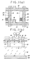
- Fig. 1(a) is a plan view of said photoelectric converting device
- Fig. 1(b) is a cross-sectional veiw thereof along a line A - A′.
- photosensor cells are arranged on an n+-silicon substrate 12, and each photosensor cell is electrically insulated from neighboring photosensor cells by a separating area 13 composed of SiO2, Si3N4 or polysilicon.
- Each photosensor cell is composed in the following manner.
- a p-domain 15 is formed by doping with a p-type impurity such as boron, and an n+-domain 16 is formed thereon by impurity diffusion or ion implantation.
- Said p-domain 15 and n+-domain 16 respectively constitute base and emitter of a bipolar transistor.
- Said electrode 18 faces the p-domain 15 across the oxide laery 17 and receives a pulse voltage to control the potential of said p-domain 15 in floating state.
- an emitter electrode 19 connected to the n+-domain 16, a wiring 20 for releasing a signal from the emitter electrode 19 to the outside, a wiring 21 connected to the electrode 18, an n+-domain 22 of a high impurity concentration formed on the rear face of the n+-silicon substrate 12, and an electrode 23 for biasing the collector of the bipolar transistor.
- the above-explained photoelectric converting device functions in the following manner.
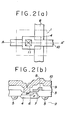
- Fig. 2(a) is a plan veiw of a sensor cell of a semiconductor image pickup device obtained by the method of the present invention for producing a photoelectric converting device not associated with the above-explained drawbacks
- Fig. 2(b) is a cross-sectional view along a line A - A′.
- the semiconductor transistor is composed of a bipolar transistor
- the control electrode is composed of the base
- the main electrode is composed of the emitter thereof.
- Fig. 2(a) 1 indicates a sensor cell.
- a field oxide layer 3 of a thickness of 1 ⁇ m by a LOCOS process.
- an n+-channel stopper 5 Under said field oxide layer 3 there may be formed an n+-channel stopper 5 if necessary, for preventing the transfer of positive holes from the neighboring channel.
- a p-domain 4 constituting a base, of an impurity concentration of 1014/cm3 and a diffusion depth of 0.8 ⁇ m is formed by a self-aligning process utilizing said field oxide layer 3 as a mask.
- the basic dimension (minimum rule) is equal to the length of a side of a contact hole to be explained later, and said p-domain 4 constituting an active area is 3 ⁇ 2 times as large as said basic dimension. Then an insulating layer 7 of a thickness of 500 ⁇ is formed, and a polysilicon electrode 8 of a thickness of 4,000 ⁇ is formed thereon, constituting a gate electrode for the p-domain 4. Said electrode 8 is partially placed on the field oxide layer 3 and has a margin for misalignment.
- n+-domain 6 constituting an emitter, of an impurity concentration of 1019/cm3 and a diffusion depth of 0.3 ⁇ m is formed by self-aligned ion implantation utilizing the filed oxide layer 3 and the electrode 8.
- the silicon substrate 2, p-domain 4 and n+-domain 6 constitute a vertical bipolar transistor with h ff in the order of 1,000.
- a PSG interlayer insulator 9 of a thickness of 7,000 ⁇ is formed, a contact hole 11 is opened, and a metal wiring 10 of a thickness of 8,000 ⁇ is electrically connected to said n+-domain 6.
- the use of LOCOS process in the formation of the field oxide layer 3 provides a flat surface, thus facilitating fine pattern fo rmation in the following steps.
- said field oxide layer 3 is used in the self alignment in the formation of the p-domain 4 and n+-domain 6 to avoid alignment error, thereby obtaining stable characteristics of the aforementioned bipolar transistor.
- the n+-domain 6 is formed by the self-alignment process utilizing the electrode 8, the p-domain 4 constituting the active area can be formed with a minimum necessary area, without unnecessary gate-emitter parasite capacity.
- said electrode 8 can be formed very close to the p-domain 4 constituting the base domain, or the active domain of the transistor, so that various parasite effects resulting from excessive base resistance can be avoided. Also, since the active area, or p-domain 4, can be made minimum, it is possible to reduce the base-collector capacity and to improve the device characteristics.
- a conventional photoetching process may be employed, instead of the LOCOS process, for forming the field insulating layer 3.
- LOCOS process a conventional photoetching process
- the LOCOS process is disadvantageous in obtaining a flat surface, it is free from bird's beaks associated in the LOCOS process and can form the base and emitter with exact dimensions.
- Such embodiment allows to achieve further stabilization of the transistor performance.
- another substrate such as an epitaxial substrate is employed as the silicon substrate 2 for simultaneous formation of an NMOS device etc.
- a further increase in the percentage of aperture can be achieved, in the foregoing embodiments, by forming the sensor cell larger than 5 ⁇ 4 times of the basic dimension.
- the p-domain 4 should be preferably positioned close to the corner of the sensor cell for achieving a higher percentage of aperture.
- the electrode 8 and the metal wiring 10 can be composed of any usual material, such as polysilicon aluminum, an aluminum alloy, a high-melting metal or a silicide.
- the insulating layer 7 may be composed of any usual material such as an oxide or a nitride.
- the method of the foregoing embodiments for producing the photoelectric converting device allows to improve the positional precision of the control electrode area and the main electrode area almost without unnecessary margins through formation thereof by a self-aligning process, thereby reducing the cell size of the sensor cell and providing the photoelectric converting device inexpensively with an improved production yield.
- the foregoing embodiments are advantageously applicable for example to semiconductor image pickup devices requiring a high level of integration.
- a photoelectric converting device in which an accumulated charge is generated in the control electrode area of a transistor and the detection of a light signal is achieved by controlling said accumulated charge.
- Fig. 3(a) is a plan view of a sensor cell of said photoelectric converting device
- Fig. 3(b) is a cross-sectional view along a line A - A′ in Fig. 3(a).
- a sensor cell 101 has a size equal to 10 ⁇ 5 times of the basic dimension (minimum design rule equal to the lateral length a of contact holes for metal wirings 111, 113), and is composed as follows.
- an N-type silicon substrate 102 there are formed an N-type diffused separating layer 103, a P-type diffused base layer 105, a P-type diffused source layer 107, and a P-type diffused drain layer, and said P-type diffused base layer 105 there is formed an N-type diffused emitter layer 108.
- Said N-type diffused emitter layer 108, P-type diffused base layer 105 and N-type silicon substrate 102 constitute an NPN bipolar transistor, while the P-type diffused source layer 107, P-type diffused drain layer 106 and a gate electrode 109 formed across a gate oxide layer 112 constitute a PMOS transistor.
- 111 and 113 are metal wirings.
- the base potential is elevated by the accumulated holes, and is further elevated by a voltage applied across the N-type diffused emitter layer 108 and the N-type silicon substrate 102 constituting the emitter, and a positive voltage applied to the gate electrode 109.
- Said change in base potential is read as a change in the collector current, thus as an electric signal corresponding to the intensity of the incident light (read-out operation).
- the charge accumulated in the P-type diffused base layer 105 can be dissipated through the metal wiring 113 by turning on the aforementioned PMOS transistor (refreshing operation). The above-explained steps of accumulation, read-out refreshing are repeated thereafter.
- the above-explained structure is not suitable for a high level of integration because the area of the sensor cell is increased by the PMOS transistor employed for refreshing operation.
- Fig. 4(a) is a plan view of a sensor cell of a photoelectric converting device in said embodiment of the present invention
- Fig. 4(b) is a cross-sectional view along a line A - A′ in Fig. 4(a).
- the transistor is composed of a bipolar transistor
- the control electrode is composed of base area.
- a sensor cell 114 has a size of 5 ⁇ 4 times of the basic dimension (lateral length b of the contact hole of a metal wiring 123), and is isolated by the LOCOS process as will be explained later, but is reduced to 1/2.5 in area compared to the structure shown in Figs. 3(a) and 3(b).
- the sensor cell 114 is formed in the following manner. At first, on a CZP(100) 1 ⁇ -cm silicon substrate 125, there are formed an N-type embedded diffusion layer 124 of a resistivity of 20 ⁇ /cm2 and a P-epitaxial 115 of an impurity concentration of 1015/cm3 and of a thickness of 3.5 ⁇ m.
- a P-type diffused separation layer 116 and a field oxide layer 117 of a thickness of 1 ⁇ m by the LOCOS process are formed.
- an N-type diffused base layer 118 of a depth of 0.8 ⁇ m, an insulation layer 119 of a thickness of 500 ⁇ composed for example of an oxide layer, and a polysilicon electrode 120 of a thickness of 4,000 ⁇ are formed.
- Said electrode 120 functions as the gating electrode for the N-type diffused base layer 118.
- a P-type diffused emitter layer 121 of a depth of 0.3 ⁇ m is formed by a self-alignment process, and there are then formed an interlayer insulation layer 122 and a metal wiring 123.
- the P-type diffused emitter layer 121, N-type diffused base layer 118 and P-type epitaxial layer 115 constitute a PNP bipolar transistor, and the electrode 120 serves to control the accumulated charge.
- the aforementioned N-type embedded diffusion layer 124, P-type epitaxial layer 115 and N-type diffused base layer 118 constitute an NPN vertical transistor or an N-type JFET serving as a second transistor of the present invention.
- the photo-induced charge accumulated in the N-type diffused base layer 118 can be dissipated through said N-type embedded diffusion layer 124, by a punch through between said layer 124 and the N-type base layer 118 induced by a positive voltage applied to said N-type embedded diffusion layer 124.
- the photoelectric converting device of the present embodiment is further provided with an overflow drain structure.
- Figs. 5(a) and 5(b) show potential status of said embodiment, respectively in a state without photo-induced charge and a state with excessive photo-induced charge.
- Figs. 5(a) and 5(b) there are shown the energe levels 126, 127, 128 and 130 respectively of the P-type diffused emitter layer 121, N-type diffused base layer 118, P-type epitaxial layer 115, and N-type embedded diffusion layer 124.
- the electrons of the photo-induced charge generated in the vicinity of the P-type epitaxial layer 115 are accumulated, through diffusion, in the N-type diffused base layer 118.
- the energy level 127 of the N-type base layer 118 is elevated and becomes substantially equal to that of the P-epitaxial layer 115 as shown in Fig. 5(b), so that the electrons are no longer accumulated but move to the N-type embedded diffusion layer 124.
- the photoelectric converting device of the present embodiment in which the charge accumulated to the N-type diffused base layer 118 is transferred to the N-type embedded diffusion layer 124 by a punch-through induced by a voltage applied to said layer 124, can provide a linear photoelectric conversion characteristic and a satisfactory blooming resistance.
- the LOCOS process employed for forming the field oxide layer 117 may be replaced by a conventional photoetching process.
- an N-type silicon substrate may be employed if desirable instead of P-type.
- the conductive type of the above-explained photoelectric converting device may be totally inverted.
- the boron dopant in the P-type base layer 118 is extracted by thermal treatment into the field oxide layer. A resulting lower concentration at the interface tends to cause channel leak phenomenon, and suitable countermeasure will be required therefor.
- the foregoing embodiments provide a photoelectric converting device which ensures linearity of photoelectric conversion by discharging the charge accumulated in a control electrode area into an embedded area, and which enables a high level of integration and an economical production due to the absence of MOS transistors for refreshing operation.
- the contact holes for the emitter electrode has to be formed by alignment, with an aligner, on the emitter domain after the formation thereof. Consequently, in case of obtaining a high level of integration, for example of 1,000 ⁇ 1,000 pixels, the cell size has to be reduced while the contact hole is maintained at an approximately current size. Consequently the emitter and the base will occupy a larger proportion to the cell, thus practically reducing the potential Vp generated in the base.
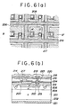
- Fig. 6(a) is a plan view of an embodime nt of the photoelectric converting device of the present invention capable of resolving the above-explained drawbacks
- Fig. 6(b) is a cross-sectional view of a cell thereof along a line B - B′, equivalent portions as those in Figs. 6(a) and 6(b) are represented by same numbers and will not be explained further.
- a p-base domain 209 for accumulating photo-induced charge, and, in said p-base domain 209, there is formed, through a self-aligning process, an n+-emitter domain 215 by impurity diffusion from an n-doped polysilicon electrode 223.
- Such self-aligned formation of the n+-emitter domain 215 from the electrode 223 allows to reduce the emitter size.
- Figs. 7(a) to 7(i) illustrate steps of the method of producing the device of the present embodiment.
- an n+-layer 2 of an impurity concentration of 1 ⁇ 1017 to 1 ⁇ 1020 cm ⁇ 3 for ohmic contact is formed, by the diffusion of P, As or Sb, on the rear face of an n-silicon substrate 201 with an impurity concentration of 1 ⁇ 1015 to 5 ⁇ 1018 cm ⁇ 3.
- an oxide layer 203 for example an SiO2 layer, of a thickness of 3,000 to 7,000 ⁇ is formed by a CVD process on said n+-layer 202.
- the oxide layer 203 is called back coat, and prevents the formation of impurity vapor when the substrate 201 is heat treated.
- n ⁇ -layer 204 an n ⁇ -epitaxial layer (hereinafter called n ⁇ -layer) 204 is formed at a temperature of 1,000°C and a reduced pressure of 120 - 180 Torr, with 1.2 l/min. of SiH2Cl2 (100%) as source gas and 100 cc of PH3 diluted to 20 ppm with H2 as doping gas.
- the monocrystal growth rate is 0.5 ⁇ m/min.
- the layer thickness is 2 to 10 ⁇ m
- the impurity concentration is in a range from 1 ⁇ 1012 to 1016 cm ⁇ 3, preferably from 1012 to 1014 cm ⁇ 3. This state is shown in Fig. 7(b).
- n ⁇ -layer 204 For improving the quality of said n ⁇ -layer 204, it is extremely effective to remove oxygen from the vicinity of the surface of the substrate by a high temperature treatment at 1150-1250°C, and then to generate a number of microdefects in the substrate by a prolonged heat treatment at ca. 800°C, thereby obtaining a substrate with a denuded zone capable of intrinsic gettering.
- a buffer oxide layer 208 of a thickness of 500 to 1,500 ⁇ is formed by pyrogenic oxidation (H2 + O2), wet oxidation (O2 + H2O), steam oxidation (N2 + H2O) or dry oxidation. Pressurized oxidation at 800 to 1,000°C is suitable for obtaining a satisfactory oxide layer without lamination defects.
- the oxide layer 208 is formed for preventing the channeling and surface defects at the formation of the base domain by ion implantation.
- the oxide back-coat layer 203 is completely removed in this step.
- a resist material 210 is coated, and is selectively removed in an area corresponding to the base domain, as shown in Fig. 7(c).
- B+ ions or BF2+ ions generated from BF3 are implanted into the wafer, with a surface concentration in a range from 1 ⁇ 1015 to 5 ⁇ 1018 cm ⁇ 3, preferably from 1 to 20 ⁇ 1016 cm ⁇ 3, and with an amount of ion implantation of 7 ⁇ 1011 to 1 ⁇ 1015 cm ⁇ 2, preferably 1 ⁇ 1012 to 1 ⁇ 1014 cm ⁇ 2.
- the resist 210 is removed, and the p-base domain 9 is formed to a predetermined depth by thermal diffusion at 1,000 - 1,100°C and in a N2 atmosphere, simultaneous with the formation of a thick oxide layer 211 on the surface of the substrate 201. Subsequently said oxide layer 211 is selectively removed in a portion w here the separating area 206 is to be formed, as shown in Fig. 7(d).
- the depth of the p-base domain 209 is for example 0.6 to 1.0 ⁇ m, but said depth and the impurity concentration are determined according to the following concept.
- the impurity concentration of the p-base domain 209 For achieving a higher sensitivity, it is desirable to reduce the impurity concentration of the p-base domain 209, thereby reducing the base-emitter capacity Cbe, which is approximately determined by the following equation: wherein V bi is the emitter-base diffusion potential given by: wherein ⁇ is the dielectric constant of the silicon crystal, N D is the impurity concentration of the emitter, N A is that of the base adjacent to the emitter, n i is the actual carrier concentration, Ae is the area of the base domain, k is Boltzman constant, T is the absolute temperature, and q is the unit charge.
- a smaller N A will reduce the value of Cbe and increase the sensitivity, but is so selected as not to be excessively small, since an excessively small value of N A will render the base domain completely deficient in its operating state and bring the same to a punch-through state.
- the base domain 209 can also be formed by depositing BSG on the wafer and diffusing the impurity B into a predetermined depth by thermal diffusion at 1,100 - 1,200°C.
- an impurity n+ is diffused for forming the separating area 206 with a concentration of 1017 - 1021 cm ⁇ 3 either by diffusion from POCl3 or by ion implantation.
- a satisfactory result could be experimentally obtained by the process with POCl3, with a furnace temperature of 850 - 1,000°C, a flow rate of 50 - 200cc/min. of the carrier gas for POCl3 bubbling, and a process time of 10 - 40 minutes.
- a thick oxide layer 212 is formed by oxidation on the substrate 201. Subsequently the oxide layer 212 is selectively removed in the areas where the capacitor electrode and the emitter are to be formed, and a gate oxide layer 207 and an oxide layer 207′ of a thickness of 100 - 1,000 ⁇ are forced respectively in thus obtained apertures, as shown in Fig. 7(e).
- As-doped polysilicon layer is deposited by CVD process from (N2 + SiH4 + AsH3) gas or (H2 + SiH4 + AsH3) gas, with a thickness of 2,000 to 7,000 ⁇ , at a deposition temperature of 550 - 900°C.
- CVD process from (N2 + SiH4 + AsH3) gas or (H2 + SiH4 + AsH3) gas, with a thickness of 2,000 to 7,000 ⁇ , at a deposition temperature of 550 - 900°C.
- non-doped polysilicon by CVD process and then to dope said polysilicon with As or P.
- the polysilicon layer thus deposited is then photolithographically etched off to obtain the polysilicon layer 214 constituting the capacitor electrode, as shown in Fig. 7(f).
- thermal oxide layer 224 of a thickness of 100 - 1,000 ⁇ serving as the interlayer insulating layer, as shown in Fig. 7(g).
- a contact hole 222 is formed in a position in the p-base domain 209 where the emitter domain is to be formed, as shown in Fig. 7(h).
- As-doped polysilicon layer is deposited by CVD process from (N2 + SiH4 + AsH3) gas or (H2 + SiH4 + AsH3) gas, with a thickness of 2,000 to 7,000 ⁇ , at a deposition temperature of 550 - 900°C.
- CVD process from (N2 + SiH4 + AsH3) gas or (H2 + SiH4 + AsH3) gas, with a thickness of 2,000 to 7,000 ⁇ , at a deposition temperature of 550 - 900°C.
- the polysilicon layer thus deposited is then photolithographically etched off to form a polysilicon electrode 225, and a thermal treatment is effected to diffuse As, contained in said polysilicon electrode 225, into the p-base domain 209, thereby forming an n+-emitter domain 215 by self-alignment, as shown in Fig. 7(i).
- a PSG layer or a SiO2 layer 216 of a thickness of 3,000 - 7,000 ⁇ is formed by a gas CVD process explained above, and a contact hole is opened on the polysilicon layer 214 through a masking step and an etching step.
- a metal electrode 217 for example of Al, Al-Si or Al-Cu-Si, is deposited by vacuum evaporation or sputtering in said contact hole, as shown in Fig. 7(j).
- an insulating interlayer 218, for example a PSG layer or a SiO2 layer, of a thickness of 3,000 - 9,000 ⁇ is deposited by a CVD process.
- a contact hole is opened on the emitter domain 215 through a masking step and an etching step, a metal electrode 219, for example of Al, Al-Si or Al-Cu-Si is formed therein, as shown in Fig. 7(k).
- a passivation layer 220 composed for example of a PSG layer or a Si3N4 layer is formed by a CVD process, and a metal electrode 221, composed for example of Al, Al-Si or Au is formed on the rear face of the wafer to obtain the photoelectric converting device shown in Figs. 6(a) and 6(b).
- the separating area is composed of an n+-semiconductor, but it may naturally replaced by a p+-semiconductor in case of a PNP bipolar transistor.
- the photoelectric converting device of the present embodiment is capable of reducing the area of a main electrode, for example the emitter, by the formation in a control electrode domain through a self-alignment, thereby reducing the area of said control electrode.
- a higher level of integration can be achieved without a loss in the photo-induced potential, since a reduction in the photo-induced charge Q caused by the cell size reduction can be wholly or almost wholly compensated by the reduction of the size of the control electrode area.
Landscapes
- Engineering & Computer Science (AREA)
- Physics & Mathematics (AREA)
- Power Engineering (AREA)
- Computer Hardware Design (AREA)
- Electromagnetism (AREA)
- Condensed Matter Physics & Semiconductors (AREA)
- General Physics & Mathematics (AREA)
- Microelectronics & Electronic Packaging (AREA)
- Nanotechnology (AREA)
- Materials Engineering (AREA)
- Chemical & Material Sciences (AREA)
- Solid State Image Pick-Up Elements (AREA)
- Light Receiving Elements (AREA)
- Transforming Light Signals Into Electric Signals (AREA)
- Photovoltaic Devices (AREA)
Abstract
Description
- The present invention relates to a photoelectric converting device, more particularly a photoelectric converting device obtained by forming an electrode across an insulating layer on a control electrode area of a semiconductor transistor, and a method for producing the same.
- In conventional semiconductor image pickup devices, the cell size of the sensor portion constituting a separate device cannot be considered sufficiently small in comparison with the advanced degree of integration of the driving circuit portion. For example, in contrast to the usual cell size of about 70 µm² in a 256K DRAM, that of a semiconductor image pickup device for example of 500 × 500 pixels is as several times as large as 200 to 300 µm². An increase in the cell size increases the chip area and therefore reduces the number of chips per wafer. Also in comparison with usual digital logic circuit devices, semiconductor image pickup devices are associated with much lower production yields because they have to satisfy optical and analog characteristics. For these reasons the cost per chip of the sensor portion is inevitably higher than that of DRAM or similar devices.
- The reduction of cell size can be achieved either by a scale-down method, in which dimensions are proportionally reduced or by a cell improvement method in which the number of cell constituting components is reduced.
- The cell size has been reduced year after year with the progress of microintegration technology, but the rate of size reduction is in average in the range 0.88 times per year. Thus a drastic size reduction cannot be expected in the former method. More detailedly, though a size reduction results in a reduction in the chip area and thus an increase in the number of chips per wafer, the production yield is lowered due to increased difficulty of process control. Consequently the number of defectless chips per wafer will show a peak at a certain cell dimension.
- On the other hand, the latter method can achieve a drastic size reduction. For example, in case of a random access memory, a memory unit originally composed of 6 to 8 transistors in now simplified to a transistor and a capacitor.
- The latter cell improvement method is also effective in the field of semiconductor image pickup devices. For example charge-coupled image pickup devices (CCD) are now superior to MOS image pickup devices in simplicity and integration, by isolating each carrier accumulating portion not by a mechanical structure but by an electrically formed potential well. Also the charge transfer portion does not require sources and drains in the MOS structure and can therefore achieve a higher degree of integration. Though CCD's can achieve a higher level of integration in comparison with MOS devices, they are disadvantageous in production yield, because, in CCD's, a defect in the charge transfer portion affects the image information of an entire corresponding line. Also defects in the substrate cannot be tolerated because the information transfer is conducted not by metal wirings but by the interior of the substrate itself, and these facts deteriorate the production yield and raise the production cost. Under such situation, CCD's an MOS devices are now competing each other in the field of semiconductor image pickup devices.
- An object of the present invention is to reduce the cell size of a photoelectric converting device through an improvement in the cell structure thereof.
- Another object of the present invention is to provide a method for producing a photoelectric converting device with an improved precisio n of the control electrode domain and the main electrode domain in the cells thereof.
- Still another object of the present invention is to provide a photoelectric converting device with a reduced cell size achieved by economizing the area of a transistor refreshing the accumulated charge in each photoelectric converting cell.
- Still another object of the present invention is to provide a photoelectric converting device with a reduced cell size achieved by reducing the area of a control electrode area in each photoelectric converting cell.
-
- Fig. 1(a) is a plan veiw of a photoelectric converting device;
- Fig. 1(b) is a cross-sectional veiw along a line A - A′ in Fig. 1(a);
- Fig. 2(a) is a schematic view of a sensor cell of a semiconductor image pickup device obtained according to the process for producing a photoelectric converting device of the present invention;
- Fig. 2(b) is a cross-sectional view along a line A - A′ in Fig. 2(a);
- Figs. 3(a) and 3(b) are schematic views of a sensor cell of a conventional photoelectric converting device;
- Figs. 4(a) and 4(b) are schematic veiws of a sensor cell of a photoelectric converting device of the present invention;
- Figs. 5(a) and 5(b) are charts showing the potential characteristics of said photoelectric converting device;
- Fig. 6(a) is a plan veiw of a photoelectric converting device embodying the present invention;
- Fig. 6(b) is a cross-sectional view of a cell along a line B - B′ in Fig. 6(a); and
- Figs. 7(a) to 7(k) are views showing the steps of the method of producing the photoelectric converting device in said embodiment.
- Now, the present invention will be clarified in detail by an embodiment thereof shown in the attached drawdings.
- A semiconductor image pickup device of a high level of integration can be formed with the photoelectric converting device disclosed in the Japanese Patent Laid-open No. 12759/1985.
- Fig. 1(a) is a plan view of said photoelectric converting device, and Fig. 1(b) is a cross-sectional veiw thereof along a line A - A′.
- In Figs. 1(a) and 1(b), photosensor cells are arranged on an n⁺-
silicon substrate 12, and each photosensor cell is electrically insulated from neighboring photosensor cells by a separatingarea 13 composed of SiO₂, Si₃N₄ or polysilicon. - Each photosensor cell is composed in the following manner.
- On an n⁻-
domain 14 of a low impurity concentration formed for example by epitaxial growth, a p-domain 15 is formed by doping with a p-type impurity such as boron, and an n⁺-domain 16 is formed thereon by impurity diffusion or ion implantation. Said p-domain 15 and n⁺-domain 16 respectively constitute base and emitter of a bipolar transistor. - On the p-
domain 15 of the above-explained structure and on aseparating area 13, there is formed anoxide layer 17 on which formed is anelectrode 18 of a predetermined area. Saidelectrode 18 faces the p-domain 15 across theoxide laery 17 and receives a pulse voltage to control the potential of said p-domain 15 in floating state. There are further provided anemitter electrode 19 connected to the n⁺-domain 16, awiring 20 for releasing a signal from theemitter electrode 19 to the outside, awiring 21 connected to theelectrode 18, an n⁺-domain 22 of a high impurity concentration formed on the rear face of the n⁺-silicon substrate 12, and anelectrode 23 for biasing the collector of the bipolar transistor. - The above-explained photoelectric converting device functions in the following manner.
- In response to
incident light 24, electron-hole pairs are generated in the s emiconductor in proportion to the intensity of incident light. The electrons elude to the positively biased n⁺-silicon substrate 12, but the positive holes are accumulated in the p-domain 15 (accumulating operation). The base potential is elevated by the accumulated positive holes. The base potential is further elevated by a voltage applied across the n⁺-domain 16 constituting the emitter and the n⁺-silicon substrate 12 constituting the collector, and by a positive voltage applied to theelectrode 18. This potential change is read as the collector current, constituting an electric signal corresponding to the intensity of incident light (read-out operation). The charge accumulated in the p-domain 15 can be eliminated by grounding theemitter electrode 19 and applying a positive pulse to theelectrode 18. Said positive voltage biases the p-domain 15 in forward direction with respect to the n⁺-domain 16, thereby discharging the accumulated charge (refreshing operation). The above-mentioned steps of accumulation, read-out and refreshing are repeated thereafter. - However the above-explained photoelectric converting device, when applied to a semiconductor image pickup device of 500 × 500 pixels, requires a cell size of about 200 µm² and is not adequate for achieving a high level of integration.
- Fig. 2(a) is a plan veiw of a sensor cell of a semiconductor image pickup device obtained by the method of the present invention for producing a photoelectric converting device not associated with the above-explained drawbacks, and Fig. 2(b) is a cross-sectional view along a line A - A′. In the present embodiment the semiconductor transistor is composed of a bipolar transistor, the control electrode is composed of the base and the main electrode is composed of the emitter thereof.
- In Fig. 2(a), 1 indicates a sensor cell. On a CZN(100) 10 Ω-cm silicon substrate 2, there is formed a
field oxide layer 3 of a thickness of 1 µm by a LOCOS process. Under saidfield oxide layer 3 there may be formed an n⁺-channel stopper 5 if necessary, for preventing the transfer of positive holes from the neighboring channel. Then a p-domain 4, constituting a base, of an impurity concentration of 10¹⁴/cm³ and a diffusion depth of 0.8 µm is formed by a self-aligning process utilizing saidfield oxide layer 3 as a mask. The basic dimension (minimum rule) is equal to the length of a side of a contact hole to be explained later, and said p-domain 4 constituting an active area is 3 × 2 times as large as said basic dimension. Then an insulatinglayer 7 of a thickness of 500 Å is formed, and apolysilicon electrode 8 of a thickness of 4,000 Å is formed thereon, constituting a gate electrode for the p-domain 4. Saidelectrode 8 is partially placed on thefield oxide layer 3 and has a margin for misalignment. Then formed is an n⁺-domain 6, constituting an emitter, of an impurity concentration of 10¹⁹/cm³ and a diffusion depth of 0.3 µm is formed by self-aligned ion implantation utilizing the filedoxide layer 3 and theelectrode 8. The silicon substrate 2, p-domain 4 and n⁺-domain 6 constitute a vertical bipolar transistor with h ff in the order of 1,000. Then aPSG interlayer insulator 9 of a thickness of 7,000 Å is formed, a contact hole 11 is opened, and ametal wiring 10 of a thickness of 8,000 Å is electrically connected to said n⁺-domain 6. - In the present embodiment, the cell dimension for a basic dimension of 2 µ is 10 × 8 = 80 µm², which is comparable to the cell area of 70 µm² of 256K DRAM of 2 µ design rule, and which is almost 1/3 of the cell area of 200 to 300 µm² in the conventional semiconductor image pickup devices. Also the percentage of aperture excluding the
electrode 8 and themetal wiring 10 is 51 % and is practically acceptable. - In the present embodiment, the use of LOCOS process in the formation of the
field oxide layer 3 provides a flat surface, thus facilitating fine pattern fo rmation in the following steps. Also saidfield oxide layer 3 is used in the self alignment in the formation of the p-domain 4 and n⁺-domain 6 to avoid alignment error, thereby obtaining stable characteristics of the aforementioned bipolar transistor. Also since the n⁺-domain 6 is formed by the self-alignment process utilizing theelectrode 8, the p-domain 4 constituting the active area can be formed with a minimum necessary area, without unnecessary gate-emitter parasite capacity. Also saidelectrode 8 can be formed very close to the p-domain 4 constituting the base domain, or the active domain of the transistor, so that various parasite effects resulting from excessive base resistance can be avoided. Also, since the active area, or p-domain 4, can be made minimum, it is possible to reduce the base-collector capacity and to improve the device characteristics. - In another embodiment of the present invention, a conventional photoetching process may be employed, instead of the LOCOS process, for forming the
field insulating layer 3. Though such process is disadvantageous in obtaining a flat surface, it is free from bird's beaks associated in the LOCOS process and can form the base and emitter with exact dimensions. Thus such embodiment allows to achieve further stabilization of the transistor performance. - Also as another embodiment, another substrate such as an epitaxial substrate is employed as the silicon substrate 2 for simultaneous formation of an NMOS device etc.
- A further increase in the percentage of aperture can be achieved, in the foregoing embodiments, by forming the sensor cell larger than 5 × 4 times of the basic dimension. In this case, the p-
domain 4 should be preferably positioned close to the corner of the sensor cell for achieving a higher percentage of aperture. - The
electrode 8 and themetal wiring 10 can be composed of any usual material, such as polysilicon aluminum, an aluminum alloy, a high-melting metal or a silicide. Also the insulatinglayer 7 may be composed of any usual material such as an oxide or a nitride. - As explained in the foregoing, the method of the foregoing embodiments for producing the photoelectric converting device allows to improve the positional precision of the control electrode area and the main electrode area almost without unnecessary margins through formation thereof by a self-aligning process, thereby reducing the cell size of the sensor cell and providing the photoelectric converting device inexpensively with an improved production yield. The foregoing embodiments are advantageously applicable for example to semiconductor image pickup devices requiring a high level of integration.
- For the purpose of improving the production yield of semiconductor image pickup devices of CCD type, there can be employed a photoelectric converting device in which an accumulated charge is generated in the control electrode area of a transistor and the detection of a light signal is achieved by controlling said accumulated charge.
- In the following such photoelectric converting device will be explained.
- Fig. 3(a) is a plan view of a sensor cell of said photoelectric converting device, and Fig. 3(b) is a cross-sectional view along a line A - A′ in Fig. 3(a).
- In Fig. 3(a), a
sensor cell 101 has a size equal to 10 × 5 times of the basic dimension (minimum design rule equal to the lateral length a of contact holes for metal wirings 111, 113), and is composed as follows. On an N-type silicon substrate 102, there are formed an N-type diffusedseparating layer 103, a P-type diffusedbase layer 105, a P-type diffusedsource layer 107, and a P-type diffused drain layer, and said P-type diffusedbase layer 105 there is formed an N-type diffusedemitter layer 108. Said N-type diffusedemitter layer 108, P-type diffusedbase layer 105 and N-type silicon substrate 102 constitute an NPN bipolar transistor, while the P-type diffusedsource layer 107, P-type diffuseddrain layer 106 and agate electrode 109 formed across agate oxide layer 112 constitute a PMOS transistor. 111 and 113 are metal wirings. - In the following there will be explained the function of the above-explained photoelectric converting device.
- In response to incident light, electron-positive hole pairs are generated in the semiconductor in proportion to the intensity of the incident light. The electrons elude from the positively biased N-
type silicon substrate 102, but the positive holes are accumulated in the P-type diffused base layer 105 (accumulating operation). - The base potential is elevated by the accumulated holes, and is further elevated by a voltage applied across the N-type diffused
emitter layer 108 and the N-type silicon substrate 102 constituting the emitter, and a positive voltage applied to thegate electrode 109. Said change in base potential is read as a change in the collector current, thus as an electric signal corresponding to the intensity of the incident light (read-out operation). Also the charge accumulated in the P-type diffusedbase layer 105 can be dissipated through themetal wiring 113 by turning on the aforementioned PMOS transistor (refreshing operation). The above-explained steps of accumulation, read-out refreshing are repeated thereafter. - The above-explained structure is not suitable for a high level of integration because the area of the sensor cell is increased by the PMOS transistor employed for refreshing operation.
- For achieving a high level of integration, there may be employed a refreshing method of forming an electrode on the
gate oxide layer 112 on the P-type diffusedbase layer 105, instead of said PMOS transistor, and applying a voltage to said electrode to dissipate the accumulate charge. However this method has a drawback that the linearity of photoelectric conversion is affected because the base potential is not clearly fixed. - In the following there will be explained another embodiment of the present invention, which resolves the above-explained drawbacks of the prior technology, while making reference to the attached drawings.
- Fig. 4(a) is a plan view of a sensor cell of a photoelectric converting device in said embodiment of the present invention, and Fig. 4(b) is a cross-sectional view along a line A - A′ in Fig. 4(a). In the present embodiment the transistor is composed of a bipolar transistor, and the control electrode is composed of base area.
- In Fig. 4(a) a sensor cell 114 has a size of 5 × 4 times of the basic dimension (lateral length b of the contact hole of a metal wiring 123), and is isolated by the LOCOS process as will be explained later, but is reduced to 1/2.5 in area compared to the structure shown in Figs. 3(a) and 3(b). The sensor cell 114 is formed in the following manner. At first, on a CZP(100) 1 Ω-cm silicon substrate 125, there are formed an N-type embedded diffusion layer 124 of a resistivity of 20 Ω/cm² and a P-epitaxial 115 of an impurity concentration of 10¹⁵/cm³ and of a thickness of 3.5 µm. Then a P-type diffused separation layer 116 and a field oxide layer 117 of a thickness of 1 µm by the LOCOS process. Subsequently an N-type diffused base layer 118 of a depth of 0.8 µm, an insulation layer 119 of a thickness of 500 Å composed for example of an oxide layer, and a polysilicon electrode 120 of a thickness of 4,000 Å are formed. Said electrode 120 functions as the gating electrode for the N-type diffused base layer 118. Subsequently a P-type diffused emitter layer 121 of a depth of 0.3 µm is formed by a self-alignment process, and there are then formed an interlayer insulation layer 122 and a metal wiring 123. The P-type diffused emitter layer 121, N-type diffused base layer 118 and P-type epitaxial layer 115 constitute a PNP bipolar transistor, and the electrode 120 serves to control the accumulated charge.
- The aforementioned N-type embedded diffusion layer 124, P-type epitaxial layer 115 and N-type diffused base layer 118 constitute an NPN vertical transistor or an N-type JFET serving as a second transistor of the present invention. The photo-induced charge accumulated in the N-type diffused base layer 118 can be dissipated through said N-type embedded diffusion layer 124, by a punch through between said layer 124 and the N-type base layer 118 induced by a positive voltage applied to said N-type embedded diffusion layer 124.
- The photoelectric converting device of the present embodiment, not requiring a MOS transistor for dissipating the charge accumulated in the N-type diffused base layer, can reduce the cell size to 10 × 8 = 80 µm² for a basic dimension of 2 µm, which is comparable to the cell area of 70 µm² of a 256 K DRAM with a same basic dimension.
- The photoelectric converting device of the present embodiment is further provided with an overflow drain structure.
- Figs. 5(a) and 5(b) show potential status of said embodiment, respectively in a state without photo-induced charge and a state with excessive photo-induced charge.
- In Figs. 5(a) and 5(b) there are shown the
energe levels - The electrons of the photo-induced charge generated in the vicinity of the P-type epitaxial layer 115 are accumulated, through diffusion, in the N-type diffused base layer 118. When the electrons are accumulated, the
energy level 127 of the N-type base layer 118 is elevated and becomes substantially equal to that of the P-epitaxial layer 115 as shown in Fig. 5(b), so that the electrons are no longer accumulated but move to the N-type embedded diffusion layer 124. - The photoelectric converting device of the present embodiment, in which the charge accumulated to the N-type diffused base layer 118 is transferred to the N-type embedded diffusion layer 124 by a punch-through induced by a voltage applied to said layer 124, can provide a linear photoelectric conversion characteristic and a satisfactory blooming resistance.
- In the present embodiment the LOCOS process employed for forming the field oxide layer 117 may be replaced by a conventional photoetching process. Also an N-type silicon substrate may be employed if desirable instead of P-type.
- As another embodiment of the present invention, the conductive type of the above-explained photoelectric converting device may be totally inverted. In this case, after the formation of the base domain, the boron dopant in the P-type base layer 118 is extracted by thermal treatment into the field oxide layer. A resulting lower concentration at the interface tends to cause channel leak phenomenon, and suitable countermeasure will be required therefor.
- As explained detailedly above, the foregoing embodiments provide a photoelectric converting device which ensures linearity of photoelectric conversion by discharging the charge accumulated in a control electrode area into an embedded area, and which enables a high level of integration and an economical production due to the absence of MOS transistors for refreshing operation.
- Next, in a type of photoelectric converting device, the contact holes for the emitter electrode has to be formed by alignment, with an aligner, on the emitter domain after the formation thereof. Consequently, in case of obtaining a high level of integration, for example of 1,000 × 1,000 pixels, the cell size has to be reduced while the contact hole is maintained at an approximately current size. Consequently the emitter and the base will occupy a larger proportion to the cell, thus practically reducing the potential Vp generated in the base.
- Fig. 6(a) is a plan view of an embodime nt of the photoelectric converting device of the present invention capable of resolving the above-explained drawbacks, and Fig. 6(b) is a cross-sectional view of a cell thereof along a line B - B′, equivalent portions as those in Figs. 6(a) and 6(b) are represented by same numbers and will not be explained further.
- Referring to Figs. 6(a) and 6(b), in an n-
epitaxial layer 4 there is formed a p-base domain 209 for accumulating photo-induced charge, and, in said p-base domain 209, there is formed, through a self-aligning process, an n⁺-emitter domain 215 by impurity diffusion from an n-dopedpolysilicon electrode 223. - Such self-aligned formation of the n⁺-
emitter domain 215 from theelectrode 223 allows to reduce the emitter size. - Figs. 7(a) to 7(i) illustrate steps of the method of producing the device of the present embodiment.
- At first, as shown in Fig. 7(a), an n⁺-layer 2 of an impurity concentration of 1 × 10¹⁷ to 1 × 10²⁰ cm⁻³ for ohmic contact is formed, by the diffusion of P, As or Sb, on the rear face of an n-
silicon substrate 201 with an impurity concentration of 1 × 10¹⁵ to 5 × 10¹⁸ cm⁻³. Subsequently anoxide layer 203, for example an SiO₂ layer, of a thickness of 3,000 to 7,000 Å is formed by a CVD process on said n⁺-layer 202. - The
oxide layer 203 is called back coat, and prevents the formation of impurity vapor when thesubstrate 201 is heat treated. - Then the surface of the
substrate 201 is etched for ca. 1.5 minutes at 1,000°C and with 2 ℓ/min. of Hcl and 60 ℓ/min. of H₂, and an n⁻-epitaxial layer (hereinafter called n⁻-layer) 204 is formed at a temperature of 1,000°C and a reduced pressure of 120 - 180 Torr, with 1.2 ℓ/min. of SiH₂Cl₂ (100%) as source gas and 100 cc of PH₃ diluted to 20 ppm with H₂ as doping gas. The monocrystal growth rate is 0.5 µm/min., the layer thickness is 2 to 10 µm, and the impurity concentration is in a range from 1 × 10¹² to 10¹⁶ cm⁻³, preferably from 10¹² to 10¹⁴ cm⁻³. This state is shown in Fig. 7(b). - For improving the quality of said n⁻-
layer 204, it is extremely effective to remove oxygen from the vicinity of the surface of the substrate by a high temperature treatment at 1150-1250°C, and then to generate a number of microdefects in the substrate by a prolonged heat treatment at ca. 800°C, thereby obtaining a substrate with a denuded zone capable of intrinsic gettering. - Subsequently, on the n⁻-
layer 204, abuffer oxide layer 208 of a thickness of 500 to 1,500 Å is formed by pyrogenic oxidation (H₂ + O₂), wet oxidation (O₂ + H₂O), steam oxidation (N₂ + H₂O) or dry oxidation. Pressurized oxidation at 800 to 1,000°C is suitable for obtaining a satisfactory oxide layer without lamination defects. - The
oxide layer 208 is formed for preventing the channeling and surface defects at the formation of the base domain by ion implantation. The oxide back-coat layer 203 is completely removed in this step. - Then a resist
material 210 is coated, and is selectively removed in an area corresponding to the base domain, as shown in Fig. 7(c). - Subsequently B⁺ ions or BF₂⁺ ions generated from BF₃ are implanted into the wafer, with a surface concentration in a range from 1 × 10¹⁵ to 5 × 10¹⁸ cm⁻³, preferably from 1 to 20 × 10¹⁶ cm⁻³, and with an amount of ion implantation of 7 × 10¹¹ to 1 × 10¹⁵ cm⁻², preferably 1 × 10¹² to 1 × 10¹⁴ cm⁻².
- Thereafter the resist 210 is removed, and the p-
base domain 9 is formed to a predetermined depth by thermal diffusion at 1,000 - 1,100°C and in a N₂ atmosphere, simultaneous with the formation of athick oxide layer 211 on the surface of thesubstrate 201. Subsequently saidoxide layer 211 is selectively removed in a portion w here the separatingarea 206 is to be formed, as shown in Fig. 7(d). - The depth of the p-
base domain 209 is for example 0.6 to 1.0 µm, but said depth and the impurity concentration are determined according to the following concept. - For achieving a higher sensitivity, it is desirable to reduce the impurity concentration of the p-
base domain 209, thereby reducing the base-emitter capacity Cbe, which is approximately determined by the following equation:

- The
base domain 209 can also be formed by depositing BSG on the wafer and diffusing the impurity B into a predetermined depth by thermal diffusion at 1,100 - 1,200°C. - Subsequently an impurity n⁺ is diffused for forming the separating
area 206 with a concentration of 10¹⁷ - 10²¹ cm⁻³ either by diffusion from POCl₃ or by ion implantation. A satisfactory result could be experimentally obtained by the process with POCl₃, with a furnace temperature of 850 - 1,000°C, a flow rate of 50 - 200cc/min. of the carrier gas for POCl₃ bubbling, and a process time of 10 - 40 minutes. - After the formation of the separating
area 206 and thebase domain 209 in this manner, athick oxide layer 212 is formed by oxidation on thesubstrate 201. Subsequently theoxide layer 212 is selectively removed in the areas where the capacitor electrode and the emitter are to be formed, and agate oxide layer 207 and anoxide layer 207′ of a thickness of 100 - 1,000 Å are forced respectively in thus obtained apertures, as shown in Fig. 7(e). - Then as As-doped polysilicon layer is deposited by CVD process from (N₂ + SiH₄ + AsH₃) gas or (H₂ + SiH₄ + AsH₃) gas, with a thickness of 2,000 to 7,000 Å, at a deposition temperature of 550 - 900°C. Naturally it is possible to deposite non-doped polysilicon by CVD process and then to dope said polysilicon with As or P. The polysilicon layer thus deposited is then photolithographically etched off to obtain the
polysilicon layer 214 constituting the capacitor electrode, as shown in Fig. 7(f). - On the
polysilicon layer 214 and theoxide layer 212, there is formed athermal oxide layer 224 of a thickness of 100 - 1,000 Å serving as the interlayer insulating layer, as shown in Fig. 7(g). - Then a
contact hole 222 is formed in a position in the p-base domain 209 where the emitter domain is to be formed, as shown in Fig. 7(h). - Subsequently as As-doped polysilicon layer is deposited by CVD process from (N₂ + SiH₄ + AsH₃) gas or (H₂ + SiH₄ + AsH₃) gas, with a thickness of 2,000 to 7,000 Å, at a deposition temperature of 550 - 900°C. Naturally it is possible to deposite non-doped polysilicon by CVD process and then to dope said polysilicon with As. The polysilicon layer thus deposited is then photolithographically etched off to form a
polysilicon electrode 225, and a thermal treatment is effected to diffuse As, contained in saidpolysilicon electrode 225, into the p-base domain 209, thereby forming an n⁺-emitter domain 215 by self-alignment, as shown in Fig. 7(i). - It is also possible to form the
polysilicon layer 214 afte r the formation of theemitter area 215, but the thermal treatment at the formation of the insulatinglayer 224 after the thermal diffusion for emitter formation further increases the thermal diffusion of theemitter domain 215, thus deteriorating the control characteristics of the transistor. It is therefore desirable to form thepolysilicon electrode 225 and theemitter domain 215, after the formation of thepolysilicon layer 214. - Subsequently a PSG layer or a
SiO₂ layer 216 of a thickness of 3,000 - 7,000 Å is formed by a gas CVD process explained above, and a contact hole is opened on thepolysilicon layer 214 through a masking step and an etching step. Ametal electrode 217, for example of Al, Al-Si or Al-Cu-Si, is deposited by vacuum evaporation or sputtering in said contact hole, as shown in Fig. 7(j). - Then an insulating
interlayer 218, for example a PSG layer or a SiO₂ layer, of a thickness of 3,000 - 9,000 Å is deposited by a CVD process. A contact hole is opened on theemitter domain 215 through a masking step and an etching step, ametal electrode 219, for example of Al, Al-Si or Al-Cu-Si is formed therein, as shown in Fig. 7(k). - Finally a
passivation layer 220, composed for example of a PSG layer or a Si₃N₄ layer is formed by a CVD process, and ametal electrode 221, composed for example of Al, Al-Si or Au is formed on the rear face of the wafer to obtain the photoelectric converting device shown in Figs. 6(a) and 6(b). - In the foregoing explanation the separating area is composed of an n⁺-semiconductor, but it may naturally replaced by a p⁺-semiconductor in case of a PNP bipolar transistor.
- As detailedly explained above, the photoelectric converting device of the present embodiment is capable of reducing the area of a main electrode, for example the emitter, by the formation in a control electrode domain through a self-alignment, thereby reducing the area of said control electrode. Thus a higher level of integration can be achieved without a loss in the photo-induced potential, since a reduction in the photo-induced charge Q caused by the cell size reduction can be wholly or almost wholly compensated by the reduction of the size of the control electrode area.
Claims (5)
forming a field insulating layer on a semiconductor substrate;
forming a control electrode domain by a self-alignment process utilizing said field insulating layer as a mask;
forming an insulating layer on said control electrode domain and forming an electrode thereon; and
forming a main electrode domain by a self-alignment process utilizing said field insulating layer and said electrode as a mask.
an embedded domain of a conductive type formed on a semiconductor substrate; and
a semiconductor domain formed on said embedded domain and having a conductive type opposite to that of said embedded domain;
wherein said control electrode domain of a conductive type same as that of said embedded domain is formed in said semiconductor domain.
wherein one of said main electrode domains is formed in said control electrode domain by a self-alignment process utilizing a main electrode connected to said main electrode domain.
Applications Claiming Priority (6)
| Application Number | Priority Date | Filing Date | Title |
|---|---|---|---|
| JP23282/86 | 1986-02-04 | ||
| JP61023282A JPS62179760A (en) | 1986-02-04 | 1986-02-04 | Manufacture of photoelectric conversion device |
| JP125937/86 | 1986-06-02 | ||
| JP61125937A JPH0691234B2 (en) | 1986-06-02 | 1986-06-02 | Photoelectric conversion device |
| JP61156266A JPS6313369A (en) | 1986-07-04 | 1986-07-04 | Photo electric conversion device |
| JP156266/86 | 1986-07-04 |
Publications (3)
| Publication Number | Publication Date |
|---|---|
| EP0232148A2 true EP0232148A2 (en) | 1987-08-12 |
| EP0232148A3 EP0232148A3 (en) | 1988-04-20 |
| EP0232148B1 EP0232148B1 (en) | 1994-08-03 |
Family
ID=27284192
Family Applications (1)
| Application Number | Title | Priority Date | Filing Date |
|---|---|---|---|
| EP87300853A Expired - Lifetime EP0232148B1 (en) | 1986-02-04 | 1987-01-30 | Photoelectric converting device and method for producing the same |
Country Status (4)
| Country | Link |
|---|---|
| US (1) | US5089425A (en) |
| EP (1) | EP0232148B1 (en) |
| AT (1) | ATE109593T1 (en) |
| DE (1) | DE3750300T2 (en) |
Families Citing this family (4)
| Publication number | Priority date | Publication date | Assignee | Title |
|---|---|---|---|---|
| JP3061891B2 (en) * | 1991-06-21 | 2000-07-10 | キヤノン株式会社 | Method for manufacturing semiconductor device |
| US5416344A (en) * | 1992-07-29 | 1995-05-16 | Nikon Corporation | Solid state imaging device and method for producing the same |
| US5552619A (en) * | 1995-05-10 | 1996-09-03 | National Semiconductor Corporation | Capacitor coupled contactless imager with high resolution and wide dynamic range |
| JP2004134514A (en) * | 2002-10-09 | 2004-04-30 | Canon Inc | Rear face incident imaging sensor |
Citations (5)
| Publication number | Priority date | Publication date | Assignee | Title |
|---|---|---|---|---|
| US3624428A (en) * | 1970-03-20 | 1971-11-30 | Rca Corp | Electric signal processing circuit employing capacitively scanned phototransistor array |
| US3816769A (en) * | 1969-12-17 | 1974-06-11 | Integrated Photomatrix Ltd | Method and circuit element for the selective charging of a semiconductor diffusion region |
| US4242695A (en) * | 1978-01-27 | 1980-12-30 | Hitachi, Ltd. | Low dark current photo-semiconductor device |
| EP0022388A1 (en) * | 1979-07-10 | 1981-01-14 | Thomson-Csf | Method of making a vertical DMOS type field effect transistor |
| JPS60142561A (en) * | 1983-12-28 | 1985-07-27 | Matsushita Electric Ind Co Ltd | Manufacture of image pick-up device |
Family Cites Families (8)
| Publication number | Priority date | Publication date | Assignee | Title |
|---|---|---|---|---|
| US3533158A (en) * | 1967-10-30 | 1970-10-13 | Hughes Aircraft Co | Method of utilizing an ion beam to form custom circuits |
| JPS49105490A (en) * | 1973-02-07 | 1974-10-05 | ||
| NL7308240A (en) * | 1973-06-14 | 1974-12-17 | ||
| JPS5795769A (en) * | 1980-12-05 | 1982-06-14 | Fuji Photo Film Co Ltd | Semiconductor image pickup device |
| US4686554A (en) * | 1983-07-02 | 1987-08-11 | Canon Kabushiki Kaisha | Photoelectric converter |
| JPS60251657A (en) * | 1984-05-28 | 1985-12-12 | Canon Inc | Semiconductor device |
| US4794443A (en) * | 1984-05-28 | 1988-12-27 | Canon Kabushiki Kaisha | Semiconductor device and process for producing same |
| JPH0760888B2 (en) * | 1985-06-12 | 1995-06-28 | キヤノン株式会社 | Photoelectric conversion device |
-
1987
- 1987-01-30 EP EP87300853A patent/EP0232148B1/en not_active Expired - Lifetime
- 1987-01-30 DE DE3750300T patent/DE3750300T2/en not_active Expired - Fee Related
- 1987-01-30 AT AT87300853T patent/ATE109593T1/en not_active IP Right Cessation
-
1989
- 1989-09-22 US US07/411,219 patent/US5089425A/en not_active Expired - Fee Related
Patent Citations (5)
| Publication number | Priority date | Publication date | Assignee | Title |
|---|---|---|---|---|
| US3816769A (en) * | 1969-12-17 | 1974-06-11 | Integrated Photomatrix Ltd | Method and circuit element for the selective charging of a semiconductor diffusion region |
| US3624428A (en) * | 1970-03-20 | 1971-11-30 | Rca Corp | Electric signal processing circuit employing capacitively scanned phototransistor array |
| US4242695A (en) * | 1978-01-27 | 1980-12-30 | Hitachi, Ltd. | Low dark current photo-semiconductor device |
| EP0022388A1 (en) * | 1979-07-10 | 1981-01-14 | Thomson-Csf | Method of making a vertical DMOS type field effect transistor |
| JPS60142561A (en) * | 1983-12-28 | 1985-07-27 | Matsushita Electric Ind Co Ltd | Manufacture of image pick-up device |
Non-Patent Citations (1)
| Title |
|---|
| PATENT ABSTRACTS OF JAPAN, vol. 9, no. 305 (E-363)[2028], 3rd December 1985; & JP - A - 60 142 561 (MATSUSHITA DENKI SANGYO) 27-07-1985 * |
Also Published As
| Publication number | Publication date |
|---|---|
| ATE109593T1 (en) | 1994-08-15 |
| EP0232148B1 (en) | 1994-08-03 |
| DE3750300T2 (en) | 1994-12-15 |
| US5089425A (en) | 1992-02-18 |
| DE3750300D1 (en) | 1994-09-08 |
| EP0232148A3 (en) | 1988-04-20 |
Similar Documents
| Publication | Publication Date | Title |
|---|---|---|
| US4566175A (en) | Method of making insulated gate field effect transistor with a lightly doped drain using oxide sidewall spacer and double implantations | |
| US4160991A (en) | High performance bipolar device and method for making same | |
| US4819052A (en) | Merged bipolar/CMOS technology using electrically active trench | |
| US4497106A (en) | Semiconductor device and a method of manufacturing the same | |
| US4688323A (en) | Method for fabricating vertical MOSFETs | |
| US3955269A (en) | Fabricating high performance integrated bipolar and complementary field effect transistors | |
| US4504332A (en) | Method of making a bipolar transistor | |
| US4236294A (en) | High performance bipolar device and method for making same | |
| US4536947A (en) | CMOS process for fabricating integrated circuits, particularly dynamic memory cells with storage capacitors | |
| CA1199430A (en) | Method of producing semiconductor device | |
| US4016596A (en) | High performance integrated bipolar and complementary field effect transistors | |
| US4878100A (en) | Triple-implanted drain in transistor made by oxide sidewall-spacer method | |
| US4505026A (en) | CMOS Process for fabricating integrated circuits, particularly dynamic memory cells | |
| KR910006672B1 (en) | Semiconductor integrated circuit device and its manufacturing method | |
| EP0200532B1 (en) | Photoelectric converting device | |
| US4859630A (en) | Method of manufacturing a semiconductor device | |
| KR970011641B1 (en) | Semiconductor device and method of manufacturing the same | |
| EP0206650B1 (en) | Photoelectric conversion device | |
| US5242849A (en) | Method for the fabrication of MOS devices | |
| US4724221A (en) | High-speed, low-power-dissipation integrated circuits | |
| US5309013A (en) | Photoelectric conversion device | |
| US4954456A (en) | Fabrication method for high speed and high packing density semiconductor device (BiCMOS) | |
| EP0232148A2 (en) | Photoelectric converting device and method for producing the same | |
| US4799099A (en) | Bipolar transistor in isolation well with angled corners | |
| EP0200531B1 (en) | Photoelectric conversion device |
Legal Events
| Date | Code | Title | Description |
|---|---|---|---|
| PUAI | Public reference made under article 153(3) epc to a published international application that has entered the european phase |
Free format text: ORIGINAL CODE: 0009012 |
|
| AK | Designated contracting states |
Kind code of ref document: A2 Designated state(s): AT BE CH DE ES FR GB GR IT LI LU NL SE |
|
| PUAL | Search report despatched |
Free format text: ORIGINAL CODE: 0009013 |
|
| AK | Designated contracting states |
Kind code of ref document: A3 Designated state(s): AT BE CH DE ES FR GB GR IT LI LU NL SE |
|
| 17P | Request for examination filed |
Effective date: 19880909 |
|
| 17Q | First examination report despatched |
Effective date: 19910122 |
|
| GRAA | (expected) grant |
Free format text: ORIGINAL CODE: 0009210 |
|
| AK | Designated contracting states |
Kind code of ref document: B1 Designated state(s): AT BE CH DE ES FR GB GR IT LI LU NL SE |
|
| PG25 | Lapsed in a contracting state [announced via postgrant information from national office to epo] |
Ref country code: NL Effective date: 19940803 Ref country code: IT Free format text: LAPSE BECAUSE OF FAILURE TO SUBMIT A TRANSLATION OF THE DESCRIPTION OR TO PAY THE FEE WITHIN THE PRE;WARNING: LAPSES OF ITALIAN PATENTS WITH EFFECTIVE DATE BEFORE 2007 MAY HAVE OCCURRED AT ANY TIME BEFORE 2007. THE CORRECT EFFECTIVE DATE MAY BE DIFFERENT FROM THE ONE RECORDED.SCRIBED TIME-LIMIT Effective date: 19940803 Ref country code: LI Effective date: 19940803 Ref country code: AT Effective date: 19940803 Ref country code: BE Effective date: 19940803 Ref country code: GR Free format text: LAPSE BECAUSE OF FAILURE TO SUBMIT A TRANSLATION OF THE DESCRIPTION OR TO PAY THE FEE WITHIN THE PRESCRIBED TIME-LIMIT Effective date: 19940803 Ref country code: CH Effective date: 19940803 |
|
| REF | Corresponds to: |
Ref document number: 109593 Country of ref document: AT Date of ref document: 19940815 Kind code of ref document: T |
|
| REF | Corresponds to: |
Ref document number: 3750300 Country of ref document: DE Date of ref document: 19940908 |
|
| ET | Fr: translation filed | ||
| PG25 | Lapsed in a contracting state [announced via postgrant information from national office to epo] |
Ref country code: SE Effective date: 19941103 |
|
| PG25 | Lapsed in a contracting state [announced via postgrant information from national office to epo] |
Ref country code: ES Free format text: LAPSE BECAUSE OF FAILURE TO SUBMIT A TRANSLATION OF THE DESCRIPTION OR TO PAY THE FEE WITHIN THE PRESCRIBED TIME-LIMIT Effective date: 19941114 |
|
| REG | Reference to a national code |
Ref country code: CH Ref legal event code: PL |
|
| NLV1 | Nl: lapsed or annulled due to failure to fulfill the requirements of art. 29p and 29m of the patents act | ||
| PG25 | Lapsed in a contracting state [announced via postgrant information from national office to epo] |
Ref country code: LU Free format text: LAPSE BECAUSE OF NON-PAYMENT OF DUE FEES Effective date: 19950131 |
|
| PLBE | No opposition filed within time limit |
Free format text: ORIGINAL CODE: 0009261 |
|
| STAA | Information on the status of an ep patent application or granted ep patent |
Free format text: STATUS: NO OPPOSITION FILED WITHIN TIME LIMIT |
|
| 26N | No opposition filed | ||
| REG | Reference to a national code |
Ref country code: GB Ref legal event code: IF02 |
|
| PGFP | Annual fee paid to national office [announced via postgrant information from national office to epo] |
Ref country code: GB Payment date: 20020116 Year of fee payment: 16 |
|
| PGFP | Annual fee paid to national office [announced via postgrant information from national office to epo] |
Ref country code: DE Payment date: 20020125 Year of fee payment: 16 |
|
| PGFP | Annual fee paid to national office [announced via postgrant information from national office to epo] |
Ref country code: FR Payment date: 20020130 Year of fee payment: 16 |
|
| PG25 | Lapsed in a contracting state [announced via postgrant information from national office to epo] |
Ref country code: GB Free format text: LAPSE BECAUSE OF NON-PAYMENT OF DUE FEES Effective date: 20030130 |
|
| PG25 | Lapsed in a contracting state [announced via postgrant information from national office to epo] |
Ref country code: DE Free format text: LAPSE BECAUSE OF NON-PAYMENT OF DUE FEES Effective date: 20030801 |
|
| GBPC | Gb: european patent ceased through non-payment of renewal fee | ||
| PG25 | Lapsed in a contracting state [announced via postgrant information from national office to epo] |
Ref country code: FR Free format text: LAPSE BECAUSE OF NON-PAYMENT OF DUE FEES Effective date: 20030930 |
|
| REG | Reference to a national code |
Ref country code: FR Ref legal event code: ST |