EP0228814A1 - An optical memory element - Google Patents
An optical memory element Download PDFInfo
- Publication number
- EP0228814A1 EP0228814A1 EP86309225A EP86309225A EP0228814A1 EP 0228814 A1 EP0228814 A1 EP 0228814A1 EP 86309225 A EP86309225 A EP 86309225A EP 86309225 A EP86309225 A EP 86309225A EP 0228814 A1 EP0228814 A1 EP 0228814A1
- Authority
- EP
- European Patent Office
- Prior art keywords
- grooves
- photo
- weight
- resist film
- optical memory
- Prior art date
- Legal status (The legal status is an assumption and is not a legal conclusion. Google has not performed a legal analysis and makes no representation as to the accuracy of the status listed.)
- Granted
Links
Images

Classifications
-
- G—PHYSICS
- G11—INFORMATION STORAGE
- G11B—INFORMATION STORAGE BASED ON RELATIVE MOVEMENT BETWEEN RECORD CARRIER AND TRANSDUCER
- G11B7/00—Recording or reproducing by optical means, e.g. recording using a thermal beam of optical radiation by modifying optical properties or the physical structure, reproducing using an optical beam at lower power by sensing optical properties; Record carriers therefor
- G11B7/24—Record carriers characterised by shape, structure or physical properties, or by the selection of the material
-
- C—CHEMISTRY; METALLURGY
- C03—GLASS; MINERAL OR SLAG WOOL
- C03C—CHEMICAL COMPOSITION OF GLASSES, GLAZES OR VITREOUS ENAMELS; SURFACE TREATMENT OF GLASS; SURFACE TREATMENT OF FIBRES OR FILAMENTS MADE FROM GLASS, MINERALS OR SLAGS; JOINING GLASS TO GLASS OR OTHER MATERIALS
- C03C3/00—Glass compositions
- C03C3/04—Glass compositions containing silica
- C03C3/076—Glass compositions containing silica with 40% to 90% silica, by weight
- C03C3/083—Glass compositions containing silica with 40% to 90% silica, by weight containing aluminium oxide or an iron compound
-
- C—CHEMISTRY; METALLURGY
- C03—GLASS; MINERAL OR SLAG WOOL
- C03C—CHEMICAL COMPOSITION OF GLASSES, GLAZES OR VITREOUS ENAMELS; SURFACE TREATMENT OF GLASS; SURFACE TREATMENT OF FIBRES OR FILAMENTS MADE FROM GLASS, MINERALS OR SLAGS; JOINING GLASS TO GLASS OR OTHER MATERIALS
- C03C3/00—Glass compositions
- C03C3/04—Glass compositions containing silica
- C03C3/076—Glass compositions containing silica with 40% to 90% silica, by weight
- C03C3/089—Glass compositions containing silica with 40% to 90% silica, by weight containing boron
- C03C3/091—Glass compositions containing silica with 40% to 90% silica, by weight containing boron containing aluminium
-
- G—PHYSICS
- G11—INFORMATION STORAGE
- G11B—INFORMATION STORAGE BASED ON RELATIVE MOVEMENT BETWEEN RECORD CARRIER AND TRANSDUCER
- G11B7/00—Recording or reproducing by optical means, e.g. recording using a thermal beam of optical radiation by modifying optical properties or the physical structure, reproducing using an optical beam at lower power by sensing optical properties; Record carriers therefor
- G11B7/24—Record carriers characterised by shape, structure or physical properties, or by the selection of the material
- G11B7/241—Record carriers characterised by shape, structure or physical properties, or by the selection of the material characterised by the selection of the material
- G11B7/252—Record carriers characterised by shape, structure or physical properties, or by the selection of the material characterised by the selection of the material of layers other than recording layers
- G11B7/253—Record carriers characterised by shape, structure or physical properties, or by the selection of the material characterised by the selection of the material of layers other than recording layers of substrates
- G11B7/2531—Record carriers characterised by shape, structure or physical properties, or by the selection of the material characterised by the selection of the material of layers other than recording layers of substrates comprising glass
-
- G—PHYSICS
- G11—INFORMATION STORAGE
- G11B—INFORMATION STORAGE BASED ON RELATIVE MOVEMENT BETWEEN RECORD CARRIER AND TRANSDUCER
- G11B7/00—Recording or reproducing by optical means, e.g. recording using a thermal beam of optical radiation by modifying optical properties or the physical structure, reproducing using an optical beam at lower power by sensing optical properties; Record carriers therefor
- G11B7/24—Record carriers characterised by shape, structure or physical properties, or by the selection of the material
- G11B7/26—Apparatus or processes specially adapted for the manufacture of record carriers
- G11B7/261—Preparing a master, e.g. exposing photoresist, electroforming
-
- G—PHYSICS
- G11—INFORMATION STORAGE
- G11B—INFORMATION STORAGE BASED ON RELATIVE MOVEMENT BETWEEN RECORD CARRIER AND TRANSDUCER
- G11B7/00—Recording or reproducing by optical means, e.g. recording using a thermal beam of optical radiation by modifying optical properties or the physical structure, reproducing using an optical beam at lower power by sensing optical properties; Record carriers therefor
- G11B7/24—Record carriers characterised by shape, structure or physical properties, or by the selection of the material
- G11B7/241—Record carriers characterised by shape, structure or physical properties, or by the selection of the material characterised by the selection of the material
- G11B7/242—Record carriers characterised by shape, structure or physical properties, or by the selection of the material characterised by the selection of the material of recording layers
- G11B7/243—Record carriers characterised by shape, structure or physical properties, or by the selection of the material characterised by the selection of the material of recording layers comprising inorganic materials only, e.g. ablative layers
- G11B2007/24302—Metals or metalloids
- G11B2007/24304—Metals or metalloids group 2 or 12 elements (e.g. Be, Ca, Mg, Zn, Cd)
-
- G—PHYSICS
- G11—INFORMATION STORAGE
- G11B—INFORMATION STORAGE BASED ON RELATIVE MOVEMENT BETWEEN RECORD CARRIER AND TRANSDUCER
- G11B7/00—Recording or reproducing by optical means, e.g. recording using a thermal beam of optical radiation by modifying optical properties or the physical structure, reproducing using an optical beam at lower power by sensing optical properties; Record carriers therefor
- G11B7/24—Record carriers characterised by shape, structure or physical properties, or by the selection of the material
- G11B7/241—Record carriers characterised by shape, structure or physical properties, or by the selection of the material characterised by the selection of the material
- G11B7/252—Record carriers characterised by shape, structure or physical properties, or by the selection of the material characterised by the selection of the material of layers other than recording layers
- G11B7/253—Record carriers characterised by shape, structure or physical properties, or by the selection of the material characterised by the selection of the material of layers other than recording layers of substrates
- G11B7/2533—Record carriers characterised by shape, structure or physical properties, or by the selection of the material characterised by the selection of the material of layers other than recording layers of substrates comprising resins
-
- Y—GENERAL TAGGING OF NEW TECHNOLOGICAL DEVELOPMENTS; GENERAL TAGGING OF CROSS-SECTIONAL TECHNOLOGIES SPANNING OVER SEVERAL SECTIONS OF THE IPC; TECHNICAL SUBJECTS COVERED BY FORMER USPC CROSS-REFERENCE ART COLLECTIONS [XRACs] AND DIGESTS
- Y10—TECHNICAL SUBJECTS COVERED BY FORMER USPC
- Y10T—TECHNICAL SUBJECTS COVERED BY FORMER US CLASSIFICATION
- Y10T428/00—Stock material or miscellaneous articles
- Y10T428/24—Structurally defined web or sheet [e.g., overall dimension, etc.]
- Y10T428/24479—Structurally defined web or sheet [e.g., overall dimension, etc.] including variation in thickness
- Y10T428/2457—Parallel ribs and/or grooves
Landscapes
- Chemical & Material Sciences (AREA)
- Engineering & Computer Science (AREA)
- Materials Engineering (AREA)
- Chemical Kinetics & Catalysis (AREA)
- General Chemical & Material Sciences (AREA)
- Geochemistry & Mineralogy (AREA)
- Life Sciences & Earth Sciences (AREA)
- Organic Chemistry (AREA)
- Manufacturing & Machinery (AREA)
- Manufacturing Optical Record Carriers (AREA)
- Optical Record Carriers And Manufacture Thereof (AREA)
- Surface Treatment Of Glass (AREA)
- Glass Compositions (AREA)
Abstract
Description
- This invention relates to an optical memory element which optically records information therein.
- In recent years, an optical memory system has been developed, which optically stores information in high density and in a mass storage order. The optical memory system ensures high density and mass storage because the information recording unit (bit) is determined by the diameter of the beam which is used in the recording operation and the reading operation. Generally, the bit size is selected to be about 1 µm. However, in order to have the optical memory system ensure high density and mass storage, the optical beam position must be accurately controlled so that the information is recorded at a predetermined position and the information is read out from a preselected position. With the optical memory system of a read only type, in general, address information can be recorded on the optical memory element when data information is recorded on the optical memory element. Accordingly, the optical beam position is controllable while the data information is read out from the optical memory element. However, in the optical memory system of an add-on-memory type or an erasable memory type, it is difficult to record the address information on the optical memory element while the data information is recorded on the optical memory element. Therefore, in the add-on-optical memory or the erasable optical memory, guide signals or guide addresses are normally recorded on the optical memory element, which are used to control the optical beam position.
- In the accompanying drawing, Figure 3 schematically shows the conventional optical memory element of an add-on-memory type (e.g., a DRAW type disc using TeOx, etc., as a recording material) or an erasable memory type (e.g., an optically magnetic disc using an alloy including rare earth elements and transition metals as a recording material), in which striped grooves are formed on the substrate of the optical memory element. The information recording operation and the information playback operation are conducted along the striped grooves. Some methods, typically three kinds of methods, for the formation of the striped grooves on the substrate of an optical memory element have been proposed as follows:
- (1) A method for the formation of the above-mentioned grooves on the substrate, in which a mold having striped grooves is employed to transcribe the striped grooves onto a resin substrate made of acrylic resin or polycarbonate resin by an injection molding technique.
- (2) A method for the formation of the above-mentioned grooves on the substrate, in which a mold having striped grooves is employed to transcribe the striped grooves onto a resin substrate made of acrylic resin or polycarbonate resin by a casting technique.
- (3) A method for the formation of the above-mentioned striped grooves on the substrate, in which UV-setting resin is interposed between the stamper having striped grooves therein and the substrate made of acrylic resin, epoxy resin, glass, etc., and the interposed resin is then exposed to UV rays through the substrate so as to be cured, followed by removing the stamper. This method is known as "the 2P method".
- Since all of the three methods use a resin layer, there is a possibility that oxygen or moisture will reach the recording material through the resin layer, which will cause deterioration of the recording material disposed on the substrate. That is, the conventional method does not ensure stable operation of the optical memory element. Especially, in optically magnetic memory elements in which a rare earth metal-transition metal alloy film made of GdTbFe, TbFeCo or the like is used as a recording material, it is undesirable to employ the above-mentioned resin layer for the substrate since the rare earth metals such as Gd, Tb, etc., are extremely active elements.
- In order to eliminate the above-mentioned problems, there has previously been proposed in US Patent No. 4,544,443, a method for the formation of striped grooves on a glass substrate in which a photo-resist material is coated on the glass substrate to form a photo-resist film; UV rays are applied to the photo-resist film through a photo-mask to form a guide groove pattern latent image on the photo-resist film; the said guide groove pattern latent image is developed; and then an etching operation is conducted through the said developed guide groove pattern so as to form the guide grooves in the glass substrate. However, the smoothness of the surface of the glass substrate is significantly damaged by the etching operation, which causes an increase in noise.
- The optical memory element of this invention, which overcomes the above-discussed and numerous other disadvantages and deficiencies of the prior art, comprises a substrate with grooves functioning as grooves for, for example, controlling the position of a laser beam, wherein said substrate is composed of a glass containing SiO₂ in the range of 51 to 71% by weight, Na₂O in the range of 10 to 18% by weight, K₂O in the range of 0 to 8% by weight, Al₂O₃ in the range of 12 to 22% by weight, and B₂O₃ in the range of 0 to 9% by weight.
- In a preferred embodiment, the grooves are formed by disposing a photo-resist film on said glass substrate; disposing a masking board, on which groove information is patterned, on said photo-resist film; applying light to said masking board to form a guide groove pattern latent image on said photo-resist film; developing said guide groove pattern latent image formed on said photo-resist film to form the grooves in the photo-resist film; subjecting said glass substrate covered with said photo-resist film containing the grooves to an etching treatment to form the grooves in said glass substrate; and removing said photo-resist film from said glass substrate.
- In a preferred embodiment, the etching treatment is conducted by either a dry etching technique or a wet etching technique.
- Thus, the invention described herein makes possible the object of providing an optical memory element comprising a substrate made of a novel glass, the surface smoothness of which is maintained at the same level as prior to an etching treatment, even though the glass substrate has been subjected to the etching treatment so as to form striped grooves therein, so that noise arising when the information is read out from the optical memory element can be reduced.
- For a better understanding of the invention and to show how the same may be carried into effect, reference will now be made, by way of example, to the accompanying drawings, in which:
- Figures 1(a) to 1(e) are schematic diagrams showing a process for the production of an optical memory element of this invention.
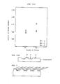
- Figure 2(a) shows a graph illustrating the relationship between the glass substrates and the amount of noise arising when information is read out from the optical memory element using each of the said glass substrates.
- Figure 2(b) is a front view showing a part of the glass substrate, wherein B, C, and D are the positions to each of which a laser beam is applied.
- Figure 3 is a perspective view showing a part of the glass substrate of the optical memory element of this invention.
- Figures 1(a) to 1(e) show schematic diagrams illustrating a process for the production of the substrate of an optical memory element of this invention.
- Step(1): A glass substrate having the surface polished with high accuracy is washed as a glass substrate of the optical memory element, and then, as shown in Figure 1(a), a photo-resist material is coated on the glass substrate 1 by a spinner to form a photo-
resist film 2. The glass substrate 1 is composed of a glass containing SiO₂ in the range of 51 to 71% by weight, Na₂0 in the range of 10 to 18% by weight, K₂0 in the range of 0 to 8% by weight, Al₂O₃ in the range of 12 to 22% by weight, and B₂O₃ in the range of 0 to 9% by weight. - Step(2): As shown in Figure 1(b), a masking board 3, on which guide groove information is patterned, is disposed on the glass substrate 1 covered by the photo-
resist film 2, and the UV rays A are applied to the masking board 3 to form the guide groove pattern latent image on the photo-resist film 2. - Step(3): The photo-
resist film 2, which has a guide groove pattern latent image thereon corresponding to the guide groove pattern of the masking board 3, is subjected to a developing treatment to form the guide grooves in the photo-resist film 2 as shown in Figure 1(c). - Step(4): The glass substrate 1 coated with the photo-
resist film 2 having the guide grooves is subjected to a dry etching treatment such as a sputtering treatment (a reactive etching treatment) or the like within an etching gas such as CF₄, CHF₃ or the like, resulting instriped grooves 4 in the glass substrate 1 as shown in Figure 1(d). - Step(5): The photo-
resist film 2 is removed from the glass substrate 1 by use of a solvent such as acetone, etc., or by means of the sputtering method, etc., in an O₂ atmosphere. Thus, thestriped grooves 4 which function as guide grooves or the like of a laser beam are formed in the glass substrate 1 as shown in Figure 1(e). - Figure 2(a) shows the relationship between the glass substrates and the amount of noise, wherein "GI" is the characteristics of the novel glass, which is used for the substrate of this invention, with a composition containing SiO₂ of 61% by weight, Na₂O of 13% by weight, K₂O of 3% by weight, Al₂O₃ of 17% by weight, B₂O₃ of 4% by weight, and the others of 2% by weight, and "G2" is the characteristics of a glass (i.e., a soda-lime glass), which is used for a conventional substrate, with a composition containing SiO₂ of 72% by weight, Na₂O of 15% by weight, Al₂O₃ of 2% by weight, CaO of 7% by weight, and MgO of 4% by weight.
- The amount of noise shown in Figure 2(a) is determined as follows: As shown in Figure 2(b), noise arising at the position D of the glass substrate, at which no groove is formed, is regenerated by an optical head, and the frequency of the noise is analyzed by a spectrum analyzer to obtain the amount of noise, S₀. In the same manner as the mentioned above, the amount of noise, S₁, at the position B of the glass substrate located between the grooves and the amount of noise, S₂, at the position C located in the groove of the glass substrate are obtained. Then, the difference N₁ in the amount of noise between the positions B and D and the difference N₂ in the amount of noise between the positions C and D are calculated using the values S₀, S₁ and S₂. The values S₀, N₁ and N₂ are plotted as shown in Figure 2(a), which indicates that the amount of noise at the position C in the groove of the conventional glass substrate made of the ordinary G2 type glass is greater by -70 dBm than that at the position D of the same glass substrate made of the ordinary G2 type glass, whereas the amount of noise at the position C in the groove of the glass substrate made of the novel G1 type glass of this invention is greater by -80 dBm than that at the position D of the same glass substrate made of the novel G1 type glass of this invention. The amount of noise at each of the positions D and B of the glass substrate made of the novel G1 type glass of this invention is nearly equal to that at each of the positions D and B of the conventional glass substrate made of the ordinary G2 type glass, and accordingly it can be seen that the polished state of the G1 type glass of this invention prior to the etching treatment is the same as that of the conventional G2 type glass prior to the etching treatment.
- The difference in the amount of noise between the G1 type glass and the G2 type glass caused by the formation of grooves in the glass substrates by an etching technique, is due to the difference in the composition between the G1 type glass and the G2 type glass. That is, the glass substrate made of the G1 type glass of this invention contains a relatively large amount of Al₂O₃ so that even though it is subjected to an etching treatment, the surface smoothness of the glass substrate can be maintained at the same level as before etching. On the contrary, the conventional glass substrate made of the G2 type glass, which is used for a conventional optical memory element, contains a small amount of Al₂O₃, so that once it is subjected to an etching treatment, the surface smoothness of the glass substrate is significantly damaged, which causes an increase in noise.
- Although the above-mentioned example disclosed the formation of grooves by a dry etching technique such as a reactive ion etching technique, a wet etching technique can be, of course, applied to the glass of this invention to thereby produce a high quality glass substrate which is useful for an optical memory element.
Claims (3)
Applications Claiming Priority (2)
| Application Number | Priority Date | Filing Date | Title |
|---|---|---|---|
| JP60270361A JPS62128944A (en) | 1985-11-27 | 1985-11-27 | Optical memory element |
| JP270361/85 | 1985-11-27 |
Publications (2)
| Publication Number | Publication Date |
|---|---|
| EP0228814A1 true EP0228814A1 (en) | 1987-07-15 |
| EP0228814B1 EP0228814B1 (en) | 1991-02-27 |
Family
ID=17485196
Family Applications (1)
| Application Number | Title | Priority Date | Filing Date |
|---|---|---|---|
| EP86309225A Expired - Lifetime EP0228814B1 (en) | 1985-11-27 | 1986-11-26 | An optical memory element |
Country Status (4)
| Country | Link |
|---|---|
| US (1) | US4818648A (en) |
| EP (1) | EP0228814B1 (en) |
| JP (1) | JPS62128944A (en) |
| DE (1) | DE3677741D1 (en) |
Cited By (7)
| Publication number | Priority date | Publication date | Assignee | Title |
|---|---|---|---|---|
| US4797316A (en) * | 1986-12-23 | 1989-01-10 | Glaverbel | Etched glass and process of manufacturing same |
| EP0310397A2 (en) * | 1987-09-29 | 1989-04-05 | Victor Company Of Japan, Limited | Information recording medium having a glass substrate |
| EP0527602A2 (en) * | 1991-08-09 | 1993-02-17 | Sharp Kabushiki Kaisha | Optical memory |
| US5499731A (en) * | 1994-01-07 | 1996-03-19 | Pilkington Plc | Substrate for a magnetic disc and manufacture thereof |
| FR2725713A1 (en) * | 1994-10-13 | 1996-04-19 | Saint Gobain Vitrage | Glass substrate |
| WO1996011888A1 (en) * | 1994-10-13 | 1996-04-25 | Saint-Gobain Vitrage S.A. | Reinforced glass substrates |
| US5895582A (en) * | 1992-07-09 | 1999-04-20 | Pilkington Plc | Process of manufacturing a glass substrate for a magnetic disk |
Families Citing this family (6)
| Publication number | Priority date | Publication date | Assignee | Title |
|---|---|---|---|---|
| US5170390A (en) * | 1988-08-22 | 1992-12-08 | Sharp Kabushiki Kaisha | Optical recording element and driving system |
| JP2982328B2 (en) * | 1991-01-23 | 1999-11-22 | ソニー株式会社 | Manufacturing method of high density optical disk |
| JPH04286736A (en) * | 1991-03-15 | 1992-10-12 | Sharp Corp | Production of substrate for master disk of optical memory element |
| US5674790A (en) * | 1995-12-15 | 1997-10-07 | Corning Incorporated | Strengthening glass by ion exchange |
| JP2002265233A (en) * | 2001-03-05 | 2002-09-18 | Nippon Sheet Glass Co Ltd | Glass preform for laser beam machining and glass for laser beam machining |
| RU2713044C1 (en) * | 2019-05-21 | 2020-02-03 | Российская Федерация, от имени которой выступает ФОНД ПЕРСПЕКТИВНЫХ ИССЛЕДОВАНИЙ | Optical information carrier based on oxide glasses |
Citations (4)
| Publication number | Priority date | Publication date | Assignee | Title |
|---|---|---|---|---|
| DE1287764B (en) * | 1964-09-16 | 1969-01-23 | ||
| DE1596782B1 (en) * | 1967-03-25 | 1970-12-10 | Deutsche Spiegelglas Ag | Mechanically and thermally shock-resistant glass |
| SU1089066A1 (en) * | 1982-05-05 | 1984-04-30 | Московский ордена Ленина и ордена Трудового Красного Знамени химико-технологический институт им.Д.И.Менделеева | Glass |
| US4544443A (en) * | 1983-05-13 | 1985-10-01 | Shap Kabushiki Kaisha | Method for manufacturing an optical memory element |
Family Cites Families (4)
| Publication number | Priority date | Publication date | Assignee | Title |
|---|---|---|---|---|
| US4015045A (en) * | 1974-01-09 | 1977-03-29 | Ppg Industries, Inc. | Chemical strengthening of glass |
| JPS59227049A (en) * | 1983-06-07 | 1984-12-20 | Fuji Photo Film Co Ltd | Information recording medium |
| JPS60122748A (en) * | 1983-12-06 | 1985-07-01 | Nippon Sheet Glass Co Ltd | Aluminosilicate glass |
| JPH0648546B2 (en) * | 1984-07-14 | 1994-06-22 | 日本ビクター株式会社 | Method of manufacturing information record carrier |
-
1985
- 1985-11-27 JP JP60270361A patent/JPS62128944A/en active Granted
-
1986
- 1986-11-25 US US06/934,718 patent/US4818648A/en not_active Expired - Lifetime
- 1986-11-26 EP EP86309225A patent/EP0228814B1/en not_active Expired - Lifetime
- 1986-11-26 DE DE8686309225T patent/DE3677741D1/en not_active Expired - Lifetime
Patent Citations (4)
| Publication number | Priority date | Publication date | Assignee | Title |
|---|---|---|---|---|
| DE1287764B (en) * | 1964-09-16 | 1969-01-23 | ||
| DE1596782B1 (en) * | 1967-03-25 | 1970-12-10 | Deutsche Spiegelglas Ag | Mechanically and thermally shock-resistant glass |
| SU1089066A1 (en) * | 1982-05-05 | 1984-04-30 | Московский ордена Ленина и ордена Трудового Красного Знамени химико-технологический институт им.Д.И.Менделеева | Glass |
| US4544443A (en) * | 1983-05-13 | 1985-10-01 | Shap Kabushiki Kaisha | Method for manufacturing an optical memory element |
Non-Patent Citations (1)
| Title |
|---|
| SOVIET INVENTIONS ILLUSTRATED Section CH Week 198449, 23 January 1985 Derwent World Patents Index; * |
Cited By (13)
| Publication number | Priority date | Publication date | Assignee | Title |
|---|---|---|---|---|
| US4797316A (en) * | 1986-12-23 | 1989-01-10 | Glaverbel | Etched glass and process of manufacturing same |
| EP0310397A2 (en) * | 1987-09-29 | 1989-04-05 | Victor Company Of Japan, Limited | Information recording medium having a glass substrate |
| EP0310397A3 (en) * | 1987-09-29 | 1990-06-27 | Victor Company Of Japan, Limited | Information recording medium having a glass substrate |
| US5008176A (en) * | 1987-09-29 | 1991-04-16 | Victor Company Of Japan, Ltd. | Information recording medium having a glass substrate |
| US5586109A (en) * | 1991-08-09 | 1996-12-17 | Sharp Kabushiki Kaisha | Optical memory having narrowed track pitch |
| EP0527602A3 (en) * | 1991-08-09 | 1993-03-31 | Sharp Kabushiki Kaisha | Optical memory |
| EP0527602A2 (en) * | 1991-08-09 | 1993-02-17 | Sharp Kabushiki Kaisha | Optical memory |
| US5676854A (en) * | 1991-08-09 | 1997-10-14 | Sharp Kabushiki Kaisha | Optical memory having narrowed track pitch |
| US5895582A (en) * | 1992-07-09 | 1999-04-20 | Pilkington Plc | Process of manufacturing a glass substrate for a magnetic disk |
| US5499731A (en) * | 1994-01-07 | 1996-03-19 | Pilkington Plc | Substrate for a magnetic disc and manufacture thereof |
| US5681636A (en) * | 1994-01-07 | 1997-10-28 | Pilkington Plc | Magnetic recording disc substrate having a surface texture of non overlapping circular sub-arrays |
| FR2725713A1 (en) * | 1994-10-13 | 1996-04-19 | Saint Gobain Vitrage | Glass substrate |
| WO1996011888A1 (en) * | 1994-10-13 | 1996-04-25 | Saint-Gobain Vitrage S.A. | Reinforced glass substrates |
Also Published As
| Publication number | Publication date |
|---|---|
| JPH04935B2 (en) | 1992-01-09 |
| US4818648A (en) | 1989-04-04 |
| JPS62128944A (en) | 1987-06-11 |
| DE3677741D1 (en) | 1991-04-04 |
| EP0228814B1 (en) | 1991-02-27 |
Similar Documents
| Publication | Publication Date | Title |
|---|---|---|
| EP0446967B1 (en) | An optical memory element | |
| EP0228814B1 (en) | An optical memory element | |
| EP0155000B1 (en) | Method of manufacturing optical memory element | |
| EP0310397B1 (en) | Information recording medium having a glass substrate | |
| US4288510A (en) | Process of making an optically recordable and readable information carrier and the carrier obtained by this process | |
| EP0136041A1 (en) | Optical memory disc | |
| EP0178116B1 (en) | Optical memory element | |
| EP0145344A1 (en) | Optical memory disc | |
| US4839251A (en) | Photo-mask for use in manufacturing an optical memory disc, a method for making the photo-mask and a method for manufacturing the optical memory disc | |
| EP0239188B1 (en) | Preformatted optical recording medium and method of producing the same | |
| EP0319350A2 (en) | Method of and photomask for manufacturing optical memory element | |
| US5166014A (en) | Method for the manufacture of an optically readable disc, and discs obtained by this method | |
| US5336531A (en) | Magneto-optical disk and manufacturing methods thereof | |
| CA2056308C (en) | Method for manufacturing a photomask for an optical memory | |
| JPH0373938B2 (en) | ||
| JP2708847B2 (en) | Optical disk stamper and method of manufacturing the same | |
| JPS59210547A (en) | Manufacture of optical memory element | |
| JPH0762249B2 (en) | Optical disk manufacturing equipment | |
| KR100230239B1 (en) | Mastering device for manufacturing optical disc | |
| JP2532274B2 (en) | optical disk | |
| MY105701A (en) | Interactive optical disk. | |
| JPH0770089B2 (en) | Optical information carrier disk | |
| JPS6275952A (en) | Production of optical memory element | |
| WO1999004395A1 (en) | Creation of graphic images on a data disc | |
| JPH0585972B2 (en) |
Legal Events
| Date | Code | Title | Description |
|---|---|---|---|
| PUAI | Public reference made under article 153(3) epc to a published international application that has entered the european phase |
Free format text: ORIGINAL CODE: 0009012 |
|
| 17P | Request for examination filed |
Effective date: 19861215 |
|
| AK | Designated contracting states |
Kind code of ref document: A1 Designated state(s): DE FR GB |
|
| 17Q | First examination report despatched |
Effective date: 19890623 |
|
| GRAA | (expected) grant |
Free format text: ORIGINAL CODE: 0009210 |
|
| AK | Designated contracting states |
Kind code of ref document: B1 Designated state(s): DE FR GB |
|
| REF | Corresponds to: |
Ref document number: 3677741 Country of ref document: DE Date of ref document: 19910404 |
|
| ET | Fr: translation filed | ||
| PLBE | No opposition filed within time limit |
Free format text: ORIGINAL CODE: 0009261 |
|
| STAA | Information on the status of an ep patent application or granted ep patent |
Free format text: STATUS: NO OPPOSITION FILED WITHIN TIME LIMIT |
|
| 26N | No opposition filed | ||
| REG | Reference to a national code |
Ref country code: GB Ref legal event code: IF02 |
|
| PGFP | Annual fee paid to national office [announced via postgrant information from national office to epo] |
Ref country code: FR Payment date: 20041109 Year of fee payment: 19 |
|
| PGFP | Annual fee paid to national office [announced via postgrant information from national office to epo] |
Ref country code: DE Payment date: 20041118 Year of fee payment: 19 |
|
| PGFP | Annual fee paid to national office [announced via postgrant information from national office to epo] |
Ref country code: GB Payment date: 20041124 Year of fee payment: 19 |
|
| PG25 | Lapsed in a contracting state [announced via postgrant information from national office to epo] |
Ref country code: GB Free format text: LAPSE BECAUSE OF NON-PAYMENT OF DUE FEES Effective date: 20051126 |
|
| PG25 | Lapsed in a contracting state [announced via postgrant information from national office to epo] |
Ref country code: DE Free format text: LAPSE BECAUSE OF NON-PAYMENT OF DUE FEES Effective date: 20060601 |
|
| GBPC | Gb: european patent ceased through non-payment of renewal fee |
Effective date: 20051126 |
|
| PG25 | Lapsed in a contracting state [announced via postgrant information from national office to epo] |
Ref country code: FR Free format text: LAPSE BECAUSE OF NON-PAYMENT OF DUE FEES Effective date: 20060731 |
|
| REG | Reference to a national code |
Ref country code: FR Ref legal event code: ST Effective date: 20060731 |