EP0228278A2 - Assemblage connecteur électrique - Google Patents
Assemblage connecteur électrique Download PDFInfo
- Publication number
- EP0228278A2 EP0228278A2 EP86310062A EP86310062A EP0228278A2 EP 0228278 A2 EP0228278 A2 EP 0228278A2 EP 86310062 A EP86310062 A EP 86310062A EP 86310062 A EP86310062 A EP 86310062A EP 0228278 A2 EP0228278 A2 EP 0228278A2
- Authority
- EP
- European Patent Office
- Prior art keywords
- component
- casing
- terminals
- connector assembly
- printed circuit
- Prior art date
- Legal status (The legal status is an assumption and is not a legal conclusion. Google has not performed a legal analysis and makes no representation as to the accuracy of the status listed.)
- Withdrawn
Links
Images

Classifications
-
- G—PHYSICS
- G06—COMPUTING; CALCULATING OR COUNTING
- G06K—GRAPHICAL DATA READING; PRESENTATION OF DATA; RECORD CARRIERS; HANDLING RECORD CARRIERS
- G06K7/00—Methods or arrangements for sensing record carriers, e.g. for reading patterns
- G06K7/0013—Methods or arrangements for sensing record carriers, e.g. for reading patterns by galvanic contacts, e.g. card connectors for ISO-7816 compliant smart cards or memory cards, e.g. SD card readers
- G06K7/0056—Methods or arrangements for sensing record carriers, e.g. for reading patterns by galvanic contacts, e.g. card connectors for ISO-7816 compliant smart cards or memory cards, e.g. SD card readers housing of the card connector
- G06K7/0082—Methods or arrangements for sensing record carriers, e.g. for reading patterns by galvanic contacts, e.g. card connectors for ISO-7816 compliant smart cards or memory cards, e.g. SD card readers housing of the card connector comprising an arrangement for protection against electrostatic discharge, e.g. by grounding part of the conductive housing
-
- G—PHYSICS
- G06—COMPUTING; CALCULATING OR COUNTING
- G06K—GRAPHICAL DATA READING; PRESENTATION OF DATA; RECORD CARRIERS; HANDLING RECORD CARRIERS
- G06K7/00—Methods or arrangements for sensing record carriers, e.g. for reading patterns
- G06K7/0013—Methods or arrangements for sensing record carriers, e.g. for reading patterns by galvanic contacts, e.g. card connectors for ISO-7816 compliant smart cards or memory cards, e.g. SD card readers
- G06K7/0047—Methods or arrangements for sensing record carriers, e.g. for reading patterns by galvanic contacts, e.g. card connectors for ISO-7816 compliant smart cards or memory cards, e.g. SD card readers for reading/sensing record carriers having edge contacts
-
- H—ELECTRICITY
- H01—ELECTRIC ELEMENTS
- H01R—ELECTRICALLY-CONDUCTIVE CONNECTIONS; STRUCTURAL ASSOCIATIONS OF A PLURALITY OF MUTUALLY-INSULATED ELECTRICAL CONNECTING ELEMENTS; COUPLING DEVICES; CURRENT COLLECTORS
- H01R13/00—Details of coupling devices of the kinds covered by groups H01R12/70 or H01R24/00 - H01R33/00
- H01R13/648—Protective earth or shield arrangements on coupling devices, e.g. anti-static shielding
- H01R13/6485—Electrostatic discharge protection
-
- H—ELECTRICITY
- H01—ELECTRIC ELEMENTS
- H01R—ELECTRICALLY-CONDUCTIVE CONNECTIONS; STRUCTURAL ASSOCIATIONS OF A PLURALITY OF MUTUALLY-INSULATED ELECTRICAL CONNECTING ELEMENTS; COUPLING DEVICES; CURRENT COLLECTORS
- H01R13/00—Details of coupling devices of the kinds covered by groups H01R12/70 or H01R24/00 - H01R33/00
- H01R13/648—Protective earth or shield arrangements on coupling devices, e.g. anti-static shielding
Definitions
- This invention relates to an electrical connector assembly of the type which has one connector component mounted to a printed circuit board and another connector component which incorporates a semiconductor circuit or IC package which is inserted into the first component. In this way the semiconductor circuit or IC package can be electrically connected to a circuit on the printed circuit board or disengaged.
- the first component mounted to the printed circuit board has a casing with an opening for receiving the other component carrying or otherwise incorporating the IC package.
- Complementary terminals in the casings of the components make connection whereby to connect the IC package to a circuit on the printed circuit boad.
- a connection assembly comprises: a first component having a casing with an opening; a second component adapted to be inserted into the opening of the casing of the first component and incorporating a semiconductor circuit as an IC package and respective terminals of the components disposed at least partially within the casings thereof for establishing connection between the IC package and means exterior to the first component.
- at least one grounding terminal is mounted to the casing of the first component to contact the casing of the second component when the components are brought together to provide a grounding path for electrostatic charge.
- the casing of the first component would normally be mounted to a printed circuit board and a screw can penetrate the grounding terminal to clamp the casing to the printed circuit board and provide a good grounding connection thereto.
- the grounding terminal is preferably a conductive resilient metal strip which contacts the casing of the second component before the terminals interconnect thereby to discharge any static electricity developed on the casing prior to connection of the IC package.
- Figs. 1 and 2 show a conventional connector assembly suitable for interconnecting a semiconductor circuit, such as a memory, CPU and the like in the form of a card-like, flat IC package to another circuit usually on a printed circuit board.
- the connector assembly comprises a component 30 incorporating an IC package not shown but notionally referenced 32 and a component 40 mounted to a printed circuit board (not shown).
- the connector component 30 has a sheet-like housing 31 with a recessed portion 33 containing connection terminals 34.
- Each terminal 34 is attached to the inner surface of the housing 31 and inner ends 34a of the terminals 34 extend into the housing 31 for connection to the semiconductor circuit 32.
- the terminals 34 have socket portions 34b formed at their other ends which open from the recessed portion 33 for access.
- the component 40 is composed of a casing 42 having an opening 41 into which the component 30 with the IC package 32 is inserted.
- Connection terminals 43 are arranged at an end portion of the casing 42 remote from the opening 41.
- the terminals 43 have pins 43b for connection with the printed circuit board.
- One end 43a of each connection terminal 43 extends into the interior of the casing 42, and is also shaped as a pin for insertion into the socket portion 34b of a corresponding one of the connection terminals 34 of the component as shown in Fig. 2.
- the component 30 with the IC package 32 can be inserted into the opening 41 to establish connection between the IC package 32 and the printed circuit board via the connection terminals 34 and 43. If the connector component 30 carries an electrostatic charge, the semiconductor can be destroyed.
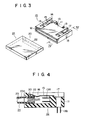
- FIG. 3 and 4 of the accompanying drawings which are generally similar to Figs. 1 and 2.
- the connector assembly again is composed of a connector component 10 which is attached to a printed circuit board, and a connector component 20 incorporating an IC package.
- the connector component 20 has a casing 21 with a recessed portion 22 containing terminals 23 with socket portions 23b connected to the IC package via portions 23a.
- the connector component 10 has a casing 11 with an opening 12 for receiving the casing 21.
- Terminals 13 mounted on the casing 11 to the rear of the opening 12 have pins 13a projecting within the opening 12 which are engageable with the socket portions 23b and further depending pins 13b for connection with the tracks on the printed circuit board.
- each terminal 15 is made from a conductive, resilient metal.
- the slots 14 penetrate into the opening 12 and the grounding terminals 15 have shaped end regions 16 disposed further from the rear end of the casing 11 than the pins 13a.
- Holes 17 are formed in the rear end portions of the grounding terminals 15 remote from extension 16 which align with bores in the casing 21. Screws can be located through the holes and bores to fix the component 10 to the printed circuit board and establish a good grounding path.
- Figs. 1 and 2 if the IC package and the connector casing 21 are in an electrically charged state, discharge is reliably effected through the grounding terminals 15. Therefore, no static electricity problems occur upon making contact between the connection terminals 23 and 13.
- the casing 21, when fully inserted into the casing 11 is resiliently retained by the bent or curved portions 16 of the grounding terminals 15. The constant contact between the terminals 15 and the casing 21 also precludes any further build-up of static electricity. As a result, there is no risk that the semiconductor circuit can be destroyed by electrostatic discharge.
- the grounding terminals 15 are simple in structure and easy to attach to the casing 11. Also, since the grounding terminals 15 are mounted in proximity to the side edges of the casing 11, that is, at the zones where the connection terminals 13 are not located no further modification of the casing 11 is needed.
- grounding terminals 15 are preferred in the embodiment just described it is possible to use a single grounding terminal.
Applications Claiming Priority (2)
| Application Number | Priority Date | Filing Date | Title |
|---|---|---|---|
| JP201864/85U | 1985-12-27 | ||
| JP1985201864U JPS62111187U (fr) | 1985-12-27 | 1985-12-27 |
Publications (2)
| Publication Number | Publication Date |
|---|---|
| EP0228278A2 true EP0228278A2 (fr) | 1987-07-08 |
| EP0228278A3 EP0228278A3 (fr) | 1988-11-17 |
Family
ID=16448154
Family Applications (1)
| Application Number | Title | Priority Date | Filing Date |
|---|---|---|---|
| EP86310062A Withdrawn EP0228278A3 (fr) | 1985-12-27 | 1986-12-23 | Assemblage connecteur électrique |
Country Status (5)
| Country | Link |
|---|---|
| EP (1) | EP0228278A3 (fr) |
| JP (1) | JPS62111187U (fr) |
| AU (1) | AU6697586A (fr) |
| BR (1) | BR8606374A (fr) |
| MX (1) | MX160627A (fr) |
Cited By (30)
| Publication number | Priority date | Publication date | Assignee | Title |
|---|---|---|---|---|
| EP0406610A2 (fr) * | 1989-07-05 | 1991-01-09 | Seiko Epson Corporation | Structure éliminant l'électricité statique pour des dispositifs électroniques |
| EP0468748A1 (fr) * | 1990-07-24 | 1992-01-29 | Yamaichi Electronics Co., Ltd. | Socle pour dispositif électrique |
| US5357402A (en) * | 1992-02-24 | 1994-10-18 | Itt Corporation | Card-receiving electronic device having grounding spring |
| EP0635801A2 (fr) * | 1993-07-23 | 1995-01-25 | Kabushiki Kaisha Toshiba | Dispositif de mémoire externe |
| EP0661912A2 (fr) * | 1993-12-30 | 1995-07-05 | Robert Bosch Gmbh | Appareil électrique alimenté par batterie |
| WO1995030259A1 (fr) * | 1994-04-29 | 1995-11-09 | The Whitaker Corporation | Enveloppe conductrice pour connecteurs electriques |
| WO1996004698A1 (fr) * | 1994-07-29 | 1996-02-15 | The Whitaker Corporation | Enveloppe de protection de mise a la terre amelioree pour connecteurs electriques |
| EP0756241A2 (fr) * | 1995-06-14 | 1997-01-29 | AMPHENOL-TUCHEL ELECTRONICS GmbH | Dispositif de contact blindé |
| US5717533A (en) * | 1995-01-13 | 1998-02-10 | Methode Electronics Inc. | Removable optoelectronic module |
| US5822190A (en) * | 1996-06-11 | 1998-10-13 | Kabushiki Kaisha Toshiba | Card type memory device and a method for manufacturing the same |
| US5879173A (en) * | 1995-01-13 | 1999-03-09 | Methode Electronics, Inc. | Removable transceiver module and receptacle |
| EP0919933A2 (fr) * | 1997-11-27 | 1999-06-02 | Murata Manufacturing Co., Ltd. | Carte PC compatible en commutation avec des modes 16 bits et 32 bits |
| US6002605A (en) * | 1997-02-28 | 1999-12-14 | Kabushiki Kaisha Toshiba | Connecting apparatus, and information processing apparatus |
| US6022763A (en) * | 1996-05-10 | 2000-02-08 | Kabushiki Kaisha Toshiba | Substrate for semiconductor device, semiconductor device using the same, and method for manufacture thereof |
| US6054774A (en) * | 1994-03-22 | 2000-04-25 | Kabushiki Kaisha Toshiba | Thin type semiconductor package |
| USRE36820E (en) | 1995-01-13 | 2000-08-15 | Methode Electronics, Inc. | Removable optoelectronic module |
| US6166431A (en) * | 1995-08-25 | 2000-12-26 | Kabushiki Kaisha Tishiba | Semiconductor device with a thickness of 1 MM or less |
| EP0774727A3 (fr) * | 1995-11-17 | 2001-01-03 | Kabushiki Kaisha Toshiba | Lecteur/enregistreur de carte à puce |
| US6179627B1 (en) | 1998-04-22 | 2001-01-30 | Stratos Lightwave, Inc. | High speed interface converter module |
| US6201295B1 (en) | 1993-04-28 | 2001-03-13 | Kabushiki Kaisha Toshiba | Plate-shaped external storage device and method of producing the same |
| US6203333B1 (en) | 1998-04-22 | 2001-03-20 | Stratos Lightwave, Inc. | High speed interface converter module |
| US6220878B1 (en) | 1995-10-04 | 2001-04-24 | Methode Electronics, Inc. | Optoelectronic module with grounding means |
| US6220873B1 (en) | 1999-08-10 | 2001-04-24 | Stratos Lightwave, Inc. | Modified contact traces for interface converter |
| US6252791B1 (en) | 1991-04-11 | 2001-06-26 | Sandisk Corporation | Computer memory cards using flash EEPROM integrated circuit chips and memory-controller systems |
| US6266724B1 (en) | 1993-09-01 | 2001-07-24 | Sandisk Corporation | Removable mother/daughter peripheral card |
| WO2002065378A1 (fr) * | 2001-02-14 | 2002-08-22 | Smartdata S.A. | Dispositif modulaire de cartes a puces |
| US6893268B1 (en) | 1993-09-01 | 2005-05-17 | Sandisk Corporation | Removable mother/daughter peripheral card |
| US6966785B2 (en) * | 2002-10-23 | 2005-11-22 | J.S.T. Mfg. Co., Ltd. | Connector |
| US7114047B2 (en) * | 1998-12-10 | 2006-09-26 | Kabushiki Kaisha Toshiba | Data storage medium with certification data |
| DE19655315B4 (de) * | 1995-01-13 | 2014-10-02 | Methode Electronics, Inc. | Entfernbares Sender/Empfänger-Modul und -Aufnahme |
Families Citing this family (3)
| Publication number | Priority date | Publication date | Assignee | Title |
|---|---|---|---|---|
| JP4527887B2 (ja) * | 2001-01-24 | 2010-08-18 | 京セラエルコ株式会社 | カードコネクタの誤挿入防止装置 |
| JP5281190B1 (ja) * | 2012-12-12 | 2013-09-04 | 利仁 曽根 | Usbコネクタを含む電気コネクタ・システム |
| JP6583474B2 (ja) * | 2018-04-27 | 2019-10-02 | 山一電機株式会社 | プラグ、ソケット、および、それらを備える基板接続用コネクタ |
Citations (3)
| Publication number | Priority date | Publication date | Assignee | Title |
|---|---|---|---|---|
| US4012672A (en) * | 1975-03-28 | 1977-03-15 | Motorola, Inc. | Plug-in module for electronic device having component forming a guide for aligning the module |
| EP0040941A1 (fr) * | 1980-05-28 | 1981-12-02 | AMP INCORPORATED (a New Jersey corporation) | Blindage pour un connecteur électrique |
| US4389080A (en) * | 1981-07-15 | 1983-06-21 | General Electric | Plug-in ceramic hybrid module |
Family Cites Families (1)
| Publication number | Priority date | Publication date | Assignee | Title |
|---|---|---|---|---|
| US4386814A (en) * | 1981-08-17 | 1983-06-07 | Amp Incorporated | Kit for converting a panel opening to a shielded pin receptacle |
-
1985
- 1985-12-27 JP JP1985201864U patent/JPS62111187U/ja active Pending
-
1986
- 1986-12-22 BR BR8606374A patent/BR8606374A/pt unknown
- 1986-12-23 EP EP86310062A patent/EP0228278A3/fr not_active Withdrawn
- 1986-12-24 AU AU66975/86A patent/AU6697586A/en not_active Abandoned
- 1986-12-24 MX MX864796A patent/MX160627A/es unknown
Patent Citations (3)
| Publication number | Priority date | Publication date | Assignee | Title |
|---|---|---|---|---|
| US4012672A (en) * | 1975-03-28 | 1977-03-15 | Motorola, Inc. | Plug-in module for electronic device having component forming a guide for aligning the module |
| EP0040941A1 (fr) * | 1980-05-28 | 1981-12-02 | AMP INCORPORATED (a New Jersey corporation) | Blindage pour un connecteur électrique |
| US4389080A (en) * | 1981-07-15 | 1983-06-21 | General Electric | Plug-in ceramic hybrid module |
Cited By (57)
| Publication number | Priority date | Publication date | Assignee | Title |
|---|---|---|---|---|
| EP0406610A3 (en) * | 1989-07-05 | 1991-06-05 | Seiko Epson Corporation | Static electricity eliminating structure for electronic devices |
| EP0406610A2 (fr) * | 1989-07-05 | 1991-01-09 | Seiko Epson Corporation | Structure éliminant l'électricité statique pour des dispositifs électroniques |
| EP0468748A1 (fr) * | 1990-07-24 | 1992-01-29 | Yamaichi Electronics Co., Ltd. | Socle pour dispositif électrique |
| US7106609B2 (en) | 1991-04-11 | 2006-09-12 | Sandisk Corporation | Computer memory cards using flash EEPROM integrated circuit chips and memory-controller systems |
| US7355874B2 (en) | 1991-04-11 | 2008-04-08 | Sandisk Corporation | Computer memory cards using flash EEprom integrated circuit chips and memory-controller systems |
| US6628537B1 (en) | 1991-04-11 | 2003-09-30 | Sandisk Corporation | Computer memory cards using flash EEPROM integrated circuit chips and memory-controller systems |
| US6947332B2 (en) | 1991-04-11 | 2005-09-20 | Sandisk Corporation | Computer memory cards using flash EEPROM integrated circuit chips and memory-controller systems |
| US6434034B1 (en) | 1991-04-11 | 2002-08-13 | Sandisk Corporation | Computer memory cards using flash EEPROM integrated circuit chips and memory-controller systems |
| US6252791B1 (en) | 1991-04-11 | 2001-06-26 | Sandisk Corporation | Computer memory cards using flash EEPROM integrated circuit chips and memory-controller systems |
| US5357402A (en) * | 1992-02-24 | 1994-10-18 | Itt Corporation | Card-receiving electronic device having grounding spring |
| US6201295B1 (en) | 1993-04-28 | 2001-03-13 | Kabushiki Kaisha Toshiba | Plate-shaped external storage device and method of producing the same |
| US6274926B1 (en) | 1993-04-28 | 2001-08-14 | Kabushiki Kaisha Toshiba | Plate-shaped external storage device and method of producing the same |
| EP0635801A2 (fr) * | 1993-07-23 | 1995-01-25 | Kabushiki Kaisha Toshiba | Dispositif de mémoire externe |
| EP0635801A3 (fr) * | 1993-07-23 | 1996-06-12 | Toshiba Kk | Dispositif de mémoire externe. |
| US6147861A (en) * | 1993-07-23 | 2000-11-14 | Kabushiki Kaisha Toshiba | External storage device unit |
| US6362957B1 (en) | 1993-07-23 | 2002-03-26 | Kabushiki Kaisha Toshiba | External storage device |
| US6147860A (en) * | 1993-07-23 | 2000-11-14 | Kabushiki Kaisha Toshiba | External storage device |
| US6141210A (en) * | 1993-07-23 | 2000-10-31 | Kabushiki Kaisha Toshiba | External storage device |
| EP1024453A1 (fr) * | 1993-07-23 | 2000-08-02 | Kabushiki Kaisha Toshiba | Dispositif de mémoire externe |
| US6981068B1 (en) | 1993-09-01 | 2005-12-27 | Sandisk Corporation | Removable mother/daughter peripheral card |
| US6381662B1 (en) | 1993-09-01 | 2002-04-30 | Sandisk Corporation | Removable mother/daughter peripheral card |
| US6266724B1 (en) | 1993-09-01 | 2001-07-24 | Sandisk Corporation | Removable mother/daughter peripheral card |
| US7137011B1 (en) | 1993-09-01 | 2006-11-14 | Sandisk Corporation | Removable mother/daughter peripheral card |
| US6893268B1 (en) | 1993-09-01 | 2005-05-17 | Sandisk Corporation | Removable mother/daughter peripheral card |
| EP0661912A2 (fr) * | 1993-12-30 | 1995-07-05 | Robert Bosch Gmbh | Appareil électrique alimenté par batterie |
| EP0661912A3 (fr) * | 1993-12-30 | 1995-11-08 | Bosch Gmbh Robert | Appareil électrique alimenté par batterie. |
| US6054774A (en) * | 1994-03-22 | 2000-04-25 | Kabushiki Kaisha Toshiba | Thin type semiconductor package |
| WO1995030259A1 (fr) * | 1994-04-29 | 1995-11-09 | The Whitaker Corporation | Enveloppe conductrice pour connecteurs electriques |
| CN1094668C (zh) * | 1994-04-29 | 2002-11-20 | 惠特克公司 | 用于电气连接件的导电罩壳 |
| CN1099728C (zh) * | 1994-07-29 | 2003-01-22 | 惠特克公司 | 改进的电气连接器的接地屏蔽 |
| WO1996004698A1 (fr) * | 1994-07-29 | 1996-02-15 | The Whitaker Corporation | Enveloppe de protection de mise a la terre amelioree pour connecteurs electriques |
| US6201704B1 (en) | 1995-01-13 | 2001-03-13 | Stratos Lightwave, Inc. | Transceive module with EMI shielding |
| US5879173A (en) * | 1995-01-13 | 1999-03-09 | Methode Electronics, Inc. | Removable transceiver module and receptacle |
| US5717533A (en) * | 1995-01-13 | 1998-02-10 | Methode Electronics Inc. | Removable optoelectronic module |
| DE19655315B4 (de) * | 1995-01-13 | 2014-10-02 | Methode Electronics, Inc. | Entfernbares Sender/Empfänger-Modul und -Aufnahme |
| US6267606B1 (en) | 1995-01-13 | 2001-07-31 | Stratos Lightwave, Inc. | Removable transceiver module and receptacle |
| USRE36820E (en) | 1995-01-13 | 2000-08-15 | Methode Electronics, Inc. | Removable optoelectronic module |
| EP0756241A3 (fr) * | 1995-06-14 | 2000-11-08 | AMPHENOL-TUCHEL ELECTRONICS GmbH | Dispositif de contact blindé |
| EP0756241A2 (fr) * | 1995-06-14 | 1997-01-29 | AMPHENOL-TUCHEL ELECTRONICS GmbH | Dispositif de contact blindé |
| US6333212B1 (en) | 1995-08-25 | 2001-12-25 | Kabushiki Kaisha Toshiba | Semiconductor device and manufacturing method thereof |
| US6166431A (en) * | 1995-08-25 | 2000-12-26 | Kabushiki Kaisha Tishiba | Semiconductor device with a thickness of 1 MM or less |
| US6220878B1 (en) | 1995-10-04 | 2001-04-24 | Methode Electronics, Inc. | Optoelectronic module with grounding means |
| EP0774727A3 (fr) * | 1995-11-17 | 2001-01-03 | Kabushiki Kaisha Toshiba | Lecteur/enregistreur de carte à puce |
| US6022763A (en) * | 1996-05-10 | 2000-02-08 | Kabushiki Kaisha Toshiba | Substrate for semiconductor device, semiconductor device using the same, and method for manufacture thereof |
| US5822190A (en) * | 1996-06-11 | 1998-10-13 | Kabushiki Kaisha Toshiba | Card type memory device and a method for manufacturing the same |
| US6085412A (en) * | 1996-06-11 | 2000-07-11 | Kabushiki Kaisha Toshiba | Method for manufacturing card type memory device |
| US6002605A (en) * | 1997-02-28 | 1999-12-14 | Kabushiki Kaisha Toshiba | Connecting apparatus, and information processing apparatus |
| US6137710A (en) * | 1997-02-28 | 2000-10-24 | Kabushiki Kaisha Toshiba | Connecting apparatus, and information processing apparatus |
| EP0919933A3 (fr) * | 1997-11-27 | 2002-08-28 | Murata Manufacturing Co., Ltd. | Carte PC compatible en commutation avec des modes 16 bits et 32 bits |
| EP0919933A2 (fr) * | 1997-11-27 | 1999-06-02 | Murata Manufacturing Co., Ltd. | Carte PC compatible en commutation avec des modes 16 bits et 32 bits |
| US6203333B1 (en) | 1998-04-22 | 2001-03-20 | Stratos Lightwave, Inc. | High speed interface converter module |
| US6179627B1 (en) | 1998-04-22 | 2001-01-30 | Stratos Lightwave, Inc. | High speed interface converter module |
| US7114047B2 (en) * | 1998-12-10 | 2006-09-26 | Kabushiki Kaisha Toshiba | Data storage medium with certification data |
| US6220873B1 (en) | 1999-08-10 | 2001-04-24 | Stratos Lightwave, Inc. | Modified contact traces for interface converter |
| EP1244048A1 (fr) * | 2001-02-14 | 2002-09-25 | Smartdata SA | Dispositif modulaire de cartes à puces |
| WO2002065378A1 (fr) * | 2001-02-14 | 2002-08-22 | Smartdata S.A. | Dispositif modulaire de cartes a puces |
| US6966785B2 (en) * | 2002-10-23 | 2005-11-22 | J.S.T. Mfg. Co., Ltd. | Connector |
Also Published As
| Publication number | Publication date |
|---|---|
| BR8606374A (pt) | 1987-10-13 |
| MX160627A (es) | 1990-03-29 |
| AU6697586A (en) | 1987-07-02 |
| JPS62111187U (fr) | 1987-07-15 |
| EP0228278A3 (fr) | 1988-11-17 |
Similar Documents
| Publication | Publication Date | Title |
|---|---|---|
| EP0228278A2 (fr) | Assemblage connecteur électrique | |
| US4867690A (en) | Electrical connector system | |
| US4975066A (en) | Coaxial contact element | |
| EP0772898B1 (fr) | Enveloppe de protection de mise a la terre amelioree pour connecteurs electriques | |
| US4264114A (en) | Electrical connector assembly | |
| EP0829930B1 (fr) | Connecteur électrique avec contacts de puissance | |
| US4400049A (en) | Connector for interconnecting circuit boards | |
| US5876241A (en) | Horizontal battery connector | |
| KR940002006B1 (ko) | 전기 코넥터의 신호보전용 기준도체 | |
| US5697799A (en) | Board-mountable shielded electrical connector | |
| US5046955A (en) | Active connector assembly | |
| JP3423560B2 (ja) | コネクタ | |
| US4558917A (en) | Electrical connector assembly | |
| EP0280449B1 (fr) | Connecteur de surface | |
| US5613860A (en) | Universal grounding clip for card-receiving connector | |
| US3413594A (en) | Edge connector | |
| JPS60109187A (ja) | 電気コネクタ | |
| EP0961365A3 (fr) | Connecteur électrique modulaire | |
| US5975958A (en) | Capactive coupling adapter for an electrical connector | |
| US5174764A (en) | Connector assembly having surface mounted terminals | |
| US5281155A (en) | Electrical connector with electrostatic discharge protection | |
| EP0397075A3 (fr) | Connecteur de bordure pour plaque à circuits imprimés | |
| US6132258A (en) | Board to board electrical connector | |
| US4892492A (en) | Device with openings for receiving pins of electrical components | |
| MY130144A (en) | Connector with press-fit terminal pins |
Legal Events
| Date | Code | Title | Description |
|---|---|---|---|
| PUAI | Public reference made under article 153(3) epc to a published international application that has entered the european phase |
Free format text: ORIGINAL CODE: 0009012 |
|
| AK | Designated contracting states |
Kind code of ref document: A2 Designated state(s): AT BE CH DE ES FR GB IT LI LU NL SE |
|
| PUAL | Search report despatched |
Free format text: ORIGINAL CODE: 0009013 |
|
| AK | Designated contracting states |
Kind code of ref document: A3 Designated state(s): AT BE CH DE ES FR GB IT LI LU NL SE |
|
| 17P | Request for examination filed |
Effective date: 19881104 |
|
| 17Q | First examination report despatched |
Effective date: 19901106 |
|
| STAA | Information on the status of an ep patent application or granted ep patent |
Free format text: STATUS: THE APPLICATION IS DEEMED TO BE WITHDRAWN |
|
| 18D | Application deemed to be withdrawn |
Effective date: 19910319 |
|
| RIN1 | Information on inventor provided before grant (corrected) |
Inventor name: SAKAMOTO, HARUO Inventor name: HIYAMA, NAOKI |