EP0227076B1 - Method of manufacturing monocrystal thin-film - Google Patents
Method of manufacturing monocrystal thin-film Download PDFInfo
- Publication number
- EP0227076B1 EP0227076B1 EP86117799A EP86117799A EP0227076B1 EP 0227076 B1 EP0227076 B1 EP 0227076B1 EP 86117799 A EP86117799 A EP 86117799A EP 86117799 A EP86117799 A EP 86117799A EP 0227076 B1 EP0227076 B1 EP 0227076B1
- Authority
- EP
- European Patent Office
- Prior art keywords
- film
- thin
- monocrystal
- silicon
- plate
- Prior art date
- Legal status (The legal status is an assumption and is not a legal conclusion. Google has not performed a legal analysis and makes no representation as to the accuracy of the status listed.)
- Expired - Lifetime
Links
Images


Classifications
-
- H—ELECTRICITY
- H01—ELECTRIC ELEMENTS
- H01L—SEMICONDUCTOR DEVICES NOT COVERED BY CLASS H10
- H01L21/00—Processes or apparatus adapted for the manufacture or treatment of semiconductor or solid state devices or of parts thereof
- H01L21/02—Manufacture or treatment of semiconductor devices or of parts thereof
- H01L21/02104—Forming layers
- H01L21/02365—Forming inorganic semiconducting materials on a substrate
- H01L21/02656—Special treatments
- H01L21/02664—Aftertreatments
- H01L21/02667—Crystallisation or recrystallisation of non-monocrystalline semiconductor materials, e.g. regrowth
- H01L21/02691—Scanning of a beam
-
- H—ELECTRICITY
- H01—ELECTRIC ELEMENTS
- H01L—SEMICONDUCTOR DEVICES NOT COVERED BY CLASS H10
- H01L21/00—Processes or apparatus adapted for the manufacture or treatment of semiconductor or solid state devices or of parts thereof
- H01L21/02—Manufacture or treatment of semiconductor devices or of parts thereof
- H01L21/02104—Forming layers
- H01L21/02365—Forming inorganic semiconducting materials on a substrate
- H01L21/02436—Intermediate layers between substrates and deposited layers
- H01L21/02439—Materials
- H01L21/02488—Insulating materials
-
- H—ELECTRICITY
- H01—ELECTRIC ELEMENTS
- H01L—SEMICONDUCTOR DEVICES NOT COVERED BY CLASS H10
- H01L21/00—Processes or apparatus adapted for the manufacture or treatment of semiconductor or solid state devices or of parts thereof
- H01L21/02—Manufacture or treatment of semiconductor devices or of parts thereof
- H01L21/02104—Forming layers
- H01L21/02365—Forming inorganic semiconducting materials on a substrate
- H01L21/02436—Intermediate layers between substrates and deposited layers
- H01L21/02494—Structure
-
- H—ELECTRICITY
- H01—ELECTRIC ELEMENTS
- H01L—SEMICONDUCTOR DEVICES NOT COVERED BY CLASS H10
- H01L21/00—Processes or apparatus adapted for the manufacture or treatment of semiconductor or solid state devices or of parts thereof
- H01L21/02—Manufacture or treatment of semiconductor devices or of parts thereof
- H01L21/02104—Forming layers
- H01L21/02365—Forming inorganic semiconducting materials on a substrate
- H01L21/02518—Deposited layers
- H01L21/02521—Materials
- H01L21/02524—Group 14 semiconducting materials
- H01L21/02532—Silicon, silicon germanium, germanium
-
- H—ELECTRICITY
- H01—ELECTRIC ELEMENTS
- H01L—SEMICONDUCTOR DEVICES NOT COVERED BY CLASS H10
- H01L21/00—Processes or apparatus adapted for the manufacture or treatment of semiconductor or solid state devices or of parts thereof
- H01L21/02—Manufacture or treatment of semiconductor devices or of parts thereof
- H01L21/02104—Forming layers
- H01L21/02365—Forming inorganic semiconducting materials on a substrate
- H01L21/02518—Deposited layers
- H01L21/02587—Structure
- H01L21/0259—Microstructure
- H01L21/02598—Microstructure monocrystalline
-
- H—ELECTRICITY
- H01—ELECTRIC ELEMENTS
- H01L—SEMICONDUCTOR DEVICES NOT COVERED BY CLASS H10
- H01L21/00—Processes or apparatus adapted for the manufacture or treatment of semiconductor or solid state devices or of parts thereof
- H01L21/02—Manufacture or treatment of semiconductor devices or of parts thereof
- H01L21/02104—Forming layers
- H01L21/02365—Forming inorganic semiconducting materials on a substrate
- H01L21/02656—Special treatments
- H01L21/02664—Aftertreatments
- H01L21/02667—Crystallisation or recrystallisation of non-monocrystalline semiconductor materials, e.g. regrowth
- H01L21/02675—Crystallisation or recrystallisation of non-monocrystalline semiconductor materials, e.g. regrowth using laser beams
-
- Y—GENERAL TAGGING OF NEW TECHNOLOGICAL DEVELOPMENTS; GENERAL TAGGING OF CROSS-SECTIONAL TECHNOLOGIES SPANNING OVER SEVERAL SECTIONS OF THE IPC; TECHNICAL SUBJECTS COVERED BY FORMER USPC CROSS-REFERENCE ART COLLECTIONS [XRACs] AND DIGESTS
- Y10—TECHNICAL SUBJECTS COVERED BY FORMER USPC
- Y10S—TECHNICAL SUBJECTS COVERED BY FORMER USPC CROSS-REFERENCE ART COLLECTIONS [XRACs] AND DIGESTS
- Y10S117/00—Single-crystal, oriented-crystal, and epitaxy growth processes; non-coating apparatus therefor
- Y10S117/901—Levitation, reduced gravity, microgravity, space
- Y10S117/902—Specified orientation, shape, crystallography, or size of seed or substrate
-
- Y—GENERAL TAGGING OF NEW TECHNOLOGICAL DEVELOPMENTS; GENERAL TAGGING OF CROSS-SECTIONAL TECHNOLOGIES SPANNING OVER SEVERAL SECTIONS OF THE IPC; TECHNICAL SUBJECTS COVERED BY FORMER USPC CROSS-REFERENCE ART COLLECTIONS [XRACs] AND DIGESTS
- Y10—TECHNICAL SUBJECTS COVERED BY FORMER USPC
- Y10S—TECHNICAL SUBJECTS COVERED BY FORMER USPC CROSS-REFERENCE ART COLLECTIONS [XRACs] AND DIGESTS
- Y10S117/00—Single-crystal, oriented-crystal, and epitaxy growth processes; non-coating apparatus therefor
- Y10S117/903—Dendrite or web or cage technique
- Y10S117/904—Laser beam
Definitions
- the present invention relates to a method of manufacturing a monocrystal thin-film to be used in a field where a semiconductor device is manufactured, and more particularly, to improvements in a method of performing the monocrystallizing operation, i.e., single crystallizing operation through the application of energy beams upon the non-monocrystal thin-film of non-crystalloid, i.e., amorphous or ., polycrystals formed on the non-crystalloid insulation film.
- a method of manufacturing a monocrystal thin film with monocrystal silicon base plate coinciding in the crystal direction therewith is proposed through forming a non-crystalloid or multicrystal thin film on an insulating film formed on the monocrystal silicon base-plate, i.e., substrate, and through performing molten-recrystallizing operation by the application of energy beams on the thin film.
- the monocrystalloid or multicrystal thin film near the insulating film flows into the insulating film when it is melted through the application of the energy beams to make the non-crystalloid or multicrystal thin-film thinner near the insulating film.
- the crystal growth is not continuously caused from the non-crystalloid or multi-crystal thin film in the region which is in contact against the monocrystal silicon base-plate into the non-crystalloid or multicrystal thin film on the insulating film.
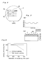
- Fig. 6 shows a case where the form of the monocrystal silicon base-plate is stripe-shaped or dot-shaped in a known manner. It is found out that the superior molten condition is not provided in the case of the stripe-shape.
- an object of the present invention is to provide a method of manufacturing a monocrystal thin film of silicon, which forms the monocrystal thin film controlled in crystal direction, superior in quality through the application of the energy beams.
- the method of manufacturing a monocrystal thin-film of the present invention comprised the successive steps of claim 1. Further embodiments can be found in the dependent claims 2 to 4.
- the size of the insulating film opening-portion is 4 ⁇ m square (or 4 ⁇ m in diameter) or less and the insulating film opening-portion should be filled in advance with the same material as the material to be mono-crystallized.
- the temperature is likely to rise in the non-crystalloid or multicrystal thin-film on the insulating film if the thermal conductivity of the film is smaller than the thermal conductivity of the non-crystalloid or multicrystal thin film in the monocrystal silicon base-plate exposed portion.
- the exposed portion of the monocrystal silicon base-plate is stripe-shaped or becomes more than 4 ⁇ m square, the amount of the heat that escapes to the base plate through the non-crystalloid or multicrystal thin-film within the insulating-film opening portion therein becomes large so that the non-crystalloid or multicrystal thin-film on the opening portion becomes hard to melt.
- the power density of the energy beams is raised till the non-crystalloid or multicrystal thin film within the opening portion is melted, scattering is caused in the non-crystalloid or multicrystal thin-film on the insulating film.
- the configuration of the insulating-film opening portion is made square or almost circular in dot shape and the size thereof is made 4 ⁇ m or lower, so that the amount of heat escaping into the base plate through the opening portion becomes smaller, the difference between the temperature of the non-crystalloid or multicrystal thin-film on the opening portion and the temperature of the non-crystalloid or multicrystal thin-film on the insulating film becomes smaller through the thermal conduction from the periphery to simultaneously melt both portions of the above non-crystalloids or multicrystal thin-films without scattering.
- the insulating-film opening portion is filled in advance with a piece of the non-crystalloid or multicrystal thin film.
- the molten thin-film flows into the insulating film opening portion from the periphery of the opening portion during the application of the energy beams to prevent the non-crystalloid or multicrystal thin-film from becoming thinner so that the crystal growth of the monocrystal thin-film is caused continuously onto the insulating film from on the insulating film opening portion.
- the monocrystals may grow from the monocrystal silicon base-plate exposed portion stably if the insulating film increases in thickness through the above-described operation.
- an insulating film 2 of non-crystal is formed on a top plane of a (100) monocrystal silicon base-plate 1 being partially exposed to provide an exposed portion 1a, as shown in Fig. 1(b), of the monocrystal silicon base-plate 1, as shown in Fig. 1(a).
- the size of the monocrystal silicon base-plate exposed portion is assumed to be 3 ⁇ m square.
- the SiO2 film of 2 ⁇ m in thickness is formed on the monocrystal silicon base-plate 1 by means of, for example, a known thermal oxidation method.
- the monocrystal silicon base-plate 1 of the SiO2 film is selectively by a known photoeching method only in the portion to be exposed to form a plurality of opening portions 1a, 1a, 1a, ... of dot shapes, each being 3 ⁇ m square with an interval of 15 ⁇ m, as shown in Fig. 2.
- the non-crystalloid silicon thin-film or multicrystal silicon thin-film is formed by a known LPCVD method on the whole surface of the insulating film 2 including the opening portion 1a therein.
- organic application film material is applied evenly on the whole surface of the non-crystalloid or multicrystal silicon thin-film, which is formed unevenly on the surface corresponding to the opening portion 1a of the monocrystal silicon base-plate 1 and the surface of the insulating film 2, to form an organic application film.
- equal-speed etching is performed from the surface of the organic application film surface to transfer the even surface of the initial organic application film, and the etching operation is stopped in a time point when the insulating film 2 has been exposed filling the non-crystalloid or multicrystal silicon thin-film 3 into the opening portion 1a of the insulating film 2, as shown in Fig. 1(c).
- the step difference in surface between the non-crystalloid or multicrystal silicon thin film 3 filled in at this time, and the insulating film 2 is assumed to be 1 ⁇ m or less.
- a non-crystalloid or multicrystal silicon thin film 4 which becomes an active layer of 0.6 ⁇ m in thickness is formed by the LPCVD method on both regions by the upper portion of the thin film 3 filled in and of the upper portion of the insulating film 2, as shown in Fig. 1(d).
- an SiO2 film which serves as a surface protective film, i.e., anti-reflective film 5 for the silicon thin film 4 is formed by the APCVD method 850 ⁇ in thickness on the whole surface of the silicon thin film 4, as shown in Fig. 1(e).
- a bundle of laser beams 6 of 60 ⁇ m in molten width and 10W in power is applied upon the region including the monocrystal silicon base-plate exposed portion 1a, as shown in Fig. 1(f), and the mono-crystalloid or multicrystal thin-film 4 on the monocrystal silicon base-plate exposed portion 1a is caused to mono-crystallize with the monocrystal silicon base-plate exposed portion 1a which is adapted as a seed for mono-crystal, so that the monocrystal thin-film 7 is obtained in the crystal direction in coincidence with that of the monocrystal silicon base-plate 1.
- the non-crystalloid or multicrystal silicon thin film 8 is formed 0.6 ⁇ m in thickness by the LPCVD method on the surface protective film 5, and is made stripe-shaped through the selective etching operation by a known photo-etching method.
- each stripe of the non-crystalloid or multicrystal silicon thin film 8 is formed to cover the monocrystal silicon base-plate exposed portion 1a with the width of stripe being 10 ⁇ m, the internal between the stripes being 5 ⁇ m.
- the scanning operation of the laser beam 9 of 60 ⁇ m in molten width and 12 W in power is effected from the monocrystal silicon base-plate exposed portion 1a with the scanning speed of 100 mm per second in the longitudinal direction of the stripe-shaped non-crystalloid or multicrystal silicon thin-film 8, as shown in Fig. 1(i), to provide a monocrystal silicon thin film 10 in which the non-crystalloid or multicrystal silicon thin-film 4 is mono-crystallized with the filled silicon 7 coincided with the monocrystal silicon base-plate 1 in the crystal direction being provided as the seed.
- the monocrystal silicon (100) thin-film 10 coincided (100) with the monocrystal silicon (100) base-plate 1 in the crystal direction is finally obtained on the surface of the insulating film 2.
- the reason why the stripe-shaped non-crystalloid or multicrystal silicon thin-film 8 is formed is that the reflection factor, i.e., reflectivity of the laser beam 9 in the place where the stripe-shaped silicon is located is enlarged compared to that where the stripe-shaped silicon does not exist, as shown in Fig. 3(a), the solidification for monocrystallization starts from right under the stripe-shaped silicon central portion with such temperature distribution being provided, as shown in Fig. 3(b), and the monocrystal growth of the silicon thin film 10 is caused with the monocrystal silicon base-plate exposed portion 1a as the seed.
- the seeding factor of the seed is changed by the insulating film 2 thickness when the size of the insulating film opening portion 1a is changed is examined for comparison, with a result as shown in Fig. 4.
- the opening of the opening portion 1a is as large as 5 ⁇ m square
- the seeding factor is lowered if the insulating film 2 becomes as thick as 4 ⁇ m.
- the seeding factor is not seen if the thickness of the insulating 2 film is made 4 ⁇ m.
- the opening portion 1a will do well if it is made 4 ⁇ m square or less in size, because the thickness between the respective active layers is about 4 ⁇ m even at the largest.
- the reason why the crystal face of the (100) is used as the monocrystal silicon base-plate 1, and the laser scanning direction is made along the ⁇ 010 ⁇ is that the crystal defect is hardest to have in the combination of (100) and (010), and the monocrystal region may be smoothly enlarged from the seed portion.
- the length for which the monocrystal region extends from the seed portion when the laser scanning direction is varied between (010) and (011) by the use of the (100) monocrystal silicon base plate 1 is used as shown in Fig. 5. It is the most desirable from Fig. 5 that the laser scanning in the ⁇ 010 ⁇ direction is best.
- the superior monocrystal silicon thin-film 10 coincided with the monocrystal silicon base plate in the crystal direction is formed on the insulating film 2 even if the insulating film as thick as 4 ⁇ m is sufficiently covered between the active layers of the three-dimensional circuit element on the monocrystal silicon base plate 1.
Landscapes
- Engineering & Computer Science (AREA)
- Physics & Mathematics (AREA)
- Condensed Matter Physics & Semiconductors (AREA)
- General Physics & Mathematics (AREA)
- Manufacturing & Machinery (AREA)
- Computer Hardware Design (AREA)
- Microelectronics & Electronic Packaging (AREA)
- Power Engineering (AREA)
- Chemical & Material Sciences (AREA)
- Crystallography & Structural Chemistry (AREA)
- Optics & Photonics (AREA)
- Recrystallisation Techniques (AREA)
Description
- The present invention relates to a method of manufacturing a monocrystal thin-film to be used in a field where a semiconductor device is manufactured, and more particularly, to improvements in a method of performing the monocrystallizing operation, i.e., single crystallizing operation through the application of energy beams upon the non-monocrystal thin-film of non-crystalloid, i.e., amorphous or ., polycrystals formed on the non-crystalloid insulation film.
- Journal of the Electrochemical Society 132, 8. August 1985, page 119-129 discloses a method of silicon thin film single crystal production on oxidized {100} = (001) silicon wafers supplied with an opening portion, or seeding windows, and a polysilicon film deposited on the surface, including the opening portion. The use of energy beams on the non-monocrystal silicon film is indicated in Fig. 1 and the growth of single crystal by application of the beam in the <100> direction is also in Fig. 1 and the text on page 1920, first paragraph.
- Conventionally, a method of manufacturing a monocrystal thin film with monocrystal silicon base plate coinciding in the crystal direction therewith is proposed through forming a non-crystalloid or multicrystal thin film on an insulating film formed on the monocrystal silicon base-plate, i.e., substrate, and through performing molten-recrystallizing operation by the application of energy beams on the thin film.
- According to the conventional method, when the insulating film is increased in thickness between the monocrystal silicon base-plate and the non-crystalloid or multicrystal thin film to be monocrystallized, the monocrystalloid or multicrystal thin film near the insulating film flows into the insulating film when it is melted through the application of the energy beams to make the non-crystalloid or multicrystal thin-film thinner near the insulating film. Thus, the crystal growth is not continuously caused from the non-crystalloid or multi-crystal thin film in the region which is in contact against the monocrystal silicon base-plate into the non-crystalloid or multicrystal thin film on the insulating film.
- Also, when the insulating film increases in thickness with the monocrystal silicon base-plate being stripe-shaped in form, the monocrystal silicon base-plate and the base plate on the insulating plate are largely different in thermal conduction. The considerable temperature difference is caused in the non-crystalloid or multicrystal thin-film during the application of the energy beams so that the superior monocrystal thin film is not provided. Fig. 6 shows a case where the form of the monocrystal silicon base-plate is stripe-shaped or dot-shaped in a known manner. It is found out that the superior molten condition is not provided in the case of the stripe-shape.
- Accordingly, an object of the present invention is to provide a method of manufacturing a monocrystal thin film of silicon, which forms the monocrystal thin film controlled in crystal direction, superior in quality through the application of the energy beams.
- For the solution of the conventional problems, the method of manufacturing a monocrystal thin-film of the present invention comprised the successive steps of
claim 1. Further embodiments can be found in thedependent claims 2 to 4. The region, where the monocrystal silicon base-plate covered with the non-crystalloid insulating film is exposed, rectangular or almost circular in dot-shape, followed by scanning the energy beams onto the region from the monocrystal silicon base-plate exposed portion of the non-crystalloid or multi-crystal thin-film continuously formed on the mono-crystalloid silicon base-plate exposed portion and the insulating film to provide the monocrystal thin-film coinciding with the monocrystal silicon base-plate in the crystal direction. - Also, it is preferable that the size of the insulating film opening-portion is 4 µm square (or 4 µm in diameter) or less and the insulating film opening-portion should be filled in advance with the same material as the material to be mono-crystallized.
- When the energy beams are applied upon the monocrystalloid or multicrystal thin-film on the insulating film and upon the non-crystalloid or multicrystal thin-film on the non-crystalloid or multicrystal thin-film buried in the monocrystal silicon base-plate exposed portion, the temperature is likely to rise in the non-crystalloid or multicrystal thin-film on the insulating film if the thermal conductivity of the film is smaller than the thermal conductivity of the non-crystalloid or multicrystal thin film in the monocrystal silicon base-plate exposed portion. When the exposed portion of the monocrystal silicon base-plate is stripe-shaped or becomes more than 4 µm square, the amount of the heat that escapes to the base plate through the non-crystalloid or multicrystal thin-film within the insulating-film opening portion therein becomes large so that the non-crystalloid or multicrystal thin-film on the opening portion becomes hard to melt. When the power density of the energy beams is raised till the non-crystalloid or multicrystal thin film within the opening portion is melted, scattering is caused in the non-crystalloid or multicrystal thin-film on the insulating film. Such a problem as described hereinabove become more considerable when the insulating film to be formed on the monocrystal silicon base-plate becomes thicker. In the three-dimension circuit element with elements such as transistors or the like being layer-built into many layers, the insulating film thickness between the respective achieve layers becomes as thick as 2 through 4 µm or more.
- In the present invention, the configuration of the insulating-film opening portion is made square or almost circular in dot shape and the size thereof is made 4 µm or lower, so that the amount of heat escaping into the base plate through the opening portion becomes smaller, the difference between the temperature of the non-crystalloid or multicrystal thin-film on the opening portion and the temperature of the non-crystalloid or multicrystal thin-film on the insulating film becomes smaller through the thermal conduction from the periphery to simultaneously melt both portions of the above non-crystalloids or multicrystal thin-films without scattering.
- Also, the insulating-film opening portion is filled in advance with a piece of the non-crystalloid or multicrystal thin film. The molten thin-film flows into the insulating film opening portion from the periphery of the opening portion during the application of the energy beams to prevent the non-crystalloid or multicrystal thin-film from becoming thinner so that the crystal growth of the monocrystal thin-film is caused continuously onto the insulating film from on the insulating film opening portion.
- Accordingly, the monocrystals may grow from the monocrystal silicon base-plate exposed portion stably if the insulating film increases in thickness through the above-described operation.
- These and other objects and features of the present invention will become apparent from the following description taken in conjunction with the preferred embodiment thereof with reference to the accompanying drawings, in which:
- Figs. 1(a) through 1(i) are respectively process charts showing sample sections for illustrating a method of manufacturing monocrystal thin-film in accordance with one embodiment of the present invention;
- Fig. 2 is a view for illustrating the forming direction, i.e., crystal growth direction, of the stripe-shaped thin film on the application of the method of the present invention;
- Figs. 3(a) and 3(b) show a principle chart for illustrating a method of controlling the reflection factor to provide the given temperature distribution to be employed in the method of the present invention;
- Fig. 4 is a chart showing the influences of the size of the insulating-film opening portion applies upon the seeding factor in the method of the present invention;
- Fig. 5 is a chart showing the relationship between the laser scanning direction and the length of the monocrystal wherein the monocrystal region is enlarged from the seed portion to be employed in the method of the present invention; and
- Figs. 6(a) and 6(b) show views for illustrating the molten condition between the dot shape and the stripe shape in the form of the insulating-film on the employment of a conventional method.
- Referring now to the drawings, there are shown process charts for illustrating one embodiment of the present invention in Figs. 1 (a) through 1(i).
- First, an
insulating film 2 of non-crystal is formed on a top plane of a (100) monocrystal silicon base-plate 1 being partially exposed to provide an exposedportion 1a, as shown in Fig. 1(b), of the monocrystal silicon base-plate 1, as shown in Fig. 1(a). At this time, the size of the monocrystal silicon base-plate exposed portion is assumed to be 3 µm square. Firstly, the SiO₂ film of 2 µm in thickness is formed on the monocrystal silicon base-plate 1 by means of, for example, a known thermal oxidation method. Thereafter, the monocrystal silicon base-plate 1 of the SiO₂ film is selectively by a known photoeching method only in the portion to be exposed to form a plurality ofopening portions - Then, a piece of non-crystalloid or multicrystal silicon
thin film 3 which is almost equal in thickness to theinsulating film 2, as shown in Fig. 1(c), is embedded only into the exposedportion 1a of the monocrystal silicon base-plate 1 provided in and surrounded by theinsulating film 2. Concretely, the non-crystalloid silicon thin-film or multicrystal silicon thin-film is formed by a known LPCVD method on the whole surface of theinsulating film 2 including theopening portion 1a therein. Then, organic application film material is applied evenly on the whole surface of the non-crystalloid or multicrystal silicon thin-film, which is formed unevenly on the surface corresponding to theopening portion 1a of the monocrystal silicon base-plate 1 and the surface of theinsulating film 2, to form an organic application film. Thereafter, equal-speed etching is performed from the surface of the organic application film surface to transfer the even surface of the initial organic application film, and the etching operation is stopped in a time point when theinsulating film 2 has been exposed filling the non-crystalloid or multicrystal silicon thin-film 3 into theopening portion 1a of theinsulating film 2, as shown in Fig. 1(c). - It is to be noted that, upon the completion of the etching, the step difference in surface between the non-crystalloid or multicrystal silicon
thin film 3 filled in at this time, and theinsulating film 2 is assumed to be 1 µm or less. - Then, a non-crystalloid or multicrystal silicon
thin film 4 which becomes an active layer of 0.6 µm in thickness is formed by the LPCVD method on both regions by the upper portion of thethin film 3 filled in and of the upper portion of theinsulating film 2, as shown in Fig. 1(d). Then, an SiO₂ film which serves as a surface protective film, i.e.,anti-reflective film 5 for the siliconthin film 4 is formed by the APCVD method 850 Å in thickness on the whole surface of the siliconthin film 4, as shown in Fig. 1(e). - Next, a bundle of laser beams 6 of 60 µm in molten width and 10W in power is applied upon the region including the monocrystal silicon base-plate exposed
portion 1a, as shown in Fig. 1(f), and the mono-crystalloid or multicrystal thin-film 4 on the monocrystal silicon base-plate exposedportion 1a is caused to mono-crystallize with the monocrystal silicon base-plate exposedportion 1a which is adapted as a seed for mono-crystal, so that the monocrystal thin-film 7 is obtained in the crystal direction in coincidence with that of the monocrystal silicon base-plate 1. - Then, a non-crystalloid or multicrystal silicon thin-
film 8 of stripe-shape on the surface of the surfaceprotective film 5, as shown in Figs. 1(g) and 1(h) such that the longitudinal direction of the stripe may become 〈010〉 of the monocrystalsilicon base plate 1, as shown in Fig. 2. Concretely, the non-crystalloid or multicrystal siliconthin film 8 is formed 0.6 µm in thickness by the LPCVD method on the surfaceprotective film 5, and is made stripe-shaped through the selective etching operation by a known photo-etching method. At this time, each stripe of the non-crystalloid or multicrystal siliconthin film 8 is formed to cover the monocrystal silicon base-plate exposedportion 1a with the width of stripe being 10 µm, the internal between the stripes being 5 µm. - Finally, the scanning operation of the laser beam 9 of 60 µm in molten width and 12 W in power is effected from the monocrystal silicon base-plate exposed
portion 1a with the scanning speed of 100 mm per second in the longitudinal direction of the stripe-shaped non-crystalloid or multicrystal silicon thin-film 8, as shown in Fig. 1(i), to provide a monocrystal siliconthin film 10 in which the non-crystalloid or multicrystal silicon thin-film 4 is mono-crystallized with the filledsilicon 7 coincided with the monocrystal silicon base-plate 1 in the crystal direction being provided as the seed. With the above process, the monocrystal silicon (100) thin-film 10 coincided (100) with the monocrystal silicon (100) base-plate 1 in the crystal direction is finally obtained on the surface of theinsulating film 2. It is to be noted that the reason why the stripe-shaped non-crystalloid or multicrystal silicon thin-film 8 is formed is that the reflection factor, i.e., reflectivity of the laser beam 9 in the place where the stripe-shaped silicon is located is enlarged compared to that where the stripe-shaped silicon does not exist, as shown in Fig. 3(a), the solidification for monocrystallization starts from right under the stripe-shaped silicon central portion with such temperature distribution being provided, as shown in Fig. 3(b), and the monocrystal growth of the siliconthin film 10 is caused with the monocrystal silicon base-plate exposedportion 1a as the seed. - How the seeding factor of the seed is changed by the
insulating film 2 thickness when the size of the insulatingfilm opening portion 1a is changed is examined for comparison, with a result as shown in Fig. 4. When the opening of theopening portion 1a is as large as 5 µm square, the seeding factor is lowered if theinsulating film 2 becomes as thick as 4 µm. Also, when it is 2 µm, 3 µm or 4 µm square, the seeding factor is not seen if the thickness of the insulating 2 film is made 4 µm. In the three-dimensional circuit element, theopening portion 1a will do well if it is made 4 µm square or less in size, because the thickness between the respective active layers is about 4 µm even at the largest. - Also, it is to be noted that the reason why the crystal face of the (100) is used as the monocrystal silicon base-
plate 1, and the laser scanning direction is made along the 〈010〉 is that the crystal defect is hardest to have in the combination of (100) and (010), and the monocrystal region may be smoothly enlarged from the seed portion. The length for which the monocrystal region extends from the seed portion when the laser scanning direction is varied between (010) and (011) by the use of the (100) monocrystalsilicon base plate 1 is used as shown in Fig. 5. It is the most desirable from Fig. 5 that the laser scanning in the 〈010〉 direction is best. - As is clear from the foregoing description, according to the present invention, the superior monocrystal silicon thin-
film 10 coincided with the monocrystal silicon base plate in the crystal direction is formed on theinsulating film 2 even if the insulating film as thick as 4 µm is sufficiently covered between the active layers of the three-dimensional circuit element on the monocrystalsilicon base plate 1.
Claims (4)
- A method of manufacturing a monocrystal thin-film of silicon comprising the successive steps of forming a non-crystalline insulating film on a mono-crystal silicon base-plate, providing a dot shaped opening in the insulating film so that the corresponding portion of the monocrystal silicon base plate is exposed,
filling the dot-shaped opening of the insulating-film with a non-monocrystalline silicon thin-film,
forming a non-monocrystalline thin-film of silicon on said non-crystalline insulating film,
forming an anti-reflective film on said non-monocrystal thin-film,
applying energy beams upon the region including the dot shaped opening filled with the said non-monocrystalline silicon thin film to turn it into a monocrystal thin-film coinciding with the monocrystal silicon base-plate in crystal direction with the exposed portion of said monocrystal silicon base-plate provided as the seed,
forming a stripe-shaped silicon reflection enhancing film on said anti reflective film so that said monocrystallized region is included, and
applying energy beams in the stripe direction to monocrystallize said non-monocrystalline silicon thin-film formed on the insulating film with the monocrystallized film in the dot shaped opening being provided as the seed. - A method in accordance with claim 1, wherein the size of the dot-shaped opening is 4 µm or lower.
- A method in accordance with claim 2, wherein the monocrystal silicon base-plate exposed portion which become the seed portion is multiply formed and a plurality of stripe-shaped silicon covered films are formed in accordance with said plurality of seed portions.
- A method in accordance with claims 1 to 3, wherein the orientation of the monocrystal silicon base-plate is {100}, and the direction of the stripe-shaped silicon covered film is <100>.
Applications Claiming Priority (6)
| Application Number | Priority Date | Filing Date | Title |
|---|---|---|---|
| JP28543885A JPS62145721A (en) | 1985-12-20 | 1985-12-20 | Manufacture of single crystal thin film |
| JP285438/85 | 1985-12-20 | ||
| JP68554/86 | 1986-03-28 | ||
| JP6855486A JPS62226621A (en) | 1986-03-28 | 1986-03-28 | Forming method for single crystal silicon thin film |
| JP225900/86 | 1986-09-26 | ||
| JP22590086A JPS6381807A (en) | 1986-09-26 | 1986-09-26 | Manufacture of single crystal silicon thin film |
Publications (3)
| Publication Number | Publication Date |
|---|---|
| EP0227076A2 EP0227076A2 (en) | 1987-07-01 |
| EP0227076A3 EP0227076A3 (en) | 1989-05-24 |
| EP0227076B1 true EP0227076B1 (en) | 1992-06-17 |
Family
ID=27299781
Family Applications (1)
| Application Number | Title | Priority Date | Filing Date |
|---|---|---|---|
| EP86117799A Expired - Lifetime EP0227076B1 (en) | 1985-12-20 | 1986-12-19 | Method of manufacturing monocrystal thin-film |
Country Status (3)
| Country | Link |
|---|---|
| US (1) | US4801351A (en) |
| EP (1) | EP0227076B1 (en) |
| DE (1) | DE3685732T2 (en) |
Families Citing this family (5)
| Publication number | Priority date | Publication date | Assignee | Title |
|---|---|---|---|---|
| JPS62206816A (en) * | 1986-03-07 | 1987-09-11 | Agency Of Ind Science & Technol | Manufacture of semiconductor crystal layer |
| DE3779672T2 (en) * | 1986-03-07 | 1993-01-28 | Iizuka Kozo | METHOD FOR PRODUCING A MONOCRISTALLINE SEMICONDUCTOR LAYER. |
| US4931323A (en) * | 1987-12-10 | 1990-06-05 | Texas Instruments Incorporated | Thick film copper conductor patterning by laser |
| FR2640428B1 (en) * | 1988-12-09 | 1992-10-30 | Thomson Csf | METHOD OF HARDENING WITH RESPECT TO IONIZING RADIATION OF ACTIVE ELECTRONIC COMPONENTS, AND HARDENED COMPONENTS OF LARGE DIMENSIONS |
| TW264575B (en) * | 1993-10-29 | 1995-12-01 | Handotai Energy Kenkyusho Kk |
Family Cites Families (10)
| Publication number | Priority date | Publication date | Assignee | Title |
|---|---|---|---|---|
| JPS5734331A (en) * | 1980-08-11 | 1982-02-24 | Toshiba Corp | Manufacture of semiconductor device |
| US4487639A (en) * | 1980-09-26 | 1984-12-11 | Texas Instruments Incorporated | Localized epitaxy for VLSI devices |
| US4448632A (en) * | 1981-05-25 | 1984-05-15 | Mitsubishi Denki Kabushiki Kaisha | Method of fabricating semiconductor devices |
| US4565599A (en) * | 1981-12-21 | 1986-01-21 | Massachusetts Institute Of Technology | Graphoepitaxy by encapsulation |
| JPS58130517A (en) * | 1982-01-29 | 1983-08-04 | Hitachi Ltd | Manufacture of single crystal thin film |
| JPS59108313A (en) * | 1982-12-13 | 1984-06-22 | Mitsubishi Electric Corp | Manufacture of semiconductor single crystal layer |
| CA1197628A (en) * | 1984-01-05 | 1985-12-03 | Thomas W. Macelwee | Fabrication of stacked mos devices |
| US4555300A (en) * | 1984-02-21 | 1985-11-26 | North American Philips Corporation | Method for producing single crystal layers on insulators |
| FR2580672B1 (en) * | 1985-04-19 | 1987-05-15 | France Etat | METHOD FOR MANUFACTURING ON AN INSULATING SUPPORT OF A SINGLE-CRYSTAL, LOCAL-DEFECT SILICON FILM |
| US4651407A (en) * | 1985-05-08 | 1987-03-24 | Gte Laboratories Incorporated | Method of fabricating a junction field effect transistor utilizing epitaxial overgrowth and vertical junction formation |
-
1986
- 1986-12-19 EP EP86117799A patent/EP0227076B1/en not_active Expired - Lifetime
- 1986-12-19 US US06/943,428 patent/US4801351A/en not_active Expired - Lifetime
- 1986-12-19 DE DE8686117799T patent/DE3685732T2/en not_active Expired - Fee Related
Also Published As
| Publication number | Publication date |
|---|---|
| EP0227076A2 (en) | 1987-07-01 |
| DE3685732T2 (en) | 1993-01-21 |
| US4801351A (en) | 1989-01-31 |
| DE3685732D1 (en) | 1992-07-23 |
| EP0227076A3 (en) | 1989-05-24 |
Similar Documents
| Publication | Publication Date | Title |
|---|---|---|
| EP0077020B1 (en) | Method of manufacturing single-crystal film | |
| EP0235819B1 (en) | Process for producing single crystal semiconductor layer | |
| US4670088A (en) | Lateral epitaxial growth by seeded solidification | |
| US4596604A (en) | Method of manufacturing a multilayer semiconductor device | |
| US4576851A (en) | Semiconductor substrate | |
| US4523962A (en) | Method for fabricating monocrystalline semiconductor layer on insulating layer by laser crystallization using a grid of anti-reflection coating disposed on poly/amorphous semiconductor | |
| US4599133A (en) | Method of producing single-crystal silicon film | |
| EP0070878B1 (en) | Growth of structures based on group iv semiconductor materials | |
| EP0227076B1 (en) | Method of manufacturing monocrystal thin-film | |
| EP0236953B1 (en) | Method of manufacturing semiconductor crystalline layer | |
| KR20000021215A (en) | Thin film transistor using a method of crystallizing a silicon thin film and a method thereof | |
| US4576676A (en) | Thick crystalline films on foreign substrates | |
| JPH027415A (en) | Formation of soi thin film | |
| US5094714A (en) | Wafer structure for forming a semiconductor single crystal film | |
| EP0575965A2 (en) | Method of forming semiconductor crystal and semiconductor device | |
| Biegelsen et al. | Laser induced crystal growth of silicon islands on amorphous substrates | |
| JPS6083322A (en) | Crystallizing method of semiconductor thin-film | |
| JPH0442358B2 (en) | ||
| JPS627116A (en) | Manufacture of soi single crystal | |
| JPS62179112A (en) | Formation of soi structure | |
| JPS62145721A (en) | Manufacture of single crystal thin film | |
| JPS58180019A (en) | Semiconductor base body and its manufacture | |
| JPH024559B2 (en) | ||
| JPH04214615A (en) | Manufacture of semiconductor device | |
| JPH0652711B2 (en) | Semiconductor device |
Legal Events
| Date | Code | Title | Description |
|---|---|---|---|
| PUAI | Public reference made under article 153(3) epc to a published international application that has entered the european phase |
Free format text: ORIGINAL CODE: 0009012 |
|
| 17P | Request for examination filed |
Effective date: 19861219 |
|
| AK | Designated contracting states |
Kind code of ref document: A2 Designated state(s): DE FR GB |
|
| PUAL | Search report despatched |
Free format text: ORIGINAL CODE: 0009013 |
|
| AK | Designated contracting states |
Kind code of ref document: A3 Designated state(s): DE FR GB |
|
| RHK1 | Main classification (correction) |
Ipc: H01L 21/268 |
|
| 17Q | First examination report despatched |
Effective date: 19910131 |
|
| GRAA | (expected) grant |
Free format text: ORIGINAL CODE: 0009210 |
|
| AK | Designated contracting states |
Kind code of ref document: B1 Designated state(s): DE FR GB |
|
| REF | Corresponds to: |
Ref document number: 3685732 Country of ref document: DE Date of ref document: 19920723 |
|
| ET | Fr: translation filed | ||
| PLBE | No opposition filed within time limit |
Free format text: ORIGINAL CODE: 0009261 |
|
| STAA | Information on the status of an ep patent application or granted ep patent |
Free format text: STATUS: NO OPPOSITION FILED WITHIN TIME LIMIT |
|
| 26N | No opposition filed | ||
| PGFP | Annual fee paid to national office [announced via postgrant information from national office to epo] |
Ref country code: GB Payment date: 19961210 Year of fee payment: 11 |
|
| PGFP | Annual fee paid to national office [announced via postgrant information from national office to epo] |
Ref country code: FR Payment date: 19961227 Year of fee payment: 11 Ref country code: DE Payment date: 19961227 Year of fee payment: 11 |
|
| PG25 | Lapsed in a contracting state [announced via postgrant information from national office to epo] |
Ref country code: GB Free format text: LAPSE BECAUSE OF NON-PAYMENT OF DUE FEES Effective date: 19971219 |
|
| PG25 | Lapsed in a contracting state [announced via postgrant information from national office to epo] |
Ref country code: FR Free format text: THE PATENT HAS BEEN ANNULLED BY A DECISION OF A NATIONAL AUTHORITY Effective date: 19971231 |
|
| GBPC | Gb: european patent ceased through non-payment of renewal fee |
Effective date: 19971219 |
|
| PG25 | Lapsed in a contracting state [announced via postgrant information from national office to epo] |
Ref country code: DE Free format text: LAPSE BECAUSE OF NON-PAYMENT OF DUE FEES Effective date: 19980901 |
|
| REG | Reference to a national code |
Ref country code: FR Ref legal event code: ST |