EP0227044B1 - Optical disc apparatus - Google Patents
Optical disc apparatus Download PDFInfo
- Publication number
- EP0227044B1 EP0227044B1 EP86117653A EP86117653A EP0227044B1 EP 0227044 B1 EP0227044 B1 EP 0227044B1 EP 86117653 A EP86117653 A EP 86117653A EP 86117653 A EP86117653 A EP 86117653A EP 0227044 B1 EP0227044 B1 EP 0227044B1
- Authority
- EP
- European Patent Office
- Prior art keywords
- optical disc
- voltage
- data
- output
- circuit
- Prior art date
- Legal status (The legal status is an assumption and is not a legal conclusion. Google has not performed a legal analysis and makes no representation as to the accuracy of the status listed.)
- Expired
Links
Images
Classifications
-
- G—PHYSICS
- G11—INFORMATION STORAGE
- G11B—INFORMATION STORAGE BASED ON RELATIVE MOVEMENT BETWEEN RECORD CARRIER AND TRANSDUCER
- G11B7/00—Recording or reproducing by optical means, e.g. recording using a thermal beam of optical radiation by modifying optical properties or the physical structure, reproducing using an optical beam at lower power by sensing optical properties; Record carriers therefor
- G11B7/08—Disposition or mounting of heads or light sources relatively to record carriers
- G11B7/09—Disposition or mounting of heads or light sources relatively to record carriers with provision for moving the light beam or focus plane for the purpose of maintaining alignment of the light beam relative to the record carrier during transducing operation, e.g. to compensate for surface irregularities of the latter or for track following
- G11B7/095—Disposition or mounting of heads or light sources relatively to record carriers with provision for moving the light beam or focus plane for the purpose of maintaining alignment of the light beam relative to the record carrier during transducing operation, e.g. to compensate for surface irregularities of the latter or for track following specially adapted for discs, e.g. for compensation of eccentricity or wobble
- G11B7/0953—Disposition or mounting of heads or light sources relatively to record carriers with provision for moving the light beam or focus plane for the purpose of maintaining alignment of the light beam relative to the record carrier during transducing operation, e.g. to compensate for surface irregularities of the latter or for track following specially adapted for discs, e.g. for compensation of eccentricity or wobble to compensate for eccentricity of the disc or disc tracks
-
- G—PHYSICS
- G11—INFORMATION STORAGE
- G11B—INFORMATION STORAGE BASED ON RELATIVE MOVEMENT BETWEEN RECORD CARRIER AND TRANSDUCER
- G11B7/00—Recording or reproducing by optical means, e.g. recording using a thermal beam of optical radiation by modifying optical properties or the physical structure, reproducing using an optical beam at lower power by sensing optical properties; Record carriers therefor
- G11B7/08—Disposition or mounting of heads or light sources relatively to record carriers
- G11B7/085—Disposition or mounting of heads or light sources relatively to record carriers with provision for moving the light beam into, or out of, its operative position or across tracks, otherwise than during the transducing operation, e.g. for adjustment or preliminary positioning or track change or selection
- G11B7/08505—Methods for track change, selection or preliminary positioning by moving the head
-
- G—PHYSICS
- G05—CONTROLLING; REGULATING
- G05B—CONTROL OR REGULATING SYSTEMS IN GENERAL; FUNCTIONAL ELEMENTS OF SUCH SYSTEMS; MONITORING OR TESTING ARRANGEMENTS FOR SUCH SYSTEMS OR ELEMENTS
- G05B2219/00—Program-control systems
- G05B2219/30—Nc systems
- G05B2219/49—Nc machine tool, till multiple
- G05B2219/49177—Runout, eccentricity, unbalance of tool or workpiece
Definitions
- the present invention relates to an optical disc apparatus which carries out recording or reproducing of information by the tracking of an optical head with respect to a rotating optical disc, and more particularly to an eccentricity correction means of the optical disc.
- an optical disc has concentric circular or spiral recording tracks as information recording medium, and the recording or reproducing of information for the recording track of the optical disc is carried out by linearly moving the recording head in the radial direction of the optical disc while rotating the disc.
- the optical head has to precisely follow the recording tracks of the rotating disc. For this reason, tracking control is ordinarily carried out by using a tracking servo system.
- the optical disc apparatus of the above description when the optical head is moved from an arbitrary recording track which is in rotation to another recording track, tracking is interrupted for a while to move the optical head for a distance which corresponds to the separation between the present and desired tracks, and tracking is resumed.
- the recording tracks themselves of the optical disc are in general not necessarily concentric with respect to the center of the rotation shaft of the motor that drives to rotate the optical disc, and are often eccentric. Because of this, when tracking is interrupted once, the relative position of the optical head with respect to the recording track has a dispersion that corresponds to the eccentricity amount so that when tracking is resumed after the head has been moved, it leads to a drawback that accuracy tends to be lowered by the deviation corresponding to the dispersion. This results in a difficulty in reducing the time for positioning the optical head to the desired track.
- a spiral pre-groove 2 for tracking on the surface of the substrate, in order to facilitate recording and reproducing. Since the recording track is provided in the pre-groove 2, the portion identical to that of the pre-groove 2 is referred to simply as the track hereinafter.
- the track pitch is drawn schematically with wide separation.
- the real track is formed with a considerably small pitch of the order of ⁇ m.
- the optical disc I is placed on a spindle motor, as will be described later, to be rotated in the direction of the arrow R of Fig. I.
- the beam spot (laser spot) of the optical beam projected from the optical head is traced on the track 2.
- the beam spot is shifted to track 2 by one track outward for each one rotation of the optical disc I.
- Recording of information is made by the change in reflectivity generated by the phase transition or the like in a thin film layer in the track portion of the disc, through irradiation of the beam spot whose intensity is modulated by an information signal.
- Fig. 2 shows a track control device for causing the optical head 4 to follow the track 2 in recording and reproducing information from the optical disc I as in the above.
- a light source is omitted to simplify the track control device.
- reference numeral 5 is an objective lens which lets the beam spot of the light beam to be projected on the optical disc I
- 6 is a driving coil for controlling the position of the objective lens 5 in the radial direction of the optical disc I
- 13a and 13b are photodetector for detecting the intensities of reflected lights BI and 12, respectively, photodetector 13a being connected to the negative input terminal of a differential amplifier 15a via a sensor amplifier 14a while photodetector 13b is connected to the positive input terminal of the differential amplifier 15 via another sensor amplifier 14b.
- the reflected light 21 is reflected from the surface portion of the disc (the area outside the pre-groove 2) with larger intensity, giving larger detected value to the photodetector 13a, and causes the differential amplifier 15 to output a negative track deviation signal voltage - TS.
- the reflected light 12 has a larger intensity opposite to the above, and there is output a positive track deviation signal voltage + TS from the differential amplifier.
- the track control is carried out by applying the positive and negative track deviation signal voltages ⁇ TS to the driving coil 6 and controls the position of the objective 5 to have the track difference signal voltage TS to be zero.
- the beam spot follows the track 2 to carry out the correct recording and reproducing.
- the optical disc apparatus can carry out the operation of repeatedly reproducing an identical track of one turn, the so-called track-on mode, in addition to the ordinary operation of recording and reproducing as in the above.
- the track-on made operation can be realized by applying a jump pulse to the driving coil 6 at the timing when the optical disc I completed one rotation, to cause the beam spot to jump to the adjacent previous track.
- the solid waveform in Fig. 3 is the output waveform of the track deviation signal voltage TS when the track jump is carried out by passing a current in the driving coil in the direction of the arrow in Fig. 2, and the broken-line waveform is the output waveform for the track deviation signal voltage TS when the track jump is carried out in the opposite direction.
- the track deviation signal voltage TS is output as a waveform for one cycle every time when the optical head 2 traverses the pre-groove 2. Therefore, the number of waves in the track deviation signal voltage TS corresponds to the number of tracks jumped.
- the central point Cpl of the optical disc I and the center Cp2 of the rotation shaft of the spindle motor do not coincide perfectly, producing eccentricity for the optical disc I, due to the accuracy of the center hole of the optical disc I, errors generated in chucking the disc to the spindle moter, and so on.
- the beam spot coincides with the track 2a at points a and c, but deviates by the amount of eccentricity at points b and d, where it is shifted to the outside of the track 2a at point b while it is shifted to the inside of the track 2a at point d.
- Fig. 5 shows the waveform of the track difference signal voltage TS on which each of the points a, b, c and d is indicated.
- the track deviation signal voltage TS is applied to the driving coil 6, and the beam spot is corrected to follow the track 2 so as to be moved to the inside at point b and to the outside at point d.
- A/D converter used in the prior art optical disc apparatus which can carry out high precision A/D conversion.
- the A/D converter has a voltage comparison circuit, a successive comparison register, a D/A converter that constitutes the feedback circuit, a clock oscillator which carries out the overall control, and so on.
- a digital quantity which corresponds to the input analog voltage is arranged to be output by the following way. Namely, starting with the least significant bit of the successive comparison register, a converted voltage that corresponds to each one bit is arranged to be output from the D/A converter to compare the converted voltage with the input analog voltage in the voltage comparison circuit. If these two voltages do not coincide, the same procedure is successively repeated for each bit, until agreement is obtained.
- a parallel comparison type A/D converter is known as another existing A/D converter which can carry out A/D conversion at high speed.
- the A/D converter comparises a resistor ladder circuit which generates (2 n- 1) reference voltages by subdividing a given voltage into 2 n equal parts when the digital quantity to be output has n bits, (2 r- l) voltage comparators to each of their reference terminals for setting each of the reference voltages generated in the resistor ladder circuit, and a decoder which transmits the outputs of the voltage comparators as an n-bit digital quantity after binary coding conversion.
- an input analog voltage is input parallel to the input terminals of all of the voltage comparators and compared at once with all of the reference voltages, to output from the decoder a digital quantity that corresponds to the input analog voltage.
- EP-A 0 076 347 describes an optical playback machine which plays back data recorded on an optical record in track segments, employs a track intercept apparatus to transversely deflect a scanning light beam during each scan to accurately intercept each selected track segment despite record or optical misalignment.
- a track intercept control circuit includes storage means for storage of variable values of track alignment data, adjust means for producing an adjustment signal from the stored data and timing means controlling gating circuitry for applying the adjustment signal to a light beam deflection means at the proper point in each scan.
- EP-A 0 162 702 describes a tracking control arrangement for use in an optical disc player comprising a photodetector for receiving a light beam reflected at an optical disc on which an information signal is recorded in a record track, signal generating circuit for generating a reproduced information signal and a tracking error signal from the output of the photodetector, a modifier for modifying the tracking error signal in response to variations in the total quantity of light of the light beam received by the photodetector, driving means for driving an optical device to maintain the light beam in a proper tracking relation to the record track in response to the modified tracking error signal, a detector for detecting a variation in the reproduced information signal resulting from the condition in which the light beam reflected at a blank area in the record track is received by the photodetector and a gain controller for varying the gain of transmission of the modified tracking error signal from the modifier to the driving means in response to a predetermined detection output of the detector.
- An object of the present invention in view of the above circumstances, is to provide an optical disc appratus which enables the optical head to precisely follow the recording track on the optical disc by minimizing the amount of eccentricity between the optical head and the optical disc.
- Another object of the present invention is to provide an eccentricity correction device in the optical disc apparatus which enables a precise track jump.
- Still another object of the present invention is to provide an A/D converter which can carry out high accuracy A/D conversion at high speed.
- an optical disc apparatus including, optical means for recording or reproducing information on the recording track of an optical disc; means for detecting at least deviation amount of beam spot projected from said optical means on the recording track of the optical disc and generating a track deviation signal based on the deviation amount; means for comparing the track deviation signal with a reference signal; and means for converting the digital quantity read from said memory means to an analog signal for driving said optical means, characterized by means for memorizing a first digital quantity; and means for calculating a second digital quantity based on the digital output of the comparison means and the first digital quantity from the memory means and transferring the second digital quantity to the memory means and repeating said calculation of the second digital quantity until the voltage of the track deviation signal become smaller than the voltage of said reference signal.
- the optical disc apparatus in the present invention reads via an A/D converter, the position deviation of tracking output from an optical head, prior to the actual operation of recording or reproducing and stores it as eccentricity correction data after giving a predetermined data processing.
- the eccentricity correction data that has been stored is transferred to a D/A converter and the amount of eccentricity between the optical head and the optical disc is minimized by giving the output of the D/A converter to a tracking control means.
- the voltage comparison circuit there are set a plurality of positive and negative reference voltages related to the weighting of each bit, and by generating an analog voltage proportional to an interim digital quantity stored in the memory in the D/A converter, the difference voltage between the input analog voltage and the generated analog voltage is simultaneously compared with the plurality of reference voltages in the voltage comparison circuit. Based on the output from the voltage comparison circuit, a binary number weighted corresponding to the absolute value of the difference voltage, in response to the positive or negative sign of the difference voltage, is added or subtracted by the adder from the digital quantity read from the memory.
- the new digital quantity obtained in this way as the result of the arithmetic operation is stored in the memory, and the above operation is repeated until the absolute value of the difference voltage becomes smaller than the reference voltage that corresponds to the weighting for the least significant bit. In this manner, high accuracy A/D conversion is arranged to be accomplished at high speed.
- 21 is an optical disc
- 22 is a driving motor for rotating the optical disc
- 23 is an optical head for recording and reproducing.
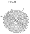
- the optical disc 21 has a concentric circular or spiral recording track 300, as shown in Fig. 8, and one rotation of the optical disc is subdivided into 256 sectors of "0 to 255" for data memory.
- the motor 22 is driven by a motor control circuit 24.
- a laser oscillator 31 is used as a laser beam light generating means, and an objective 35 concentrates beam light on the optical disc 21 and positions the beam light on the recording track.
- a vertical driving coil 36 moves the objective 35 in the vertical direction, the direction of the optical axis, and a radial driving coil 37 moves as a tracking means the objective 35 in the radial direction, the direction orthogonal to the optical axis of the optical disc 21.
- Split beam detectors 41 and 43 carry out photoelectric conversion by receiving reflected light from the optical disc 21.
- the laser oscillator 31 generates laser beam light by oscillation driven by a driving circuit 44.
- the laser oscillator 31 when information is recorded on the recording track of the optical disc 21, the laser oscillator 31 generates laser beam light whose intensity is modulated in response to the information to be recorded, and when information is reproduced from the recording track, the laser oscillator 31 generates laser beam light which has a constant intensity.
- the beam light from the laser oscillator 31 is led, after made into parallel beams of light by a collimator lens 32, to a polarized light beam splitter 33 where it is reflected on the side of the optical disc 21.
- the reflected beam light is led to the objective 35 through a quarter-wavelength plate 34, and is irradiated on the recording track of the optical disc 21 after being made into a spot- like beam light by the focusing of the objective 35.
- the reflected light from the optical disc 21 by this light irradiation is led through the objective 35, the quarter-wavelength plate 34, and the polarized light beam splitter 33 to a half prism 38 where it is split into two systems of light.
- One of the split reflected lights is focused through a condenser 39 and a knife edge 40 on the light-receiving surface of the light detector 41 where it is photoelectrically converted.
- Each of the output signals of the light detector 41 is used for the focusing control.
- the other of the slit reflected lights is focused through a condenser 42 on the light-receiving surface of the light detector 43 where it is photoelectrically converted.
- Each of the output signals of the light detector 43 is used for tracking control and for reading of recorded information as described later.
- Each of the output signals of the light detector 41 is supplied to a differential amplifier 45 from whose output it is arranged to be able to obtain a focus deviation signal of the beam light on the optical disc 21.
- the focus deviation signal output from the differential amplifier 45 is supplied to a focusing control circuit 46.
- the focusing control circuit 46 controls the driving coil 36 for the vertical direction, and carries out focusing control by driving the objective 35 in the vertical direction so as to position the beam light that irradiates the optical disc 21 to be correctly focused all the time.
- Each of the output signals of the light detector 43 is supplied respectively to a differential amplifier 47 whose output is arranged to give a tracking position deviation signal.
- the tracking position deviation signal output of the differential amplifier 47 is supplied respectively to a tracking control circuit 48 as a tracking control means and an A/D converter 49.
- the tracking control circuit 48 controls the driving coil for radial direction 37, and carries out tracking control so as to position the beam light to be on the recording track all the time and the beam light precisely follows the recording track, by driving the objective 35 in the radial direction of the optical disc 21.
- servo mechanism in the state when the tracking is in progress, servo mechanism is on for not only the objective 35 but also the linear motor control circuit 30 to determine the positioning of the beam light by the use of the objective 35 and the linear motor 25.
- the A/D converter 49 outputs the input tracking position deviation signal to a data bus 50 by converting it into a digital signal.
- each output signal of the light detector 43 is supplied respectively to a video circuit 51.
- the video circuit 51 generates a reproduced signal of recorded information, namely, a video signal reflecting bits within the recording track, by adding each output signal of the light detector 43, and outputs the video signal by binary coding it to the data bus 50 as reading information.
- the driving circuit 44 Connected to the data bus 50 are the driving circuit 44, the linear motor control circuit 30, and the motor control circuit 24. Also connected to the data bus 50 are a sector counter 52, a CPU which governs the overall control 53, a ROM 54 storing the operating program of the CPU and the like, a RAM 55 as a memory means for memorizing the eccentricity correction data, and a D/A converter 56.
- the sector counter 52 is actuated by the 256 sector pulses per rotation of the optical disc 21 generated from the motor control circuit 24. A counter simply counts "from 0 to 255,” and the counted value is output to the data bus 50 as well as is supplied to one of the input terminals of the selector 57 as an address signal of the RAM 55.
- the selector 57 operates switching by a hold acknowledge signal from the CPU 53, and its output terminal is connected to the ROM 54 and the RAM 55 via an address bus 58.
- a hold pulse is input from a hold pulse generation circuit 59
- the CPU 53 becomes a held state, and generates a hold acknowledge signal which indicates that it is being held.
- the hold acknowledge signal is supplied to the selector 57, RAM 55, D/A converter 56, and hold pulse generation circuit 59.
- the D/A converter 56 converts the data transferred from the RAM 55 to an analog signal, and supplies the converted output to the tracking control circuit 48 and the linear motor control circuit 30 as bias.
- the hold pulse generation circuit 59 is a latch circuit which is set by the rising of a sector pulse generated from the motor control circuit 24 and reset by a hold acknowledge signal, and generates a hold pulse which becomes high level and low level in response to the set and reset, respectively.
- a course access for moving the beam spot is gained by reading position information recorded in advance in the recording track of the optical disc 21 and moving the optical head 23 by the linear motor 25 to the vicinity of the target recording track. Then, by carrying out a precision access by using the objective 35, it becomes possible to move the beam light to the desired recording track. These operations are carried out by the control of the CPU 53. Since such an access operation is already well known, further explanation will be omitted.
- eccentricity correction of the tracking will be described.
- the optical disc 21 is rotated by the motor 22, and let the focusing operation take place at an arbitrary position on the optical disc 21.
- the CPU 53 reads, via the data bus 50, the output of the A/D counter 49 carrying out A/D conversion of the tracking position deviation signal obtained from the output of the differential amplifier 47.
- the RAM 55 After giving a predetermined data processing to the output of the A/D converter 49, it is stored in the RAM 55 as eccentricity correction data.
- the predetermined data is stored in the predetermined data.
- processing carried out in the CPU 53 consists, for example, of storing temporarily the data read corresponding to a plural number of rotations of the optical disc 21, and reading the data and taking average for each sector and storing the result again in the RAM 55 as eccentricity correction data.
- a plurality of eccentricity correction data are prepared corresponding to the positions of the optical head 23 for the radial direction of the optical disc 21, for instance, the inner periphery position, an intermediate position, and the outer periphery position.
- eccentricity correction is carried out by successively reading the eccentricity correction data corresponding to each sector from the RAM 55.
- the eccentricity correction is started by the actuation of the hold pulse generation circuit 59.
- the hold pulse generation circuit 59 generates a hold pulse every time when the sector is switched, and hold the CPU 53 by the hold pulse.
- the CPU 53 generates a hold acknowledge signal every time when it is held by a hold pulse.
- the selector 57 By switching the selector 57 by a hold acknowledge signal, the output of the address bus 58 is switched from the CPU 53 to the sector counter 52.
- eccentricity correction it is possible to reduce the apparent eccentricity amount between the optical head 23 and the optical disc 21, and the beam light from the optical head 23 can be made to follow the recording track precisely.
- tracking also becomes easy in moving the optical head 23 to an arbitrary recording track.
- eccentricity correction data are output by considering the response delay in the tracking control circuit 48 so that it is possible to precisely follow the actual eccedntricity in the optical disc 21.
- the reading of the tracking position deviation signal and the execution of a predetermined data processing by the CPU 53 are not limited to the embodiments given above.
- it may be arranged to read the output of the A/D converter 49 for a plural of times for each sector, memorizing these data temporarily in the RAM 55, and take average of a plurality of data by reading the data for each sector, to store the result in the RAM 55 as the eccentricity correction data.
- it is possible to obtain a value for each sector close to the true eccentricity amount, and to improve the data linkage with the preceding and succeeding sectors.
- a predetermined data processing carried out by the CPU 53 is not limited to those of the embodiments in the foregoing.
- it may be arranged to temporarily store in the RAM 55 the data for one rotation of the optical disc 21, and read these data and by removing the bias component due to inclination and the like of the optical head 23 from the data, to store them in the RAM 55 as the eccentricity correction data.
- it may be arranged to temporarily store in the RAM 55 the data for one rotation of the optical disc 21, and read these data and by removing the bias component due to inclination and the like of the optical head 23 from the data, to store them in the RAM 55 as the eccentricity correction data. In this manner, by removing the bias component due to inclination or the like of the optical head 23, it is possible to follow the eccentricity of the optical disc 21 at the most stable position of the optical head 23.
- an optical disc apparatus which can reduce the apparent eccentricity amount between the optical head and the optical disc, and permit the optical head to precisely follow the recording track on the optical disc.
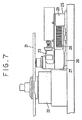
- reference numeral 103 is a spindle motor which rotates an optical disc 101
- 104 is an optical head on which an incidence optical system is disposed in addition to the reflection optical system and others shown in Fig. 2.
- the optical head 104 may be the same as the optical head 23 in Figs. 6 and 7.
- Reflected lights l1 and l2 from the optical disc 101 pass through a quarter-wavelength plate III for two times so that their planes of polarization are rotated by a total of 90 ° , and are incident upon a cylindrical lens 112 through a beam splitter 109.
- the reflected light fl and 2 2 are formed into oblong light bundles by the cylindrical lens 112, and the reflected light l1 is detected by a photodetector 113a while the other reflected light 2 2 is detected by another photodetector 113b.
- a track deviation signal circuit is formed by the photodetectors 113a and 113b, sensor amplifiers 114a and 114b, and a differential amplifier 115.
- the output terminal of the differential amplifier 115 is connected on the one hand to a first junction 116a connected via a lens driving circuit or buffer 117 to a driving coil 106.
- the track deviation signal voltage TS is selectively transferred to the side of the driving coil 106.
- Reference numeral 118 is a linear motor, and the input line of a coarse access signal for moving the optical head is connected via a second junction 116b and a motor driving cirucit (buffer) 119 to the linear motor 118.
- the linear motor 118 is driven by the coarse access signal or the like to move the optical head 104 in a desired direction.
- a voltage comparison circuit 121 which can be set to the predetermined positive and negative reference voltages ⁇ V ref .
- the accuracy of conversion of the track deviation signal voltage TS to the digital quantity B(4) is determined by the voltage values of the reference voltages ⁇ V ref .
- the values of the reference voltage ⁇ V ref are set to those values for which a desired accuracy can be achieved as well as an appropriate conversion sensitivity can be realized.
- the values of the reference voltages ⁇ V ref correspond to the weighting for the least significant bit in the digital quantity B(4).
- the reference voltages ⁇ V ref and the track deviation signal voltage are compared in the voltage comparison circuit 121, and an addition signal C + is output if TS > + Vref and a subtraction signal C- is output if TS ⁇ - Vref.
- Reference numeral 122 is an addition - subtraction data set circuit which sets digital data B(I) for addition and subtraction based on the addition and subtraction signals C + and C- output from the voltage comparison circuit 121.
- the output terminal of the addition-subtraction data set circuit 122 is connected to a full adder 124 whose output terminal is connected via a buffer 125 to a memory 126 for memorizing digital quantities.
- the memory 126 is connected to a latch circuit 127 which latches the data B(3) read from the memory 126 as a digital quantity B(4).
- One of the output terminal of the latch circuit 127 is connected to the full adder 124 while the other terminal is connected to a D/A converter 128.
- the output terminal of the D/A converter 128 is connected to the first junction 116a.
- the data B(3) that corresponds to the eccentricity amount memorized in the memory 126 are composed of eccentricity data for each position on the recording track 102 obtained by subdividing one rotation of the optical disc 101 into desired number of sectors.
- the FG pulses are generated by 76 in number, for example, for one rotation of the optical disc 101.
- Reference numeral 129 is a frequency multiplication circuit which has the function of doubling, for example, the frequency so that an FG pulse is doubled to a 2FG pulse.
- the output terminal of the frequency multiplication circuit 129 is respectively connected to the buffer 125, latch circuit 127, memory 126, and an address counter 131.
- the buffer 125 displays a high impedance when the 2FG pulse is on H level, and when it is on L level, it is in an active state and transfers the calculated data B(2) from the full adder 124 to the memory 126.
- the latch circuit 127 is in an active state when the 2FG pulse is on H level, and reads the stored data B(3) in the memory 126. When the 2FG pulse is on L level, the circuit 127 holds it as a digital quantity B(4).
- the address counter 131 which consists of a loop counter counts the 2FG pulses to control the address of the memory 126, and the eccentricity amount of 152 in number are memorized periodically.
- a data B(3) that corresponds to an interim digital quantity is memorized in the memory 126 in the beginning.
- the track deviation signal circuit there are detected amount of deviation and direction of deviation of the beam spot with respect to each position on the track 102. Then, there is output a track deviation signal voltage TS which has an absolute value proportional to the amount of deviation and has a positive or negative sign in response to the direction of the deviation in the outward or inward direction of the track.
- the track deviation signal voltage TS is compared with the reference voltage ⁇ V ref in the voltage comparison circuit 121. As a result of comparison, if the track deviation signal voltage has a positive sign and its value is greater than +V ref , then an addition signal C + is output, and an addition data is set in the addition-subtraction data set circuit 122.
- the addition and subtraction data B(I) is input to the full adder 124. Since there is input an interim digital quantity from the latch circuit 127 in the other input terminal of the full adder 124, the addition - subtraction data B(I) are respectively added and subtracted, from the interim digital quantity. A new data B(2) obtained by such operation is stored in the memory 126 as data B(3) with the timing when the buffer 125 becomes active.
- the stored data of the memory 126 is rewritten from an interim digital quantity to a corrected data B(3) based on the track deviation signal voltage TS.
- the data B(3) is read by the latch circuit 127 with the timing at which the latch circuit 127 becomes active.
- the digital quantity B(4) held in the latch circuit 127 is converted to an analog voltage by the D/A converter 128 and is applied to the driving coil 106 of the objective 105.
- a series of processes of the detection of the track deviation signal voltage TS by the track deviation signal circuit, addition and subtraction by the full adder 124, rewriting in the memory 126, and so forth are repeated until the absolute value of the track deviation signal voltage TS becomes smaller than the voltage value of the reference voltages ⁇ V ref in the voltage comparison circuit 121. This operation is carried out for each position of the track 102 by the address control using the address counter 131 and others.
- a digital quantity B(4) in response to the eccentricity data B(3) is converted to an analog voltage by the D/A converter 128.
- the analog voltage V dac for eccentricity correction and a precise access signal are applied to the driving coil 106 so that the tracking control of high accuracy can be accomplished even when there is an eccentricity in the optical disc 101.
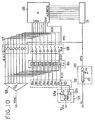
- FIG. 10 is a detailed circuit diagram with the optical head and others omitted
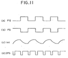
- Fig. ii(a) to Fig. II(d) are timing charts for illustrating the operation of the frequency multiplication circuit 129
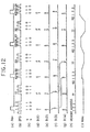
- Fig. 12 is a timing chart for illustrating the operation of the present embodiment
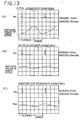
- Fig. 13(A) to Fig. 13(C) are waveform diagrams for showing the eccentricity correction analog voltage and others for illustrating the operation of the above embodiment.
- the circuit configuration will be described by referring to Fig. 10.
- the voltage comparison circuit 121 there are provided two voltage comparators 121a and 121b which are set to reference voltages +Vref and -Vref, respectively.
- the track deviation signal voltage TS is commonly input to the voltage comparators 121a and 121b and is simultaneously compared with the reference voltages ⁇ V ref .
- addition - subtraction data set circuit 122 there is provided only one OR circuit 123, and the output terminals of the voltage comparators 121a and 121b are respectively connected to the two inputs of the OR circuit 123.
- the least significant bit, B 11 of the addition - subtraction data B(1) ⁇ (B 18 , B 17 , ..., B 11 ) is output.
- the other bits B 18 , B 17 , ..., B 12 are directly output from the comparator 121b.
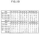
- Table I shows the above relationship in a tabular form.
- the full adder 124 uses ordinary 8-bit system and the addition and subtraction data B(I) output from the addition - subtraction data set circuit 122 is added or subtracted from the digital quantity B(4) input from the latch circuit 127, and the data B(2) obtained by the operation is output to the buffer 125.
- the baffer 125 is driven by a 2FG pulse, and displays a high impedance, an open state, when the 2FG pulse is on H level and is in an active state when the 2FG pulse is on L level.
- Writing of the data B(3) to the memory 126 is controlled by the address counter 131, and the data B(3) is taken-in with address shifted by I each.
- the memory 126 is required to have a capacity of more than 1.2K bits.
- the frequency multiplication circuit 129 which doubles the FG pulses is composed of an integration circuit consisting of an inverter, a resistor, and a capacitor, and an EXOR circuit.
- Figures 11(a) to Fig. II(d) illustrate the doubling operation of the frequency multiplication circuit 129 by which a 2FG pulse in Fig. II(d) is output by taking an exclusive logical sum of an FG pulse in Fig. II(b) and the integration voltage in Fig. II(c).
- Figure 12(a) is a revolution pulse chart that shows the revolving position of the spindle motor 103, and the timing chart is drawn by assuming that 76 periods of FG pulses are generated during I period of the revolution pulse R ev .
- the FG pulses are doubled by the frequency multiplication circuit 129 to generate 2FG pulses shown in Fig. 12(b), and they are counted by the address counter 131 to control the memory address in Fig. 12(h). Therefore, one rotation of the optical disc 101 is equally subdivided into 152 parts, and the eccentricity data at each of the subdivided position is converted to a digital quantity B(3) to be stored in the memory 126.
- the inner circuit of the D/A converter 128 is so constructed as to have the following relationship between the digital quantity B(4) and the analog voltage V dac that is converted.
- V fs means the full scale of the analog voltage V da c.
- a subtraction signal C- I is output from the voltage comparison circuit 121.
- addition and subtraction operation are also carried out with 152 shots of the 2FG pulses as one period.
- Figures 13(A) and 13(B) represent the amount of displacement of the linear motor 118 with respect to the rotation of the optical disc 101 as scale (SCK) signals.
- Figure 13(A) and Fig. 13(B) are waveforms that show the amount of displacement before and after the eccentricity correction, respectively.
- Figure 13(C) is a waveform diagram which shows the analog voltage V dac for eccentricity correction output from the D/A converter 128 as a result of taking-in of the eccentricity data into the memory 126.
- the waveforms of the symbol R ev are the signal waveforms that show the rotation position of the spindle motor 103, and the rotation position of the optical disc 101 can be shown by these signals.
- Fig. 13(A) shows that in the first half of the rotation of the optical disc 101 the linear motor 118 moved to the outer periphery side of the optical disc 101, and in the latter half it moved inward.
- Figure 13(C) shows that when there exists an eccentricity state as above, the eccentricity data is obtained by the memory 126, and the digital quantity B(4) that corresponds to the eccentricity amount is output as an analog voltage for eccentricity correction V d ac by the D/A converter 128.
- the objective 105 moves outward for a negative inclination of the analog voltage V dac and moves inward for a positive inclination, so that the direction of following of the objective 105 also coincides with the direction of motion of the linear motor 118 shown in Fig. 13(A).
- Figure 13(B) shows the amount of displacement of the linear motor 118 when the position of the objective 105 is controlled by the analog voltage for eccentricity correction. From Fig. 13(B) it will be seen that, after eccentricity correction, the amount of displacement of the linear motor 118 is markedly reduced and that the eccentricity correction is being carried out extremely effectively.
- the amount of eccentricity correction is identical if the rotation position is the same so that by the addition of the analog voltage V dac for eccentricity correction as it is to the jump pulse an accurate and stable track jumping becomes possible.
- digital quantity corresponding to the eccentricity quantity of the optical disc is stored in the memory, and the analog voltage for eccentricity correction obtained by D/A converting the digital quantity is added to driving means of the objective, so that tracking control with high accuracy can be achieved even when an eccentricity exists in the optical disc.
- an analog voltage for eccentricity correction output from the D/A converter can be applied as it is to the driving means for the objective along with the jump pulse. Therefore, there is an advantage that track jumping can be carried out accurately and stably while applying the eccentricity correction.
- reference numeral 201 is the input terminal of an input analog voltage Vi n and a differential amplifier 202 outputs the difference voltage ⁇ V in between the input analog voltage Vin and an analog voltage V dac generated from a D/A converter 203 that constitutes a feedback circuit.
- Reference numeral 204 is a voltage comparison circuit, and when the digital quantity B(4) is assumed to be of n bits, there are provided a number 2n of voltage comparators 205 and 206. Further, there are prepared a plurality of positive and negative reference voltages +Vr and -Vr each of which corresponds to the weighting of each bit in the digital quantity B(4). These reference voltages +V r and -V r are set to the respectively corresponding voltage comparators 205 and 206.
- An addition - subtraction data set circuit 207 contains an addition data set section 207a, a subtraction data set section 207b, and an OR circuit 212 which takes a logical sum of the outputs of both data set sections 207a and 207b.
- the output terminal of the OR circuit 212 is connected to a full adder 213 whose output terminal is connected via a buffer 214 to a memory 215 for memorizing digital quantities.
- the memory 215 is connected to a latch circuit 216 for latching the data B(3) read from the memory 215, and the output terminal of the latch circuit 216 is connected to the D/A converter 203.
- the output terminal 217 of the digital quantity B(4) is connected to the output terminal of the latch circuit 216.
- an interim digital quantity initially stored in the memory 215 is read by the latch circuit 216, and an analog voltage voltage V dac proportional to the interim digital quantity is generated.
- V dac an analog voltage voltage
- the difference is taken between the input analog voltage Vi n input from the input terminal 201 and the analog voltage V dac generated in the D/A converter 203, and the difference voltage ⁇ V in given by is output.
- the value of the difference voltage ⁇ V in is proportional to an error in conversion.
- the difference voltage ⁇ V in is simultaneously compared with a plurality of reference voltages + V r and -V r in the voltage comparation circuit 204.
- Ci + is output from the voltage comparator 205.
- an addition data set section 207a of an addition - subtraction data set circuit 207 there is set a binary number for addition data with weighting that corresponds to the absolute value of the difference voltage AVin.
- C 1 - is output from the voltage comparator 206, and a binary number for subtraction data with weighting that corresponds to the absolute value of the difference voltage ⁇ V in is set in the subtraction data set section 207b of the addition - subtraction data set circuit 207.
- the addition data and the subtraction data are logically summed in the OR circuit 212, and the addition subtraction data B(I) are input to the full adder 213.
- An interim digital quantity is input from the latch circuit 216 to the other input terminal of the full adder 213, so that the addition - subtraction data B(I) is added and subtracted from the interim digital quantity.
- the new digital quantity B(2) obtained as the result of the above operation is stored in the memory 215 via the buffer 214.
- the stored data in the memory 215 is rewritten from the interim digital quantity to a digital quantity B(3) corrected based on the difference voltage ⁇ V in .
- An A/D converter of 4 bits is used in the following embodiment.
- a sample hold circuit 218 is connected between an input terminal 201 and a differential amplifier 202.
- the sample hold circuit 218 is the one for temporarily holding an input analog voltage Vin, and is used to avoid an influence on an output digital quantity B(4) due to variations in the input analog voltage Vin during A/D conversion.
- a voltage comparison circuit 204 there are provided side by side a number 8, which corresponds to twice as many the number of bits, of voltage comparators 205a to 205d and 206a to 206d. Further, a voltage of +16V r is divided by a voltage dividing circuit formed by connecting five resistors with resistances R, 2R, 4R, and 8R in series to generate positive reference voltages with values that correspond to the weightings for the bits, namely, V r , 2V r , 4V r , and 8V r set to the voltage comparators 205a, 205b, 205c, and 205d, respectively.
- a voltage of - 16Vr is divided by another voltage dividing circuit formed by connecting five resistors similar to the above, to generate negative reference voltages with absolute values that correspond to the weightings for the bits, namely, -V r , -2V r , -4V r , and -8Vr set to the voltage comparators 206a, 206b, 206c, and 206d, respectively.
- an addition data set section 207a of an addition - subtraction data set circuit 207 there are arranged side by side three AND circuits 208a, 208b, and 208c, and one of the two inputs of the AND circuit 208a is directly connected to the voltage comparator 205a and the other input is connected via an inverter 209a to the voltage comparator 205b.
- the situation is similar to the case of the AND circuit 208a. Namely, for the AND circuit 208b, the voltage comparator 205b is connected directly, and the voltage comparator 205c is connected via an inverter 209b.
- the voltage comparator 205c is ocnnected directly, and the voltage comparator 205d is connected via an inverter 209c.
- the conditions for connection are similar to the above, with three AND circuits 210a to 210c and three inverters 211a to 211c arranged side by side.
- a main portion of the 4-bit D/A converter 203 consists of a ladder type resistor circuit formed by five resistors that have resistance of 2R and three resistors that have resistance of R, and an inverting amplifier formed by an operational amplifier 221 and a resistor with resistance (16/5)R.
- sample hold circuit 218, differential amplifier 202, voltage comparison circuit 204, and the analog circuit portion including the D/A converter 203 mentioned in connection with Fig. 16 will be described.
- the sample hold circuit 218 consists of two operational amplifiers 223 and 224, and a switch 225 and a capacitor 226 connected between the operational amplifiers 223 and 224.
- the switch 225 is driven by (I/4) CK obtained by frequency-dividing the clock CK into four, and the input analog voltage Vi n is held in the capacitor 226.
- the differential amplifier 202 is of the ordinary type that consists of an operational amplifier 202a.
- transistors 227a and 227b are connected to the output terminals of the voltage comparators 205a to 205d and 206a to 206d, although these are omitted in Fig. 15.
- an analog-logic interface circuit constructed by two diodes D 1 and D 2 and three resistors Ri, R 2 , and R 3 , is connected to the output terminal of each of the voltage comparators.
- the logic circuit portion that follows the addition - subtraction data set circuit 207 is operated, for example, by a power supply voltage of +5V, so that the ranges of operating voltage for both circuit portions are ordinarily different from each other. For this reason, an interface circuit is used in order to supply signals with normal logical amplitude from the analog circuit portion to the logic circuit portion.
- V ee is the emitter voltage of the transistor 227a and V cesat is the saturation voltage, and the voltage V 1 becomes equal to V ee if Vcesat can be neglected.
- V 2 and V 3 are given by where V f1 and V f2 are the forward voltage drops of the diodes D i and D 2 , respectively.
- addition data A 1 to A4 are output to set the addition - subtraction data B(I) that correspond to each bit in the following way.
- addition data A 1 to A4 have the following relations with the outputs C t to C 4 of the voltage comparators 205a to 205d.
- subtraction data S 1 to S 4 are output to set an addition - subtraction data B(I) for each bit as in the following.
- (0001) need be subtracted in the full adder 213 from the digital quantity B(4) so that (IIII) is set for the addition - subtraction data B(I).
- the set value (IIII) corresponds to adding I to the least significant bit to (IIIO) which is the inversion of each bit of (0001).
- the subtraction data S 1 to S 4 have the following relations with the outputs C 1 - to C 4 - of the voltage comparators 206a to 206d.
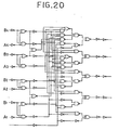
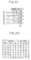
- the 4-bit full adder 213 use is made of a disclosed apparatus so that detailed description about its internal configuration and others will be omitted by simply giving its logical diagram in Fig. 20, block diagram in Fig. 21, and the truth table between inputs and outputs.
- the digital quantity B(4) (B 44 , B 43 , B 42 , B 41 ) stored in the memory 215 is (0000).
- the addition - subtraction data B(I) (B 14 , B 13 , B 12 , B 11 ) is set to (1000) based on the outputs C 4 to C 1 .
- the digital quantity B(14) memorized in the memory 215 becomes (1000). Because of this, the analog voltage V dac output from the D/A converter 203 in proportion to the digital quantity B(4) is changed to 8V.
- This data B(2) becomes a data B(3) via the buffer 214, and is written in the memory 215.
- the data B(3) (IIIO) is stored in the memory 215.
- the data B(2) becomes a data B(3) via the buffer 214 and is written in the memory 215.
- the output of the voltage comparison circuit 214 becomes (C 4 -, Cs-, C 2 -, C 1- ) _ (0011)
- the data B(3) (0001) is written in the memory 215.
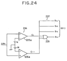
- Fig. 24 shows a modification of the portions of the voltage comparison circuit and the addition and subtraction data set circuit in the 4-bit A/D converter.
- a voltage comparison circuit 234 there are arranged in a voltage comparison circuit 234 only two voltage comparators 205a and 206a for setting reference voltages +V r and -Vr, respectively.
- one OR circuit 229 alone is arranged, and two input terminals of the OR circuit 229 are connected to the output terminals of the voltage comparators 205a and 206a respectively.
- the least significant bit B 11 in the addition subtraction data B(I) (B 14 , B 13 , B 12 , B 11 ) is output from the OR circuit 229.
- the other bits B 14 , B 13 , and B 12 are directly output from the voltage comparator 206a.
- the addition - subtraction data B(I) in the above is added - subtracted in the full adder 213 from the digital quantity B(4) read from the memory 215, the digital quantity B(4) is successively corrected in minimum bit unit, and an A/D converted digital quantity B(4) is output from the output terminal 217.
- the configuration of the voltage comparison circuit 234 and the addition - subtraction data set circuit 237 can be made extremely simple.
- A/D conversion is carried out in terms of the correction made in the least significant bit unit of the digital quantity B(4) read from the memory so that its conversion time is somewhat longer compared with the voltage comparison circuit 204 and the addition - subtraction data set circuit 207 shown in Fig. 15.
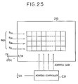
- Fig. 25 shows a modification of the memory portion Although in the memory 215 shown in Fig. 15 the address for storing digital quantity is fixed, in the present modification it is arranged that address control can be carried out by providing an address controller 231.
- the address controller 231 is driven by (I/4) CK obtained by dividing the frequency of the clock CK into four, and an address data is output to control the address of the memory 215.
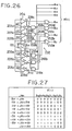
- Figs. 26 and 27 show an embodiment of an 8-bit A/D converter according to the present invention.
- a voltage comparison circuit 204 has the same system as for the 4-bit converter shown in Fig. 15.
- the addition - subtraction data B'(I) B 18 to B 11 shown in Fig. 27 are added or subtracted in the full adder 213, from the digital quantity B'(4) read from the memory 215 to correct the digital quantity B'(4).
- addition and subtraction are carried out with the four bits (00001000) of the addition - subtraction data B'(I) as a unit.
- the voltage comparison circuit there are set a plurality of positive and negative reference voltages whose values are related to the weightings for the bits in the digital quantity.
- the difference voltage between the input analog voltage and the analog voltage generated in the D/A converter is simultaneously compared with the plurality of reference voltages in the voltage comparison circuit.
- a binary number with weighting that corresponds to the absolute value of the difference voltage is added to or subtracted in the full adder from the digital quantity read from the memory.
- the new digital quantity obtained as the result of the above operation is stored in the memory, and the above process is repeated until the absolute value of the difference voltage becomes smaller than the reference voltage corresponding to the weighting for the least significant bit.
Landscapes
- Optical Recording Or Reproduction (AREA)
- Moving Of The Head For Recording And Reproducing By Optical Means (AREA)
Description
- The present invention relates to an optical disc apparatus which carries out recording or reproducing of information by the tracking of an optical head with respect to a rotating optical disc, and more particularly to an eccentricity correction means of the optical disc.
- In general, in an optical disc apparatus of the above kind, an optical disc has concentric circular or spiral recording tracks as information recording medium, and the recording or reproducing of information for the recording track of the optical disc is carried out by linearly moving the recording head in the radial direction of the optical disc while rotating the disc.
- In such an optical disc apparatus, the optical head has to precisely follow the recording tracks of the rotating disc. For this reason, tracking control is ordinarily carried out by using a tracking servo system.
- Now, in the optical disc apparatus of the above description, when the optical head is moved from an arbitrary recording track which is in rotation to another recording track, tracking is interrupted for a while to move the optical head for a distance which corresponds to the separation between the present and desired tracks, and tracking is resumed. However, the recording tracks themselves of the optical disc are in general not necessarily concentric with respect to the center of the rotation shaft of the motor that drives to rotate the optical disc, and are often eccentric. Because of this, when tracking is interrupted once, the relative position of the optical head with respect to the recording track has a dispersion that corresponds to the eccentricity amount so that when tracking is resumed after the head has been moved, it leads to a drawback that accuracy tends to be lowered by the deviation corresponding to the dispersion. This results in a difficulty in reducing the time for positioning the optical head to the desired track.
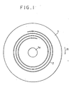
- Further, in the optical disc I. as shown in Fig. I, there is given in advance a spiral pre-groove 2 for tracking on the surface of the substrate, in order to facilitate recording and reproducing. Since the recording track is provided in the pre-groove 2, the portion identical to that of the pre-groove 2 is referred to simply as the track hereinafter.
- In Fig. for facilitating the understanding, the track pitch is drawn schematically with wide separation. However, the real track is formed with a considerably small pitch of the order of µm.
- The optical disc I is placed on a spindle motor, as will be described later, to be rotated in the direction of the arrow R of Fig. I. Accompanying the rotation, the beam spot (laser spot) of the optical beam projected from the optical head is traced on the
track 2. The beam spot is shifted totrack 2 by one track outward for each one rotation of the optical disc I. - Recording of information is made by the change in reflectivity generated by the phase transition or the like in a thin film layer in the track portion of the disc, through irradiation of the beam spot whose intensity is modulated by an information signal.
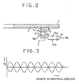
- Fig. 2 shows a track control device for causing the
optical head 4 to follow thetrack 2 in recording and reproducing information from the optical disc I as in the above. In Fig. 2, a light source is omitted to simplify the track control device. - In the
optical head 4,reference numeral 5 is an objective lens which lets the beam spot of the light beam to be projected on the optical disc I, 6 is a driving coil for controlling the position of theobjective lens 5 in the radial direction of the optical disc I, 13a and 13b are photodetector for detecting the intensities of reflected lights BI and 12, respectively,photodetector 13a being connected to the negative input terminal of a differential amplifier 15a via asensor amplifier 14a whilephotodetector 13b is connected to the positive input terminal of thedifferential amplifier 15 via anothersensor amplifier 14b. - It should be noted that there is provided an optical system for incidence from the laser diode as will be described later. However, for the sake of convenience of explanation the incidence optical system is omitted in Fig. 2 and the configuration of the reflection optical system is illustrated mainly.
- If the beam spot is projected correctly on the pre-groove 2 as shown in the figure and the track following is carried out precisely, then the intensities of both reflected
lights 21 and e2 become equal and the track difference signal voltage TS output from thedifferential amplifier 15 becomes zero. - If the beam spot is shifted toward the center of the optical disc I as shown by the arrow in Fig. 2, the
reflected light 21 is reflected from the surface portion of the disc (the area outside the pre-groove 2) with larger intensity, giving larger detected value to thephotodetector 13a, and causes thedifferential amplifier 15 to output a negative track deviation signal voltage - TS. - If the beam spot is shifted in the direction opposite to the arrow in Fig. 2, the
reflected light 12 has a larger intensity opposite to the above, and there is output a positive track deviation signal voltage + TS from the differential amplifier. - The track control is carried out by applying the positive and negative track deviation signal voltages ± TS to the
driving coil 6 and controls the position of theobjective 5 to have the track difference signal voltage TS to be zero. By applying tracking servo so as to make the track deviation signal voltage TS zero, the beam spot follows thetrack 2 to carry out the correct recording and reproducing. - The optical disc apparatus can carry out the operation of repeatedly reproducing an identical track of one turn, the so-called track-on mode, in addition to the ordinary operation of recording and reproducing as in the above.
- The track-on made operation can be realized by applying a jump pulse to the
driving coil 6 at the timing when the optical disc I completed one rotation, to cause the beam spot to jump to the adjacent previous track. - In carrying out the track jump, the loop of the tracking servo is open.
- The solid waveform in Fig. 3 is the output waveform of the track deviation signal voltage TS when the track jump is carried out by passing a current in the driving coil in the direction of the arrow in Fig. 2, and the broken-line waveform is the output waveform for the track deviation signal voltage TS when the track jump is carried out in the opposite direction.
- The track deviation signal voltage TS is output as a waveform for one cycle every time when the
optical head 2 traverses the pre-groove 2. Therefore, the number of waves in the track deviation signal voltage TS corresponds to the number of tracks jumped. - Now, when the optical disc I is mounted on the spindle motor, it is usual that the central point Cpl of the optical disc I and the center Cp2 of the rotation shaft of the spindle motor do not coincide perfectly, producing eccentricity for the optical disc I, due to the accuracy of the center hole of the optical disc I, errors generated in chucking the disc to the spindle moter, and so on.
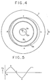
- To illustrate the situation schematically, let us approximate the track by
concentric circles 2a and 2b. If one assumes that the optical disc I is rotated in the direction of arrow R in Fig. 4 and the beam spot from theoptical head 4 is projected on a fixed position, then the locus of the beam spot will be a dotted circle which has the rotation center Cp2 of the spindle motor as the center. Thus, for the track 2a, the beam spot coincides with the track 2a at points a and c, but deviates by the amount of eccentricity at points b and d, where it is shifted to the outside of the track 2a at point b while it is shifted to the inside of the track 2a at point d. - Fig. 5 shows the waveform of the track difference signal voltage TS on which each of the points a, b, c and d is indicated.
- If the tracking servo is in effect, the track deviation signal voltage TS is applied to the
driving coil 6, and the beam spot is corrected to follow thetrack 2 so as to be moved to the inside at point b and to the outside at point d. - As in the above, even if the optical disc I is placed on the spindle motor with eccentricity relative to the rotating center of the motor, when the tracking servo is turned on, the beam spot can be made to follow the
track 2 correctly. However, when a track jump is carried out, the loop of the tracking servo is brought to an open state. Because of this, when the beam spot which has been following the track 2a is jumped, for example, to thetrack 2b, the beam spot deviates from the track 2a in the vicinities of the points b and d. Therefore, there occurs a problem in making a jump from the track 2a to thetrack 2b in that the track jumping is unstable by the variations in the jumping distance in the vicinities of the point b and the point d. - Now, a successive comparison type A/D converter is known as A/D converter used in the prior art optical disc apparatus which can carry out high precision A/D conversion.
- The A/D converter has a voltage comparison circuit, a successive comparison register, a D/A converter that constitutes the feedback circuit, a clock oscillator which carries out the overall control, and so on.
- With this converter, a digital quantity which corresponds to the input analog voltage is arranged to be output by the following way. Namely, starting with the least significant bit of the successive comparison register, a converted voltage that corresponds to each one bit is arranged to be output from the D/A converter to compare the converted voltage with the input analog voltage in the voltage comparison circuit. If these two voltages do not coincide, the same procedure is successively repeated for each bit, until agreement is obtained.
- However, in the successive comparison type A/D converter as in the above, an analog voltage is converted to a digital quantity by the successive comparison of the smallest bit unit. Accordingly, there was a problem in that it is unsatisfactory because of the lack of high speed property of the operation due to a relatively long time required before obtaining the digital quantity.
- On the other hand, a parallel comparison type A/D converter is known as another existing A/D converter which can carry out A/D conversion at high speed.
- The A/D converter comparises a resistor ladder circuit which generates (2n-1) reference voltages by subdividing a given voltage into 2n equal parts when the digital quantity to be output has n bits, (2r-l) voltage comparators to each of their reference terminals for setting each of the reference voltages generated in the resistor ladder circuit, and a decoder which transmits the outputs of the voltage comparators as an n-bit digital quantity after binary coding conversion.
- With this construction, an input analog voltage is input parallel to the input terminals of all of the voltage comparators and compared at once with all of the reference voltages, to output from the decoder a digital quantity that corresponds to the input analog voltage.
- However, in the parallel comparison type A/D converter described above, there are required a large number, (2rL-1), of voltage comparators for the digital quantity of n bits. Because of this, factors for accuracy deterioration such as the dispersion in the threshold voltage, input bias current, input offset voltage, and delay time, for each of the voltage comparators, and the relative accuracy of the resistor ladder circuit, are augmented, giving rise to a difficulty in achieving a high accuracy A/D conversion.
- EP-
A 0 076 347 describes an optical playback machine which plays back data recorded on an optical record in track segments, employs a track intercept apparatus to transversely deflect a scanning light beam during each scan to accurately intercept each selected track segment despite record or optical misalignment. A track intercept control circuit includes storage means for storage of variable values of track alignment data, adjust means for producing an adjustment signal from the stored data and timing means controlling gating circuitry for applying the adjustment signal to a light beam deflection means at the proper point in each scan. - EP-
A 0 162 702 describes a tracking control arrangement for use in an optical disc player comprising a photodetector for receiving a light beam reflected at an optical disc on which an information signal is recorded in a record track, signal generating circuit for generating a reproduced information signal and a tracking error signal from the output of the photodetector, a modifier for modifying the tracking error signal in response to variations in the total quantity of light of the light beam received by the photodetector, driving means for driving an optical device to maintain the light beam in a proper tracking relation to the record track in response to the modified tracking error signal, a detector for detecting a variation in the reproduced information signal resulting from the condition in which the light beam reflected at a blank area in the record track is received by the photodetector and a gain controller for varying the gain of transmission of the modified tracking error signal from the modifier to the driving means in response to a predetermined detection output of the detector. - An object of the present invention, in view of the above circumstances, is to provide an optical disc appratus which enables the optical head to precisely follow the recording track on the optical disc by minimizing the amount of eccentricity between the optical head and the optical disc.
- Another object of the present invention is to provide an eccentricity correction device in the optical disc apparatus which enables a precise track jump.
- Still another object of the present invention is to provide an A/D converter which can carry out high accuracy A/D conversion at high speed.
- In order to achieve the above objects, an optical disc apparatus is provided including, optical means for recording or reproducing information on the recording track of an optical disc; means for detecting at least deviation amount of beam spot projected from said optical means on the recording track of the optical disc and generating a track deviation signal based on the deviation amount; means for comparing the track deviation signal with a reference signal; and means for converting the digital quantity read from said memory means to an analog signal for driving said optical means, characterized by means for memorizing a first digital quantity; and means for calculating a second digital quantity based on the digital output of the comparison means and the first digital quantity from the memory means and transferring the second digital quantity to the memory means and repeating said calculation of the second digital quantity until the voltage of the track deviation signal become smaller than the voltage of said reference signal.
- The optical disc apparatus in the present invention reads via an A/D converter, the position deviation of tracking output from an optical head, prior to the actual operation of recording or reproducing and stores it as eccentricity correction data after giving a predetermined data processing. In an actual recording or reproducing operation, the eccentricity correction data that has been stored is transferred to a D/A converter and the amount of eccentricity between the optical head and the optical disc is minimized by giving the output of the D/A converter to a tracking control means.
- Moreover, in the present invention, in the voltage comparison circuit, there are set a plurality of positive and negative reference voltages related to the weighting of each bit, and by generating an analog voltage proportional to an interim digital quantity stored in the memory in the D/A converter, the difference voltage between the input analog voltage and the generated analog voltage is simultaneously compared with the plurality of reference voltages in the voltage comparison circuit. Based on the output from the voltage comparison circuit, a binary number weighted corresponding to the absolute value of the difference voltage, in response to the positive or negative sign of the difference voltage, is added or subtracted by the adder from the digital quantity read from the memory. The new digital quantity obtained in this way as the result of the arithmetic operation is stored in the memory, and the above operation is repeated until the absolute value of the difference voltage becomes smaller than the reference voltage that corresponds to the weighting for the least significant bit. In this manner, high accuracy A/D conversion is arranged to be accomplished at high speed.
- These and other objects, features and advantages of the present invention will be more apprent from the following description of the preferred embodiments taken in conjunction with the accompanying drawings in which:
- Fig. I is a plan view showing an optical disc;
- Fig. 2 is a side view with partially sectional view which shows the prior-art optical disc;
- Fig. 3 is a waveform diagram that shows the output waveforms of the track deviation signal voltage in the above optical disc apparatus;
- Fig. 4 is a plan view showing the eccentricity situation of the prior art optical disc apparatus in the above;
- Fig. 5 is a waveform diagram which shows the output waveform of the track deviation signal voltage in the eccentricity state;
- Fig. 6 is an overall block diagram of an optical disc apparatus to which the present invention can be applied;
- Fig. 7 is a side view showing the linear motor portion;
- Fig. 8 is a diagram showing an optical disc which is subdivided into 256 sectors in the circumferential direction;
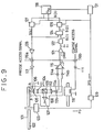
- Fig. 9 is a block diagram showing the basic configuration of the eccentricity correction device in the optical disc apparatus in accordance with the present invention;
- Fig. 10 is a circuit diagram for an embodiment of the present invention, with the optical head and other portions omitted;
- Fig. II is a timing chart illustrating the operation of the frequency multiplying circuit in the embodiment;
- Fig. 12 is a timing chart illustrating the operation of the embodiment;
- Fig. 13 is a waveform diagram showing the waveform of the analog voltage for eccentricity correction and other waveforms;
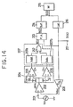
- Fig. 14 is a block diagram showing the basic configuration of the weighted operation type A/D converter in accordance with the present invention;
- Fig. 15 is a block diagram showing the overall configuration of the weighted operation type A/D converter;
- Fig. 16 is a circuit diagram for the important part of the D/A converter;
- Fig. 17 is a circuit diagram for the analog circuit portion in the first half thereof;
- Fig. 18 is a circuit diagram for the portions of the voltage comparison circuit and the addition-subtraction data set circuit;
- Fig. 19 is a diagram showing the addition and subtraction data set in the addition-subtraction data set circuit;
- Fig. 20 is a logic diagram of the full adder;
- Fig. 21 is a block diagram for the full adder;
- Fig. 22 is the truth table for the full adder;
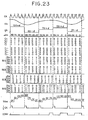
- Fig. 23 is a timing chart for illustrating the operation of the full adder;
- Fig. 24 is a circuit diagram showing a modification of the voltage comparison circuit and the addition-subtraction data set circuit;
- Fig. 25 is a block diagram showing a modification of the memory portion;
- Fig. 26 is a circuit diagram showing the important part of another embodiment of the present invention; and
- Fig. 27 is a diagram showing the ralationship between the difference voltage and the addition-subtraction data for the embodiment in Fig. 26.
- An optical disc apparatus to which the present invention can be applied will be described with reference to the drawings.
- In Fig. 6, 21 is an optical disc, 22 is a driving motor for rotating the
optical disc optical disc 21 has a concentric circular orspiral recording track 300, as shown in Fig. 8, and one rotation of the optical disc is subdivided into 256 sectors of "0 to 255" for data memory. Themotor 22 is driven by amotor control circuit 24. - A laser oscillator 31 is used as a laser beam light generating means, and an objective 35 concentrates beam light on the
optical disc 21 and positions the beam light on the recording track. A vertical driving coil 36 moves the objective 35 in the vertical direction, the direction of the optical axis, and a radial driving coil 37 moves as a tracking means the objective 35 in the radial direction, the direction orthogonal to the optical axis of theoptical disc 21.Split beam detectors optical disc 21. - The laser oscillator 31 generates laser beam light by oscillation driven by a driving
circuit 44. In this case, when information is recorded on the recording track of theoptical disc 21, the laser oscillator 31 generates laser beam light whose intensity is modulated in response to the information to be recorded, and when information is reproduced from the recording track, the laser oscillator 31 generates laser beam light which has a constant intensity. The beam light from the laser oscillator 31 is led, after made into parallel beams of light by a collimator lens 32, to a polarizedlight beam splitter 33 where it is reflected on the side of theoptical disc 21. The reflected beam light is led to the objective 35 through a quarter-wavelength plate 34, and is irradiated on the recording track of theoptical disc 21 after being made into a spot- like beam light by the focusing of the objective 35. The reflected light from theoptical disc 21 by this light irradiation, is led through the objective 35, the quarter-wavelength plate 34, and the polarizedlight beam splitter 33 to ahalf prism 38 where it is split into two systems of light. One of the split reflected lights is focused through acondenser 39 and aknife edge 40 on the light-receiving surface of thelight detector 41 where it is photoelectrically converted. Each of the output signals of thelight detector 41 is used for the focusing control. The other of the slit reflected lights is focused through acondenser 42 on the light-receiving surface of thelight detector 43 where it is photoelectrically converted. Each of the output signals of thelight detector 43 is used for tracking control and for reading of recorded information as described later. - Each of the output signals of the
light detector 41 is supplied to adifferential amplifier 45 from whose output it is arranged to be able to obtain a focus deviation signal of the beam light on theoptical disc 21. The focus deviation signal output from thedifferential amplifier 45 is supplied to a focusingcontrol circuit 46. In response to the input focus deviation signal, the focusingcontrol circuit 46 controls the driving coil 36 for the vertical direction, and carries out focusing control by driving the objective 35 in the vertical direction so as to position the beam light that irradiates theoptical disc 21 to be correctly focused all the time. - Each of the output signals of the
light detector 43 is supplied respectively to adifferential amplifier 47 whose output is arranged to give a tracking position deviation signal. The tracking position deviation signal output of thedifferential amplifier 47 is supplied respectively to atracking control circuit 48 as a tracking control means and an A/D converter 49. In response to the input tracking position deviation signal, thetracking control circuit 48 controls the driving coil for radial direction 37, and carries out tracking control so as to position the beam light to be on the recording track all the time and the beam light precisely follows the recording track, by driving the objective 35 in the radial direction of theoptical disc 21. It is to be noted that in the state when the tracking is in progress, servo mechanism is on for not only the objective 35 but also the linearmotor control circuit 30 to determine the positioning of the beam light by the use of the objective 35 and thelinear motor 25. The A/D converter 49 outputs the input tracking position deviation signal to adata bus 50 by converting it into a digital signal. - Further, each output signal of the
light detector 43 is supplied respectively to avideo circuit 51. Thevideo circuit 51 generates a reproduced signal of recorded information, namely, a video signal reflecting bits within the recording track, by adding each output signal of thelight detector 43, and outputs the video signal by binary coding it to thedata bus 50 as reading information. - Connected to the
data bus 50 are the drivingcircuit 44, the linearmotor control circuit 30, and themotor control circuit 24. Also connected to thedata bus 50 are asector counter 52, a CPU which governs theoverall control 53, aROM 54 storing the operating program of the CPU and the like, aRAM 55 as a memory means for memorizing the eccentricity correction data, and a D/A converter 56. Thesector counter 52 is actuated by the 256 sector pulses per rotation of theoptical disc 21 generated from themotor control circuit 24. A counter simply counts "from 0 to 255," and the counted value is output to thedata bus 50 as well as is supplied to one of the input terminals of theselector 57 as an address signal of theRAM 55. Theselector 57 operates switching by a hold acknowledge signal from theCPU 53, and its output terminal is connected to theROM 54 and theRAM 55 via anaddress bus 58. When a hold pulse is input from a holdpulse generation circuit 59, theCPU 53 becomes a held state, and generates a hold acknowledge signal which indicates that it is being held. The hold acknowledge signal is supplied to theselector 57,RAM 55, D/A converter 56, and holdpulse generation circuit 59. The D/A converter 56 converts the data transferred from theRAM 55 to an analog signal, and supplies the converted output to thetracking control circuit 48 and the linearmotor control circuit 30 as bias. The holdpulse generation circuit 59 is a latch circuit which is set by the rising of a sector pulse generated from themotor control circuit 24 and reset by a hold acknowledge signal, and generates a hold pulse which becomes high level and low level in response to the set and reset, respectively. - In the apparatus having the construction mentioned above, first, a course access for moving the beam spot is gained by reading position information recorded in advance in the recording track of the
optical disc 21 and moving theoptical head 23 by thelinear motor 25 to the vicinity of the target recording track. Then, by carrying out a precision access by using the objective 35, it becomes possible to move the beam light to the desired recording track. These operations are carried out by the control of theCPU 53. Since such an access operation is already well known, further explanation will be omitted. - Next, eccentricity correction of the tracking will be described. First prior to an actual recording or reproducing operation, the
optical disc 21 is rotated by themotor 22, and let the focusing operation take place at an arbitrary position on theoptical disc 21. In this state, for each sector indicated by the counted value of thesector counter 52, theCPU 53 reads, via thedata bus 50, the output of the A/D counter 49 carrying out A/D conversion of the tracking position deviation signal obtained from the output of thedifferential amplifier 47. After giving a predetermined data processing to the output of the A/D converter 49, it is stored in theRAM 55 as eccentricity correction data. Here, the predetermined data. processing carried out in theCPU 53 consists, for example, of storing temporarily the data read corresponding to a plural number of rotations of theoptical disc 21, and reading the data and taking average for each sector and storing the result again in theRAM 55 as eccentricity correction data. In doing so, a plurality of eccentricity correction data are prepared corresponding to the positions of theoptical head 23 for the radial direction of theoptical disc 21, for instance, the inner periphery position, an intermediate position, and the outer periphery position. - When the eccentricity correction data is obtained in this manner, in the actual operation of recording and reproducing of information, eccentricity correction is carried out by successively reading the eccentricity correction data corresponding to each sector from the
RAM 55. Namely, the eccentricity correction is started by the actuation of the holdpulse generation circuit 59. The holdpulse generation circuit 59 generates a hold pulse every time when the sector is switched, and hold theCPU 53 by the hold pulse. TheCPU 53 generates a hold acknowledge signal every time when it is held by a hold pulse. By switching theselector 57 by a hold acknowledge signal, the output of theaddress bus 58 is switched from theCPU 53 to thesector counter 52. At the same time, by enabling the output of theRAM 55 as well as the input of the D/A converter 56, by the hold acknowledge signal, data in theRAM 55 is transferred to the D/A converter 56 while theCPU 53 is being held. This operation is repeated every time when the sector is switched. The address of theRAM 55 is designated by thesector counter 52, and by this relationship a sector and an address are in correspondence all the time. In this case, eccentricity correction data prepared in a plural number in theRAM 55 corresponding to the positions of theoptical head 23 for theoptical disc 21, are switched and transferred. In addition, considering the response delay of thetracking control circuit 48, control is carried out in this case so as to transfer the eccentricity correction data to the D/A connector 56, by shifting the timing to one earlier than that for the target sector. The output of the D/A converter 56 is sent to thetracking control circuit 48, and is given as a bias for the driving signal of the driving coil for radial direction 37. In this way, it becomes possible to sharply reduce the apparent eccentricity amount. - With the eccentricity correction as above, it is possible to reduce the apparent eccentricity amount between the
optical head 23 and theoptical disc 21, and the beam light from theoptical head 23 can be made to follow the recording track precisely. In addition, tracking also becomes easy in moving theoptical head 23 to an arbitrary recording track. In particular, by averaging the data for a plural number of rotations of theoptical disc 21, it becomes possible to avoid reading errors of the A/D converter 49, or the like. Moreover, by switching the eccentricity correction data in response to the position of theoptical head 23 to theoptical disc 21, it is possible for theoptical head 23 to precisely follow the recording track even for a delicate difference in eccentricity of the position in the radial direction of theoptical disc 21. Further, eccentricity correction data are output by considering the response delay in thetracking control circuit 48 so that it is possible to precisely follow the actual eccedntricity in theoptical disc 21. - It is to be noted that the reading of the tracking position deviation signal and the execution of a predetermined data processing by the
CPU 53 are not limited to the embodiments given above. Thus, for example, it may be arranged to read the output of the A/D converter 49 for a plural of times for each sector, memorizing these data temporarily in theRAM 55, and take average of a plurality of data by reading the data for each sector, to store the result in theRAM 55 as the eccentricity correction data. By taking average of a plurality of data within one sector, it is possible to obtain a value for each sector close to the true eccentricity amount, and to improve the data linkage with the preceding and succeeding sectors. - Moreover, a predetermined data processing carried out by the
CPU 53 is not limited to those of the embodiments in the foregoing. For instance, it may be arranged to temporarily store in theRAM 55 the data for one rotation of theoptical disc 21, and read these data and by removing the bias component due to inclination and the like of theoptical head 23 from the data, to store them in theRAM 55 as the eccentricity correction data. In this manner, by removing the bias component due to inclination or the like of theoptical head 23, it is possible to follow the eccentricity of theoptical disc 21 at the most stable position of theoptical head 23. - As described in detail in the foregoing, according to the present invention, it is possible to provide an optical disc apparatus which can reduce the apparent eccentricity amount between the optical head and the optical disc, and permit the optical head to precisely follow the recording track on the optical disc.
- Next, the principle of the eccentricity correction device in the optical disc apparatus in accordance with an embodiment of the present invention will be described.
- In Fig. 9,
reference numeral 103 is a spindle motor which rotates anoptical disc 101, and 104 is an optical head on which an incidence optical system is disposed in addition to the reflection optical system and others shown in Fig. 2. The optical head 104 may be the same as theoptical head 23 in Figs. 6 and 7. - Reflected lights ℓ1 and ℓ2 from the
optical disc 101 pass through a quarter-wavelength plate III for two times so that their planes of polarization are rotated by a total of 90°, and are incident upon acylindrical lens 112 through abeam splitter 109. - The reflected light fl and 22 are formed into oblong light bundles by the
cylindrical lens 112, and the reflected light ℓ1 is detected by aphotodetector 113a while the other reflected light 22 is detected by anotherphotodetector 113b. - A track deviation signal circuit is formed by the
photodetectors sensor amplifiers differential amplifier 115. The output terminal of thedifferential amplifier 115 is connected on the one hand to afirst junction 116a connected via a lens driving circuit or buffer 117 to a drivingcoil 106. - Through the
first junction 116a, the track deviation signal voltage TS, a precise access signal, and an analog voltage from a D/A converter that will be described later, are selectively transferred to the side of the drivingcoil 106. - Reference numeral 118 is a linear motor, and the input line of a coarse access signal for moving the optical head is connected via a
second junction 116b and a motor driving cirucit (buffer) 119 to the linear motor 118. When in such a case the eccentricity amount of theoptical disc 101 is large, where the beam spot has to be moved for a larger distance, the linear motor 118 is driven by the coarse access signal or the like to move the optical head 104 in a desired direction. - Further, between the output terminal of the
differential amplifier 115 and thejunction 116a there are connected various devices having the function of converting the track deviation signal voltage TS to a digital quantity B(4). - Namely, to the output terminal of the
differential amplifier 115, there is connected avoltage comparison circuit 121 which can be set to the predetermined positive and negative reference voltages ±Vref. The accuracy of conversion of the track deviation signal voltage TS to the digital quantity B(4) is determined by the voltage values of the reference voltages ±Vref. For this reason, the values of the reference voltage ±Vref are set to those values for which a desired accuracy can be achieved as well as an appropriate conversion sensitivity can be realized. Here, the values of the reference voltages ±Vref correspond to the weighting for the least significant bit in the digital quantity B(4). - The reference voltages ±Vref and the track deviation signal voltage are compared in the
voltage comparison circuit 121, and an addition signal C+ is output if TS > + Vref and a subtraction signal C- is output if TS < - Vref. -
Reference numeral 122 is an addition - subtraction data set circuit which sets digital data B(I) for addition and subtraction based on the addition and subtraction signals C+ and C- output from thevoltage comparison circuit 121. - The output terminal of the addition-subtraction
data set circuit 122 is connected to afull adder 124 whose output terminal is connected via abuffer 125 to amemory 126 for memorizing digital quantities. Thememory 126 is connected to alatch circuit 127 which latches the data B(3) read from thememory 126 as a digital quantity B(4). One of the output terminal of thelatch circuit 127 is connected to thefull adder 124 while the other terminal is connected to a D/A converter 128. - The output terminal of the D/
A converter 128 is connected to thefirst junction 116a. - The data B(3) that corresponds to the eccentricity amount memorized in the
memory 126 are composed of eccentricity data for each position on therecording track 102 obtained by subdividing one rotation of theoptical disc 101 into desired number of sectors. As a means for obtaining such a digital quantity B(4), use is made of a frequency generator (FG) pulse generated from an unillustrated frequency generator attached to aspindle motor 103. - The FG pulses are generated by 76 in number, for example, for one rotation of the
optical disc 101.Reference numeral 129 is a frequency multiplication circuit which has the function of doubling, for example, the frequency so that an FG pulse is doubled to a 2FG pulse. The output terminal of thefrequency multiplication circuit 129 is respectively connected to thebuffer 125,latch circuit 127,memory 126, and anaddress counter 131. - The
buffer 125 displays a high impedance when the 2FG pulse is on H level, and when it is on L level, it is in an active state and transfers the calculated data B(2) from thefull adder 124 to thememory 126. Thelatch circuit 127 is in an active state when the 2FG pulse is on H level, and reads the stored data B(3) in thememory 126. When the 2FG pulse is on L level, thecircuit 127 holds it as a digital quantity B(4). In addition, theaddress counter 131 which consists of a loop counter counts the 2FG pulses to control the address of thememory 126, and the eccentricity amount of 152 in number are memorized periodically. - To describe the operation of the apparatus, a data B(3) that corresponds to an interim digital quantity is memorized in the
memory 126 in the beginning. - On the other hand, in the track deviation signal circuit, there are detected amount of deviation and direction of deviation of the beam spot with respect to each position on the
track 102. Then, there is output a track deviation signal voltage TS which has an absolute value proportional to the amount of deviation and has a positive or negative sign in response to the direction of the deviation in the outward or inward direction of the track. - The track deviation signal voltage TS is compared with the reference voltage ±Vref in the
voltage comparison circuit 121. As a result of comparison, if the track deviation signal voltage has a positive sign and its value is greater than +Vref, then an addition signal C+ is output, and an addition data is set in the addition-subtractiondata set circuit 122. - On the other hand, if the track deviation signal voltage has a negative sign and its value is smaller than -Vref, a subtraction signal C- is output, and a subtraction data is set in the addition-subtraction
data set circuit 122. - The addition and subtraction data B(I) is input to the
full adder 124. Since there is input an interim digital quantity from thelatch circuit 127 in the other input terminal of thefull adder 124, the addition - subtraction data B(I) are respectively added and subtracted, from the interim digital quantity. A new data B(2) obtained by such operation is stored in thememory 126 as data B(3) with the timing when thebuffer 125 becomes active. - In this way, the stored data of the
memory 126 is rewritten from an interim digital quantity to a corrected data B(3) based on the track deviation signal voltage TS. - Further, the data B(3) is read by the
latch circuit 127 with the timing at which thelatch circuit 127 becomes active. The digital quantity B(4) held in thelatch circuit 127 is converted to an analog voltage by the D/A converter 128 and is applied to the drivingcoil 106 of the objective 105. - A series of processes of the detection of the track deviation signal voltage TS by the track deviation signal circuit, addition and subtraction by the
full adder 124, rewriting in thememory 126, and so forth are repeated until the absolute value of the track deviation signal voltage TS becomes smaller than the voltage value of the reference voltages ±Vref in thevoltage comparison circuit 121. This operation is carried out for each position of thetrack 102 by the address control using theaddress counter 131 and others. - In the
memory 126, there are stored eccentricity data B(3) in response to the eccentricity amount of theoptical disc 101. - After that, a digital quantity B(4) in response to the eccentricity data B(3) is converted to an analog voltage by the D/
A converter 128. The analog voltage Vdac for eccentricity correction and a precise access signal are applied to the drivingcoil 106 so that the tracking control of high accuracy can be accomplished even when there is an eccentricity in theoptical disc 101. - The detailed constructions of electrical circuits in the optical disc apparatus will be next described with reference to Figs. 10 - 13.
- In this embodiment, various data B(I) to B(4) are processed in 8 bits. Figure 10 is a detailed circuit diagram with the optical head and others omitted, Fig. ii(a) to Fig. II(d) are timing charts for illustrating the operation of the
frequency multiplication circuit 129, Fig. 12 is a timing chart for illustrating the operation of the present embodiment, and Fig. 13(A) to Fig. 13(C) are waveform diagrams for showing the eccentricity correction analog voltage and others for illustrating the operation of the above embodiment. - First, the circuit configuration will be described by referring to Fig. 10. In the
voltage comparison circuit 121 there are provided twovoltage comparators voltage comparators - In the addition - subtraction
data set circuit 122 there is provided only one ORcircuit 123, and the output terminals of thevoltage comparators OR circuit 123. - From the OR
circuit 123, the least significant bit, B11 of the addition - subtraction data B(1)·= (B18, B17, ..., B11) is output. The other bits B18, B17, ..., B12 are directly output from thecomparator 121b. - When the track deviation signal voltage TS is greater than the reference voltage +Vref, the output of the
voltage comparison circuit 121 has an addition signal C+ of "I" and the addition - subtraction data B(I) = (00000001) = (0 IH). On the other hand, if the track deviation signal voltage TS is smaller than the reference voltage -Vref, then the output of thevoltage comparison circuit 121 has a subtraction signal C- of "I" and the addition - subtraction data is set to B(I) = (IIIIIIII) _ (F FH). - Table I shows the above relationship in a tabular form.

- The
full adder 124 uses ordinary 8-bit system and the addition and subtraction data B(I) output from the addition - subtractiondata set circuit 122 is added or subtracted from the digital quantity B(4) input from thelatch circuit 127, and the data B(2) obtained by the operation is output to thebuffer 125. - Namely, the output data B(2) of the
full adder 124 is given by - B(2) = B(I) + B(4) ...... (I)
where the right-hand side represents an addition for TS > Vref and a subtraction if TS < -Vref. When |TS| < Vref is realized, the correction is completed with B(I) = OOH. - The
baffer 125 is driven by a 2FG pulse, and displays a high impedance, an open state, when the 2FG pulse is on H level and is in an active state when the 2FG pulse is on L level. - The series of operating timings of the
buffer 125,memory 126, andlatch circuit 127 driven by a 2FG pulse are shown in Table 2.
- Writing of the data B(3) to the
memory 126 is controlled by theaddress counter 131, and the data B(3) is taken-in with address shifted by I each. In order for one turning of theoptical disc 101 to be subdivided into 152 parts by 2FG pulses and to be able to memorize the data B(3) with the accuracy of 8 bits, thememory 126 is required to have a capacity of more than 1.2K bits. - The
frequency multiplication circuit 129 which doubles the FG pulses is composed of an integration circuit consisting of an inverter, a resistor, and a capacitor, and an EXOR circuit. Figures 11(a) to Fig. II(d) illustrate the doubling operation of thefrequency multiplication circuit 129 by which a 2FG pulse in Fig. II(d) is output by taking an exclusive logical sum of an FG pulse in Fig. II(b) and the integration voltage in Fig. II(c). - Figure 12(a) is a revolution pulse chart that shows the revolving position of the
spindle motor 103, and the timing chart is drawn by assuming that 76 periods of FG pulses are generated during I period of the revolution pulse Rev. The FG pulses are doubled by thefrequency multiplication circuit 129 to generate 2FG pulses shown in Fig. 12(b), and they are counted by theaddress counter 131 to control the memory address in Fig. 12(h). Therefore, one rotation of theoptical disc 101 is equally subdivided into 152 parts, and the eccentricity data at each of the subdivided position is converted to a digital quantity B(3) to be stored in thememory 126. - It will be assumed that the
memory 126 is initialized to B(4) = (10000000) = 80H. The reason for setting the initialization to B(4) = 80H is to let the analog voltage Vdac converted by the D/A converter 128 oscillate in dipolar manner in positive and negative directions with 0 V as the center. - In other words, the inner circuit of the D/
A converter 128 is so constructed as to have the following relationship between the digital quantity B(4) and the analog voltage Vdac that is converted.
- If in the
voltage comparison circuit 121 the track deviation signal voltage satisfies TS > +Vref at the first position of the 2FS pulses, an addition signal C+ = I and a subtraction signal C- = 0 will be output. - By this output, an addition data B(I) = OIH is set in the addition - subtraction
data set circuit 122. - Since the initial value B(4) = 80H of the
memory 126 is input from thelatch circuit 127 to thefull adder 124, the addition data B(I) in the above is added to the initial value B(4). The new data after such operation becomes B(2) = 81H, and this data B(2) is written and memorized in thememory 126 as a data B(3) with the L level timing of the 2FG pulses. In this case, the memory address remains at I. - Suppose that the
optical disc 101 is rotated and at the 77th position, for example, of the 2FG pulses the track deviation signal voltage TS satisfies the relation TS < -Vref Then, a subtraction signal C- = I is output from thevoltage comparison circuit 121. By this output, a subtraction data B(I) = FFH is set in the addition - subtractiondata set circuit 122. - In the
full adder 124, a subtraction of the subtraction data B(I) = FFH from the initial value B(4) = 80H, in other words, the operation of FFH + 80H = 7FH, is carried out, and a newly calculated data B(2) is output.
- Since the operation is carried out in terms of 8 bits, the overflow data "I" in the ninth bit will be neglected.
- The calculated data B(2) = 7FH is written and stored in the
memory address 77. - When the
optical disc 101 makes one rotation, at the 153rd position of the 2FG pulse the memory address returns again to I. - The data B(3) = 81H written and stored in the previous rotation is read here by the
latch circuit 127, and the digital quantity that is to be held becomes B(4) = 81H. - If the track deviation signal voltage at this time satisfies TS > +Vref, the addition signal C+ = I and the addition data B(I) = OIH are obtained, and a new data B(2) = 82H obtained by the operation is output from the
full adder 124 and the data for the memory address I is rewritten to B(3) = 82H. - When the
optical disc 101 is rotated to the 229th position of the 2FG pulses, the memory address becomes 77, and the data B(3) = 7FH of the previous time is read by thelatch circuit 127. - Thereafter, similar to the above, addition and subtraction operation are also carried out with 152 shots of the 2FG pulses as one period.
- If, at all the rotation positions corresponding to the memory addresses from I to 152, the absolute value of the track deviation signal voltage TS satisfies the condition ITSI < Vref, then the addition and subtraction data becomes B(I) = OOH with no need for the generation of change in B(2), B(3), and B(4), so that taking-in of the eccentricity data is completed.
- Next, referring to Fig. 13(A) to Fig. 13(C), the effects of eccentricity correction in the embodiment will be described.
- Figures 13(A) and 13(B) represent the amount of displacement of the linear motor 118 with respect to the rotation of the
optical disc 101 as scale (SCK) signals. Figure 13(A) and Fig. 13(B) are waveforms that show the amount of displacement before and after the eccentricity correction, respectively. - Figure 13(C) is a waveform diagram which shows the analog voltage Vdac for eccentricity correction output from the D/
A converter 128 as a result of taking-in of the eccentricity data into thememory 126. - In Figs. 13(A) to 13(C), the waveforms of the symbol Rev are the signal waveforms that show the rotation position of the
spindle motor 103, and the rotation position of theoptical disc 101 can be shown by these signals. - Before giving an eccentricity correction, the amount of deviation of the beam spot for the
track 102 is large so that, as shown in Fig. 13(A), with a large displacement of the linear motor 118, the optical head follows the motion of thetrack 102. A positive inclination of the displacement indicates an outward displacement and a negative inclination indicates an inward displacement. Therefore, Fig. 13(A) shows that in the first half of the rotation of theoptical disc 101 the linear motor 118 moved to the outer periphery side of theoptical disc 101, and in the latter half it moved inward. - Figure 13(C) shows that when there exists an eccentricity state as above, the eccentricity data is obtained by the
memory 126, and the digital quantity B(4) that corresponds to the eccentricity amount is output as an analog voltage for eccentricity correction Vdac by the D/A converter 128. - The objective 105 moves outward for a negative inclination of the analog voltage Vdac and moves inward for a positive inclination, so that the direction of following of the objective 105 also coincides with the direction of motion of the linear motor 118 shown in Fig. 13(A).
- Figure 13(B) shows the amount of displacement of the linear motor 118 when the position of the objective 105 is controlled by the analog voltage for eccentricity correction. From Fig. 13(B) it will be seen that, after eccentricity correction, the amount of displacement of the linear motor 118 is markedly reduced and that the eccentricity correction is being carried out extremely effectively.
- After the eccentricity correction data is obtained as in the above, by carrying out the tracking control with the addition of the analog voltage Vdac for eccentricity correction to the precise access signal, it becomes possible to follow the
track 102 with high accuracy by only the movement of the objective 105. - In addition, in carrying out the track jumping, the amount of eccentricity correction is identical if the rotation position is the same so that by the addition of the analog voltage Vdac for eccentricity correction as it is to the jump pulse an accurate and stable track jumping becomes possible.
- As described in the foregoing, according to the present invention, digital quantity corresponding to the eccentricity quantity of the optical disc is stored in the memory, and the analog voltage for eccentricity correction obtained by D/A converting the digital quantity is added to driving means of the objective, so that tracking control with high accuracy can be achieved even when an eccentricity exists in the optical disc. Moreover, in carrying out track jumping, an analog voltage for eccentricity correction output from the D/A converter can be applied as it is to the driving means for the objective along with the jump pulse. Therefore, there is an advantage that track jumping can be carried out accurately and stably while applying the eccentricity correction.
- Next, referring to Fig. 14, the principle of the weighted operation type A/D converter which is used to convert an analog quantity to a digital quantity in the optical disc apparatus of the present invention will be described in association with data for eccentricity correction.
- In Fig. 14,
reference numeral 201 is the input terminal of an input analog voltage Vin and adifferential amplifier 202 outputs the difference voltage △Vin between the input analog voltage Vin and an analog voltage Vdac generated from a D/A converter 203 that constitutes a feedback circuit. -
Reference numeral 204 is a voltage comparison circuit, and when the digital quantity B(4) is assumed to be of n bits, there are provided a number 2n ofvoltage comparators voltage comparators - An addition - subtraction
data set circuit 207 contains an additiondata set section 207a, a subtractiondata set section 207b, and an ORcircuit 212 which takes a logical sum of the outputs of both data setsections - The output terminal of the
OR circuit 212 is connected to afull adder 213 whose output terminal is connected via abuffer 214 to amemory 215 for memorizing digital quantities. Thememory 215 is connected to alatch circuit 216 for latching the data B(3) read from thememory 215, and the output terminal of thelatch circuit 216 is connected to the D/A converter 203. - Since the data latched to the
latch circuit 216 becomes a digital quantity B(4) which is D/A converted, theoutput terminal 217 of the digital quantity B(4) is connected to the output terminal of thelatch circuit 216. - Then, an interim digital quantity initially stored in the
memory 215 is read by thelatch circuit 216, and an analog voltage voltage Vdac proportional to the interim digital quantity is generated. In adifferential amplifier 202, the difference is taken between the input analog voltage Vin input from theinput terminal 201 and the analog voltage Vdac generated in the D/A converter 203, and the difference voltage △Vin given by
- The difference voltage △Vin is simultaneously compared with a plurality of reference voltages + Vr and -Vr in the
voltage comparation circuit 204. As a result, if the difference voltage AVin has a positive sign and its value is greater than the reference voltage +Vr, Ci+ is output from thevoltage comparator 205. Then, in an additiondata set section 207a of an addition - subtractiondata set circuit 207, there is set a binary number for addition data with weighting that corresponds to the absolute value of the difference voltage AVin. - On the other hand, if the difference voltage △Vin has a negative sign and its value is smaller than the reference voltage -Vr, C1- is output from the
voltage comparator 206, and a binary number for subtraction data with weighting that corresponds to the absolute value of the difference voltage △Vin is set in the subtractiondata set section 207b of the addition - subtractiondata set circuit 207. - The addition data and the subtraction data are logically summed in the
OR circuit 212, and the addition subtraction data B(I) are input to thefull adder 213. An interim digital quantity is input from thelatch circuit 216 to the other input terminal of thefull adder 213, so that the addition - subtraction data B(I) is added and subtracted from the interim digital quantity. The new digital quantity B(2) obtained as the result of the above operation is stored in thememory 215 via thebuffer 214. - The stored data in the
memory 215 is rewritten from the interim digital quantity to a digital quantity B(3) corrected based on the difference voltage △Vin. - The correction operation by addition and subtraction of the
full adder 213 or the like is repeated until the absolute value of the difference voltage △Vin becomes smaller than the reference voltage which corresponds to the weighting for the least significant bit, in other words, until the condition -Vr < eV;n < +Vr is satisfied. - In this way, eventually a digital quantity B(4) A/D converted with high accuracy can be output from an
output terminal 217. - Next, another embodiment of the electrical circuits mentioned above will be described with reference to Figs. 15 to 23.
- An A/D converter of 4 bits is used in the following embodiment.
- Referring to Fig. 15 showing the overall configuration of the A/D converter, a
sample hold circuit 218 is connected between aninput terminal 201 and adifferential amplifier 202. Thesample hold circuit 218 is the one for temporarily holding an input analog voltage Vin, and is used to avoid an influence on an output digital quantity B(4) due to variations in the input analog voltage Vin during A/D conversion. - In a
voltage comparison circuit 204, there are provided side by side anumber 8, which corresponds to twice as many the number of bits, ofvoltage comparators 205a to 205d and 206a to 206d. Further, a voltage of +16Vr is divided by a voltage dividing circuit formed by connecting five resistors with resistances R, 2R, 4R, and 8R in series to generate positive reference voltages with values that correspond to the weightings for the bits, namely, Vr, 2Vr, 4Vr, and 8Vr set to thevoltage comparators voltage comparators - In an addition
data set section 207a of an addition - subtractiondata set circuit 207, there are arranged side by side three ANDcircuits circuit 208a is directly connected to thevoltage comparator 205a and the other input is connected via aninverter 209a to thevoltage comparator 205b. - For the other two AND
circuits circuit 208a. Namely, for the ANDcircuit 208b, thevoltage comparator 205b is connected directly, and thevoltage comparator 205c is connected via aninverter 209b. - For the AND
circuit 208c, thevoltage comparator 205c is ocnnected directly, and thevoltage comparator 205d is connected via aninverter 209c. - For the subtraction
data set section 207b, the conditions for connection are similar to the above, with three ANDcircuits 210a to 210c and threeinverters 211a to 211c arranged side by side. - For the
full adder 213 use is made of disclosed type which will be described later. The full adder adds or subtracts the addition - subtraction data B(I) = B14 to B11 output from the addition - subtractiondata set circuit 207, from the digital quantity (B44 to B41) input from thelatch circuit 216, and outputs the data B(2) = B24 to B21 obtained after the above operation to thebuffer 214. - The
buffer 214 is driven by a clock pulse CK input from a terminal 219b, and displays a high impedance when the clock pulse CK is on H level, and when the clock pulse is on L level, it becomes active and transfers the obtained data B(2) = B24 to B21 from thefull adder 213 to thememory 215. - The timings for a series of operations of the
buffer 214,memory 215, andlatch circuit 216 driven by the clock pulse CK are shown in Table 3.
- As in the table, ganerally speaking, when the clock pulse is on H level, data is read from the
memory 215 and when it is on L level, data is written in thememory 215. - Next, referring to Fig. 16 to Fig. 22, the configuration, function, and so on of each circuit portion will be described in more detail.
- First, referring to Fig. 16, a main portion of the 4-bit D/
A converter 203 consists of a ladder type resistor circuit formed by five resistors that have resistance of 2R and three resistors that have resistance of R, and an inverting amplifier formed by anoperational amplifier 221 and a resistor with resistance (16/5)R. - When voltages V41, V42, V43, and V44 are applied to one end of the respective resistors with
resistance 2R, and voltages V3, V2, and Vi appear at the respective connection points of resistors with resistance R, as in Fig. 16, the following relations are formed by Kirchhoff's law. - (V43-V1) / 2R - Vi/R + (V2-V1) / R = 0,
- (V42-V2) / 2R + (Vi-V2) / R + (V3-V2) / R = 0,
- (V41-V3) / 2R + (V2-V3) / R - V3 / 2R = 0 ......(3)
- From Eq. (3) there follows
- V43 - 5V1 + 2V2 = 0 .....(4)
- V42 + 2V1 - 5V2 + 2V3 = 0, .....(5)
- V41 + 2V2 - 4V3 = 0 ......(6)
- By calculating Eq. (5) x 2 + Eq. (6) there is obtained
- 2V42 + V41 + 4V2 - 8V2 = 0 .......(7)
- By multiplying Eq. (4) by 4 there is obtained
- 4V43 - 20V1 + 8V2 = 0 ......(8)
- From Eq. (5) + Eq. (7),
- V41 + 2V42 + 4V43 -I6V1= 0 ...... (9)
- By calling as I the current that flows through the feedback resistor in the inverting amplifier one obtains
- I = V44 / 2R + V1/R.....(10)
- Substituting the value of V1 obtained from Eq. (9) into Eq. (10),
- I = (1/16R) . (V41 + 2V42 + 4V43 + 8V44) .......(II)
- The analog output voltage in the circuit of Fig. (16) is given by
- -Vout = (16/5) RI
- = (I/5) (V41 + 2V42 + 4V43 + 8V44) .......(12)
- In the above, each of the voltage V41 to V44 in Eq. (12) corresponds to the digital quantity B(4) = B44 to B41 output from the
latch circuit 216 as shown in Fig. 15. Therefore, if the voltage of the digital quantity B(4) = B44 to B41 when it is on H level is set, for example, to Vcc = 5V, the analog output voltage - Vout can be rewritten as the following. - -Vout=(I/5)(B41x5V+B42x2x5V+B43x4x5V+B44x8x5V)
- = B41 + 2B42 + 4B43 + 8B44 (V) ......(13)
- In the circuit shown in Fig. 16, the analog output voltage has a negative value as shown by Eq.(13) above so that the D/
A converter 203 in Fig. 15 is further connected to a voltage inverting circuit that uses anoperational amplifier 222 as will be shown in Fig. 17. From the D/A converter 203 there is output in general an analog voltage Vdac (=Vout) as shown by the following equation. - Vdac = k (B41 + 2B42 + 4B43 + 8B44) . .....(I4)
- As explained in connection with Eq. (13), it is possible, by properly setting the circuit constants and the value of Vcc, to choose k = I, so that description in what follows will be made on the assumption that k = I. In this case, for the various values of the digital quantity B(4) = B44 to B41, analog voltage Vdac with the following values are obtained.

- Next, referring to Fig. 17,
sample hold circuit 218,differential amplifier 202,voltage comparison circuit 204, and the analog circuit portion including the D/A converter 203 mentioned in connection with Fig. 16 will be described. - The
sample hold circuit 218 consists of twooperational amplifiers switch 225 and acapacitor 226 connected between theoperational amplifiers switch 225 is driven by (I/4) CK obtained by frequency-dividing the clock CK into four, and the input analog voltage Vin is held in thecapacitor 226. - The
differential amplifier 202 is of the ordinary type that consists of anoperational amplifier 202a. - With respect to the
voltage comparison circuit 204,transistors voltage comparators 205a to 205d and 206a to 206d, although these are omitted in Fig. 15. In addition, an analog-logic interface circuit constructed by two diodes D1 and D2 and three resistors Ri, R2, and R3, is connected to the output terminal of each of the voltage comparators. - In contract to the analog circuit portion operated by a power supply voltage, for example, of ±15V, the logic circuit portion that follows the addition - subtraction
data set circuit 207 is operated, for example, by a power supply voltage of +5V, so that the ranges of operating voltage for both circuit portions are ordinarily different from each other. For this reason, an interface circuit is used in order to supply signals with normal logical amplitude from the analog circuit portion to the logic circuit portion. - To describe the operation of the interface circuit, if △Vin < + Vr and the output of the
voltage comparator 205a is on H level, thetransistor 227a is turned on, and the voltage V1 at theinput terminal 228a becomes -

- In the above equation, Vee is the emitter voltage of the
transistor 227a and Vcesat is the saturation voltage, and the voltage V1 becomes equal to Vee if Vcesat can be neglected. On the other hand, if the voltage at theoutput terminal 228b is V2 and the voltage at the connection point of the diodes D1 and D2 is V3, voltages V2 and V3 are given by
- As in the above, when the
transistor 227a is in the on-state, there flow forward currents in the diodes Di and D2 and Vf1 and Vf2 are nearly equal, so that the voltage V2 at the output terminal 228 is V2 = 0 (V). - Namely, when △Vin < + Vr, the negative voltage Vi is cut, and the
voltage comparison circuit 204 outputs "0" signal normally. - On the other hand, when △Vin > + Vr, the output of the voltage comparator becomes L level, and the
transistor 227a is turned off. As a result, the currents that flow in the resistors R2 and R3 becomes zero and the voltage V2 at theoutput terminal 228b becomes 5V and signal "I" is normally output. - In this manner, from the interface circuit, there is obtained a logical output which normally oscillates between 0 V and 5V.
- Next, referring to Fig. 18 and Fig. 19, the logical process in which the addition - subtraction data B(I) = B14 to B11 is output from the addition and subtraction data set
circuit 207 will be described based on the output C1 to C4 and C1- to C4- of thevoltage comparison circuit 204. - First, when the difference voltage △Vin has a positive sign, every time when it exceeds each of the reference voltages Vr to 8Vr set for the
voltage comparison circuit 204, addition data A1 to A4 are output to set the addition - subtraction data B(I) that correspond to each bit in the following way. - Namely, when the difference voltage △Vin exceeds the reference voltage Vr to satisfy Vr < △Vin < 2Vr, the leas significant bit B11 in the addition - subtraction data B(I) becomes "I". Similarly, when the difference voltage △Vin exceeds 2Vr, B12 becomes "I", and when it exceeds 4Vr, B13 becomes "I," and when it exceeds 8Vr, the most significant bit B14 becomes "I."
- Now, the addition data A1 to A4 have the following relations with the outputs Ct to C4 of the
voltage comparators 205a to 205d.


- On the other hand, if the sign of the difference voltage is negative and its value becomes smaller than each of the reference voltages -Vr to -8Vr, subtraction data S1 to S4 are output to set an addition - subtraction data B(I) for each bit as in the following.
- Namely, when the difference voltage △Vin becomes smaller than -Vr, (0001) need be subtracted in the
full adder 213 from the digital quantity B(4) so that (IIII) is set for the addition - subtraction data B(I). The set value (IIII) corresponds to adding I to the least significant bit to (IIIO) which is the inversion of each bit of (0001). - In similar manner, when the difference voltage △Vin becomes smaller than -2Vr, one needs to subtract (0010) so that there is set an addition - subtraction data B(I) which is (IIIO), when it becomes smaller than - 4Vr, there is set (II00), and when it becomes smaller than -8Vr, there is set (1000).
- Here, the subtraction data S1 to S4 have the following relations with the outputs C1- to C4- of the
voltage comparators 206a to 206d.


- For the 4-bit
full adder 213 use is made of a disclosed apparatus so that detailed description about its internal configuration and others will be omitted by simply giving its logical diagram in Fig. 20, block diagram in Fig. 21, and the truth table between inputs and outputs. In Fig. 20 to Fig. 22, the input signals A1 to A4 correspond to the digital quantity B(4) = B41 to B44, and the other input signals B1 to B4 correspond to the addition - subtraction data B(I) = B11 to B14. - Next, referring to the timing charts in Fig. 23, the overall operation of the A/D converter shown in Fig. 15 will be described.
- Suppose that in the beginning the value of the input analog voltage Vin that is sample held in the
sample hold circuit 218 is 15V + a , and the digital quantity B(4) = (B44, B43, B42, B41) stored in thememory 215 is (0000). The analog voltage Vdac generated from the D/A converter 203 in proportion to the digital quantity B(4) is 0 V so that a difference voltage △Vin = 15V + a is output from thedifferential amplifier 202. - The difference voltage △Vin = 15V + a is compared in the
voltage comparison circuit 204 simultaneously with the reference voltages Vr to 8Vr, and there is output a result (C4, C3, C2, C1) = (IIII) which corresponds to the difference voltage △Vin. - In the addition - subtraction
data set circuit 207, the addition - subtraction data B(I) = (B14, B13, B12, B11) is set to (1000) based on the outputs C4 to C1. - The
full adder 213 adds the addition - subtraction data B(I) which has the value (1000) to the digital quantity B(4), and outputs (1000) as the data B(2) = (B24, B23, B23, B21). Since thebuffer 214 becomes active with the timing when the clock pulse CK becomes L level, the data B(2) is written in thememory 215 as a data B(3) = (B34, B33, B32, B31). - By the writing of the data B(3), the digital quantity B(14) memorized in the
memory 215 becomes (1000). Because of this, the analog voltage Vdac output from the D/A converter 203 in proportion to the digital quantity B(4) is changed to 8V. - As a result, the difference voltage becomes △Vin = 15V + a - 8V = 7V + a , the output of the
voltage comparison circuit 204 becomes (C4, C3, C2, C1) = (0111), and based on this output the addition - subtraction data is set to B(I) = (0100). Accordingly, the following binary operation is carried out in thefull adder 213.
- This data B(2) becomes a data B(3) via the
buffer 214, and is written in thememory 215. - In the next timing, an analog voltage Vdac = 12 V proportional to B(4) = (1100) is generated from the D/
A converter 203, and the difference voltage becomes △Vin = 15V + α- 12V= 3V + a. - As a result, the output of the
voltage comparison circuit 204 becomes (C4, C3, C2, C1) = (0011), the addition and subtraction data becomes B(I) = (0010), the data for writing becomes B(2) = (IIIO), and the data B(3) = (IIIO) is stored in thememory 215. - In this way, the digital quantity B(4) stored in the
memory 215 in the beginning is successively corrected, and at the rising time of the fifth clock pulse CK, a digital quantity B(4) = (IIII) which corresponds to the input analog voltage Vin= 15V + a is output from theoutput terminal 217. - Suppose that, following the above conversion operation, an input analog voltage Vin = 0 V - a is sample-held at the fifth clock pulse CK.
- Since there is generated from the D/
A converter 203 an analog voltage Vdac = 15V which is proportional to the digital quantity B(4) = (IIII), the difference voltage becomes △Vin = -15V - a . Due to this difference voltage △Vin, the output of thevoltage comparison circuit 204 becomes (C4-, C3-, C2-, C1-) _ (IIII) and the addition and subtraction data are set to B(I) = (1000). Accordingly, the following subtraction is carried out in thefull adder 213.
buffer 214, and is written in thememory 215. The full adder disregards the carry of the bit. - At the next timing, an analog voltage Vdac = 7V proportional to B(4) = (0111) is generated from the D/
A converter 23, and the difference voltage becomes △Vin = -7V - a . Due to this difference voltage △Vin, the output of thevoltage comparison circuit 204 is set to (C4-, Cs-, C2-, C1-) = (0111) and the addition and subtraction data are set to B(I) = (II00). Accordingly, thefull adder 213 performs the following substraction.
buffer 214 and is written in thememory 215. - And, at the next timing, an analog voltage Vdac = 3V proportional to B(4) = (0011) is generated from the D/
A converter 203, and the difference voltage becomes △Vin = -3V - α . - As a result, the output of the
voltage comparison circuit 214 becomes (C4-, Cs-, C2-, C1-) _ (0011), the addition and subtraction data becomes B(I) = (IIIO), the data for writing of the subtracted result becomes B(2) = (0001), and the data B(3) = (0001) is written in thememory 215. - As in the above, along with the result of correction operation, the absolute value of the difference voltage △Vin becomes smaller in succession as -15V, -7V, -3V, -IV, and OV, and at the rising of the ninth clock pulse CK, a digital quantity B(4) = (0000) that corresponds to the sample held input analog voltage Vin = OV - a is output from the
output terminal 217. - In this manner, in carrying out the 4-bit A/D conversion, it needs only four clock pulses CK, realizing a high speed conversion. The conversion time can further be shortened since the number of required clock pulses CK becomes small if the width of variation in the input analog voltage Vin becomes small, as can be seen from the table 5.

- Further, from the number of clock pulses CK in the above table, it will be seen that when the 4-bit A/D conversion is completed, the outputs of the
voltage comparison circuit 204 become all "0" since'they are - (C4, C3, C2, G) = (0000) ,
- (C4-, C3-, C2-, C1-) = (0000) .
- Therefore, it is possible to know the completion of the A/D conversion at an early time by detecting the above result as a CONV signal for completion of conversion.
- Fig. 24 shows a modification of the portions of the voltage comparison circuit and the addition and subtraction data set circuit in the 4-bit A/D converter.
- In the modification, there are arranged in a
voltage comparison circuit 234 only twovoltage comparators - In addition, in an addition - subtraction
data set circuit 237, one ORcircuit 229 alone is arranged, and two input terminals of theOR circuit 229 are connected to the output terminals of thevoltage comparators - The least significant bit B11 in the addition subtraction data B(I) = (B14, B13, B12, B11) is output from the
OR circuit 229. The other bits B14, B13, and B12 are directly output from thevoltage comparator 206a. - When the difference voltage △Vin is greater than the reference voltage Vr, the output C1 of the
voltage comparison circuit 234 becomes "I" and the addition - subtraction data is set to B(I) = (0001). On the other hand, when the difference voltage △Vin is smaller than the reference voltage -Vr, the output C1- of thevoltage comparison circuit 234 becomes "I" and the addition - subtraction data is set to B(I) = (IIII). - Table 6 shows the above relationship.

- The addition - subtraction data B(I) in the above is added - subtracted in the
full adder 213 from the digital quantity B(4) read from thememory 215, the digital quantity B(4) is successively corrected in minimum bit unit, and an A/D converted digital quantity B(4) is output from theoutput terminal 217. - According to the modification, there is an advantage that the configuration of the
voltage comparison circuit 234 and the addition - subtractiondata set circuit 237 can be made extremely simple. However, A/D conversion is carried out in terms of the correction made in the least significant bit unit of the digital quantity B(4) read from the memory so that its conversion time is somewhat longer compared with thevoltage comparison circuit 204 and the addition - subtractiondata set circuit 207 shown in Fig. 15. - Fig. 25 shows a modification of the memory portion Although in the
memory 215 shown in Fig. 15 the address for storing digital quantity is fixed, in the present modification it is arranged that address control can be carried out by providing anaddress controller 231. - When the digital quantity B(4) to be A/D converted is of 4 bits, a digital quantity B(4) can complete A/D conversion with a maximum of four clock times as shown in the timing chart in Fig. 23. Therefore the
address controller 231 is driven by (I/4) CK obtained by dividing the frequency of the clock CK into four, and an address data is output to control the address of thememory 215. As a result, thememory 215 can successively store A/D converted data B(3) = (B34, B33, B32, B31) in separate addresses. - Figs. 26 and 27 show an embodiment of an 8-bit A/D converter according to the present invention.
- As shown in Fig. 26, a
voltage comparison circuit 204 has the same system as for the 4-bit converter shown in Fig. 15. To the output terminal of avoltage comparator 206a in thevoltage comparison circuit 204 for setting a reference voltage - Vr, there are connected output lines of upper place four bits, (B18, B17, B16, B15) of the 8-bit addition and subtraction data B'(1) = (B18, B17, B16, B15, B14, B13, B12, B11), and they are expanded to 8 bits at the portion of an addition and subtraction data setcircuit 232. - When the 8-bit system as in the above is used, it can be realized to reduce the number of required voltage comparators in the voltage comparison circuit.
- The
full adder 213,buffer 214,memory 215, andlatch circuit 216 in Fig. 15 are used by simply expanding them for 8 bits although they are not shown in Fig. 26. Accordingly, each data and digital quantity can be represented as follows.


- Fig. 27 shows the relationship between the magnitudes of the difference voltage △Vin and the addition and subtraction data B'(I) = B18 to B;i;i1 set in the addition - subtraction
data set circuit 232. - The addition - subtraction data B'(I) = B18 to B11 shown in Fig. 27 are added or subtracted in the
full adder 213, from the digital quantity B'(4) read from thememory 215 to correct the digital quantity B'(4). In this case, for the upper 4 bits, addition and subtraction are carried out with the four bits (00001000) of the addition - subtraction data B'(I) as a unit. - As described in the foregoing, according to the present invention, in the voltage comparison circuit, there are set a plurality of positive and negative reference voltages whose values are related to the weightings for the bits in the digital quantity. By generating in the D/A converter an analog voltage proportional to the digital quantity stored in the memory, the difference voltage between the input analog voltage and the analog voltage generated in the D/A converter is simultaneously compared with the plurality of reference voltages in the voltage comparison circuit. Based on the output from the voltage comparison circuit, a binary number with weighting that corresponds to the absolute value of the difference voltage is added to or subtracted in the full adder from the digital quantity read from the memory. The new digital quantity obtained as the result of the above operation is stored in the memory, and the above process is repeated until the absolute value of the difference voltage becomes smaller than the reference voltage corresponding to the weighting for the least significant bit. As a result, there can be obtained an advantage that A/D conversion with high accuracy can be carried out at high speed.
Claims (17)
Applications Claiming Priority (6)
| Application Number | Priority Date | Filing Date | Title |
|---|---|---|---|
| JP28276485A JPS62143237A (en) | 1985-12-18 | 1985-12-18 | Optical disc device |
| JP282764/85 | 1985-12-18 | ||
| JP2907886A JPS62188520A (en) | 1986-02-14 | 1986-02-14 | Weighting arithmetic type analog-digital converter |
| JP29078/86 | 1986-02-14 | ||
| JP4017986A JPS62200540A (en) | 1986-02-27 | 1986-02-27 | Correcting device for eccentricity in optical disk |
| JP40179/86 | 1986-02-27 |
Publications (3)
| Publication Number | Publication Date |
|---|---|
| EP0227044A1 EP0227044A1 (en) | 1987-07-01 |
| EP0227044B1 true EP0227044B1 (en) | 1990-11-22 |
| EP0227044B2 EP0227044B2 (en) | 1995-05-24 |
Family
ID=27286419
Family Applications (1)
| Application Number | Title | Priority Date | Filing Date |
|---|---|---|---|
| EP86117653A Expired - Lifetime EP0227044B2 (en) | 1985-12-18 | 1986-12-18 | Optical disc apparatus |
Country Status (3)
| Country | Link |
|---|---|
| US (2) | US4907214A (en) |
| EP (1) | EP0227044B2 (en) |
| DE (1) | DE3675749D1 (en) |
Families Citing this family (32)
| Publication number | Priority date | Publication date | Assignee | Title |
|---|---|---|---|---|
| EP0325434B1 (en) * | 1988-01-19 | 1994-10-12 | Fujitsu Limited | Track access control system |
| US5260923A (en) * | 1988-02-29 | 1993-11-09 | Canon Kabushiki Kaisha | Optical information processing apparatus in which an optical head is moved in accordance with a lens positional signal eliminating an eccentric component therefrom |
| JP2573301B2 (en) * | 1988-04-22 | 1997-01-22 | 株式会社東芝 | Disk unit |
| JPH087960B2 (en) * | 1988-09-19 | 1996-01-29 | パイオニア株式会社 | Servo device for disc player |
| JPH0348308A (en) * | 1989-03-28 | 1991-03-01 | Canon Inc | Digital servo controller |
| CA2014172C (en) * | 1989-04-10 | 1994-11-01 | Shigenori Yanagi | Track access control system in rotating disc devices with eccentricity correction |
| JPH0373420A (en) * | 1989-04-28 | 1991-03-28 | Canon Inc | Optical information recording and reproducing device |
| JP2799002B2 (en) * | 1989-09-29 | 1998-09-17 | 株式会社東芝 | Disk unit |
| US5305159A (en) * | 1990-08-08 | 1994-04-19 | Kabushiki Kaisha Toshiba | Magnetic disk apparatus |
| EP0563230B1 (en) * | 1990-12-19 | 2000-02-16 | Mobile Storage Technology Inc. | Miniature hard disk drive for portable computer |
| JP2930750B2 (en) * | 1991-03-06 | 1999-08-03 | パイオニア株式会社 | Optical recording device |
| US5412636A (en) * | 1991-03-22 | 1995-05-02 | Olympus Optical Co., Ltd. | Apparatus for servo-controlling objective lens in recording and/or reproducing apparatus using optical record medium |
| JP3063230B2 (en) * | 1991-05-31 | 2000-07-12 | ソニー株式会社 | Rewritable disk and disk device |
| JP3194390B2 (en) * | 1991-08-09 | 2001-07-30 | ソニー株式会社 | Optical scanning alignment method, light focusing device, optical recording method, and optical recording device |
| WO1993006595A1 (en) * | 1991-09-25 | 1993-04-01 | Integral Peripherals, Inc. | Adaptive runout compensation for miniature disk drives |
| US5379171A (en) * | 1991-09-25 | 1995-01-03 | Integral Peripherals | Microminiature hard disk drive |
| US6310747B1 (en) | 1991-09-25 | 2001-10-30 | Mobile Storage Technology, Inc. | Method for reducing external signal interference with signals in a computer disk storage system |
| US5495466A (en) * | 1994-01-10 | 1996-02-27 | Eastman Kodak Company | Write verification in an optical recording system by sensing mark formation while writing |
| US5596458A (en) * | 1994-12-19 | 1997-01-21 | Integral Peripherals, Inc. | Variable zone layout for information storage disk drive |
| US6005725A (en) * | 1994-12-19 | 1999-12-21 | Mobile Storage Technology Inc. | Variable zone layout and track pitch parameter considerations for information storage disk drive |
| JP3129629B2 (en) * | 1995-04-03 | 2001-01-31 | シャープ株式会社 | Optical disk drive |
| US6137753A (en) * | 1997-04-14 | 2000-10-24 | Oak Technology, Inc. | Runout calibration for disc drive system |
| JP3552158B2 (en) * | 1999-04-08 | 2004-08-11 | 富士通株式会社 | Storage device |
| US7342741B1 (en) | 2000-02-10 | 2008-03-11 | Esgw Holdings Limited | Disk drive with variable track density |
| KR100416593B1 (en) * | 2001-03-30 | 2004-02-05 | 삼성전자주식회사 | Optical disc player for compensating eccentricity error. |
| TWI308324B (en) * | 2002-10-23 | 2009-04-01 | Panasonic Corp | Optical disc controller and optical disc device |
| US7450483B2 (en) * | 2003-04-28 | 2008-11-11 | Panasonic Corporation | Information carrier apparatus and information carrier eccentricity correction method |
| EP1553572A1 (en) * | 2004-01-08 | 2005-07-13 | Deutsche Thomson-Brandt Gmbh | Method for compensating deviations of an optical recording medium |
| US7558165B2 (en) * | 2004-05-07 | 2009-07-07 | Samsung Electronics Co., Ltd. | Disc drive calibration with forced track traversing signal |
| JP4433031B2 (en) * | 2007-10-03 | 2010-03-17 | ソニー株式会社 | Information processing apparatus and method, and program |
| US7942044B2 (en) * | 2007-12-18 | 2011-05-17 | Michigan Technological University | Wrist pin sensing system and method |
| WO2009154003A1 (en) * | 2008-06-20 | 2009-12-23 | パナソニック株式会社 | Focal point position control device, optical disc device using the same, and focal point position control method |
Family Cites Families (17)
| Publication number | Priority date | Publication date | Assignee | Title |
|---|---|---|---|---|
| US3085230A (en) * | 1958-11-14 | 1963-04-09 | Ibm | Method and apparatus for verifying location and recycling to correct errors in magnetic data storage devices |
| US4321700A (en) * | 1974-10-21 | 1982-03-23 | Digital Recording Corporation | Optical track segment intercept apparatus |
| EP0076347B1 (en) * | 1974-10-21 | 1987-02-04 | Drc-Soundstream Inc. | Optical track segment intercept apparatus |
| GB1576426A (en) * | 1976-03-19 | 1980-10-08 | Rca Corp | Eccentricity compensating system in recording and playbackapparatus |
| JPS567247A (en) * | 1979-06-28 | 1981-01-24 | Matsushita Electric Ind Co Ltd | Information reproducing device |
| EP0023767B1 (en) * | 1979-07-16 | 1984-03-07 | Discovision Associates | Video player/recorder for recording on a blank disk and method for home recording |
| JPS5753830A (en) * | 1980-09-12 | 1982-03-31 | Sony Corp | Tracking servo device for optical information signal reproducer |
| US4365324A (en) * | 1980-11-19 | 1982-12-21 | Rca Corporation | Eccentricity control device |
| JPS57212666A (en) * | 1981-06-24 | 1982-12-27 | Toshiba Corp | Magnetic disk device |
| JPS589226A (en) * | 1981-07-07 | 1983-01-19 | Toshiba Corp | Optical disk device |
| JPS5940378A (en) * | 1982-08-31 | 1984-03-06 | Toshiba Corp | Disk device |
| DE3374731D1 (en) * | 1983-06-30 | 1988-01-07 | Ibm | Track following servo system for a disk file |
| NL8303562A (en) * | 1983-10-17 | 1985-05-17 | Philips Nv | DEVICE FOR DISPLAYING INFORMATION FROM AN OPTICALLY READABLE RECORD CARRIER. |
| NL8303565A (en) * | 1983-10-17 | 1985-05-17 | Philips Nv | Apparatus for displaying information from a plate-shaped optically readable record carrier. |
| JP2548106B2 (en) * | 1984-05-23 | 1996-10-30 | ソニー株式会社 | Tracking / servo control device for optical disc player |
| US4755977A (en) * | 1984-07-05 | 1988-07-05 | Storage Technology Partners Ii | Runout compensation for a coarse tracking servo system in an optical disk storage unit |
| JPS6226644A (en) * | 1985-07-29 | 1987-02-04 | Hitachi Ltd | Optical type information recording and reproducing device |
-
1986
- 1986-12-17 US US06/942,706 patent/US4907214A/en not_active Expired - Lifetime
- 1986-12-18 DE DE8686117653T patent/DE3675749D1/en not_active Expired - Lifetime
- 1986-12-18 EP EP86117653A patent/EP0227044B2/en not_active Expired - Lifetime
-
1990
- 1990-03-19 US US07/497,738 patent/US5042021A/en not_active Expired - Fee Related
Also Published As
| Publication number | Publication date |
|---|---|
| DE3675749D1 (en) | 1991-01-03 |
| EP0227044A1 (en) | 1987-07-01 |
| US4907214A (en) | 1990-03-06 |
| US5042021A (en) | 1991-08-20 |
| EP0227044B2 (en) | 1995-05-24 |
Similar Documents
| Publication | Publication Date | Title |
|---|---|---|
| EP0227044B1 (en) | Optical disc apparatus | |
| KR910008499B1 (en) | Access system of optical disk | |
| KR900008770B1 (en) | Control apparatus of focus-servo mechanism with off-setting means in optical disc system | |
| US4527263A (en) | Eccentricity correction for an optical disk device | |
| EP0453308A2 (en) | Reducing amplitude variations of optical disk readback signals | |
| US4812726A (en) | Servo circuit positioning actuator | |
| JPS6217289B2 (en) | ||
| AU688234B2 (en) | Tracking control apparatus and method | |
| US4819219A (en) | Track jump control system for optical disk apparatus | |
| US4835755A (en) | Recording disk reproducing apparatus having high-resolution A/D converter | |
| US5574707A (en) | Pulse width control apparatus for optical disk | |
| EP0654785B1 (en) | Error correcting apparatus with error correcting signal holding function | |
| US5067118A (en) | Position detecting device for use by switching plural alternating signals having different phases from each other | |
| JP3075116B2 (en) | Tracking control device for disk device | |
| JP2539363B2 (en) | Optical disc access method | |
| JP2637243B2 (en) | Track servo offset correction method for optical disk device | |
| JP2506660B2 (en) | Information recording / reproducing device | |
| JP2645819B2 (en) | Optical disk player sensor mounting position adjustment device | |
| JP2000082225A (en) | Optical disk reproducing device | |
| JPS62143237A (en) | Optical disc device | |
| JPH0896391A (en) | Tracking controller for optical disk device | |
| JPS62140250A (en) | Optical disk device | |
| US20070036051A1 (en) | Disc drive apparatus | |
| KR200142713Y1 (en) | Off-set automatic controlling apparatus of optical disk tracking servo system | |
| JP2697115B2 (en) | Skew servo circuit for optical disk |
Legal Events
| Date | Code | Title | Description |
|---|---|---|---|
| PUAI | Public reference made under article 153(3) epc to a published international application that has entered the european phase |
Free format text: ORIGINAL CODE: 0009012 |
|
| 17P | Request for examination filed |
Effective date: 19861218 |
|
| AK | Designated contracting states |
Kind code of ref document: A1 Designated state(s): DE FR GB NL |
|
| 17Q | First examination report despatched |
Effective date: 19890602 |
|
| GRAA | (expected) grant |
Free format text: ORIGINAL CODE: 0009210 |
|
| AK | Designated contracting states |
Kind code of ref document: B1 Designated state(s): DE FR GB NL |
|
| ET | Fr: translation filed | ||
| REF | Corresponds to: |
Ref document number: 3675749 Country of ref document: DE Date of ref document: 19910103 |
|
| PLBI | Opposition filed |
Free format text: ORIGINAL CODE: 0009260 |
|
| 26 | Opposition filed |
Opponent name: N.V. PHILIPS' GLOEILAMPENFABRIEKEN Effective date: 19910801 |
|
| NLR1 | Nl: opposition has been filed with the epo |
Opponent name: N.V. PHILIPS' GLOEILAMPENFABRIEKEN |
|
| PUAH | Patent maintained in amended form |
Free format text: ORIGINAL CODE: 0009272 |
|
| STAA | Information on the status of an ep patent application or granted ep patent |
Free format text: STATUS: PATENT MAINTAINED AS AMENDED |
|
| 27A | Patent maintained in amended form |
Effective date: 19950524 |
|
| AK | Designated contracting states |
Kind code of ref document: B2 Designated state(s): DE FR GB NL |
|
| ET3 | Fr: translation filed ** decision concerning opposition | ||
| NLR2 | Nl: decision of opposition | ||
| NLR3 | Nl: receipt of modified translations in the netherlands language after an opposition procedure | ||
| NLR4 | Nl: receipt of corrected translation in the netherlands language at the initiative of the proprietor of the patent | ||
| PGFP | Annual fee paid to national office [announced via postgrant information from national office to epo] |
Ref country code: GB Payment date: 19961209 Year of fee payment: 11 |
|
| PGFP | Annual fee paid to national office [announced via postgrant information from national office to epo] |
Ref country code: FR Payment date: 19961211 Year of fee payment: 11 |
|
| PGFP | Annual fee paid to national office [announced via postgrant information from national office to epo] |
Ref country code: NL Payment date: 19961231 Year of fee payment: 11 Ref country code: DE Payment date: 19961231 Year of fee payment: 11 |
|
| PG25 | Lapsed in a contracting state [announced via postgrant information from national office to epo] |
Ref country code: GB Free format text: LAPSE BECAUSE OF NON-PAYMENT OF DUE FEES Effective date: 19971218 |
|
| PG25 | Lapsed in a contracting state [announced via postgrant information from national office to epo] |
Ref country code: FR Free format text: THE PATENT HAS BEEN ANNULLED BY A DECISION OF A NATIONAL AUTHORITY Effective date: 19971231 |
|
| PG25 | Lapsed in a contracting state [announced via postgrant information from national office to epo] |
Ref country code: NL Free format text: LAPSE BECAUSE OF NON-PAYMENT OF DUE FEES Effective date: 19980701 |
|
| GBPC | Gb: european patent ceased through non-payment of renewal fee |
Effective date: 19971218 |
|
| NLV4 | Nl: lapsed or anulled due to non-payment of the annual fee |
Effective date: 19980701 |
|
| PG25 | Lapsed in a contracting state [announced via postgrant information from national office to epo] |
Ref country code: DE Free format text: LAPSE BECAUSE OF NON-PAYMENT OF DUE FEES Effective date: 19980901 |
|
| REG | Reference to a national code |
Ref country code: FR Ref legal event code: ST |