EP0225587B1 - Circuit arrangement for regenerating and synchronising a digital signal - Google Patents
Circuit arrangement for regenerating and synchronising a digital signal Download PDFInfo
- Publication number
- EP0225587B1 EP0225587B1 EP19860116757 EP86116757A EP0225587B1 EP 0225587 B1 EP0225587 B1 EP 0225587B1 EP 19860116757 EP19860116757 EP 19860116757 EP 86116757 A EP86116757 A EP 86116757A EP 0225587 B1 EP0225587 B1 EP 0225587B1
- Authority
- EP
- European Patent Office
- Prior art keywords
- line
- delay
- output
- clock
- unit
- Prior art date
- Legal status (The legal status is an assumption and is not a legal conclusion. Google has not performed a legal analysis and makes no representation as to the accuracy of the status listed.)
- Expired - Lifetime
Links
- 230000001172 regenerating effect Effects 0.000 title claims description 3
- 238000005070 sampling Methods 0.000 claims description 15
- 230000010363 phase shift Effects 0.000 claims description 7
- 230000001360 synchronised effect Effects 0.000 claims description 3
- 239000000872 buffer Substances 0.000 description 22
- 238000011156 evaluation Methods 0.000 description 7
- 238000010586 diagram Methods 0.000 description 4
- 230000008929 regeneration Effects 0.000 description 3
- 238000011069 regeneration method Methods 0.000 description 3
- 230000001133 acceleration Effects 0.000 description 2
- 230000003111 delayed effect Effects 0.000 description 2
- 230000002123 temporal effect Effects 0.000 description 2
- 241000183024 Populus tremula Species 0.000 description 1
- 230000005540 biological transmission Effects 0.000 description 1
- 230000001419 dependent effect Effects 0.000 description 1
- 238000011161 development Methods 0.000 description 1
- 230000018109 developmental process Effects 0.000 description 1
- 238000012544 monitoring process Methods 0.000 description 1
- 230000010355 oscillation Effects 0.000 description 1
- 230000000630 rising effect Effects 0.000 description 1
- 238000012360 testing method Methods 0.000 description 1
Images


Classifications
-
- H—ELECTRICITY
- H04—ELECTRIC COMMUNICATION TECHNIQUE
- H04L—TRANSMISSION OF DIGITAL INFORMATION, e.g. TELEGRAPHIC COMMUNICATION
- H04L7/00—Arrangements for synchronising receiver with transmitter
- H04L7/02—Speed or phase control by the received code signals, the signals containing no special synchronisation information
- H04L7/033—Speed or phase control by the received code signals, the signals containing no special synchronisation information using the transitions of the received signal to control the phase of the synchronising-signal-generating means, e.g. using a phase-locked loop
- H04L7/0337—Selecting between two or more discretely delayed clocks or selecting between two or more discretely delayed received code signals
-
- H—ELECTRICITY
- H03—ELECTRONIC CIRCUITRY
- H03K—PULSE TECHNIQUE
- H03K5/00—Manipulating of pulses not covered by one of the other main groups of this subclass
- H03K5/13—Arrangements having a single output and transforming input signals into pulses delivered at desired time intervals
- H03K5/135—Arrangements having a single output and transforming input signals into pulses delivered at desired time intervals by the use of time reference signals, e.g. clock signals
-
- H—ELECTRICITY
- H04—ELECTRIC COMMUNICATION TECHNIQUE
- H04L—TRANSMISSION OF DIGITAL INFORMATION, e.g. TELEGRAPHIC COMMUNICATION
- H04L25/00—Baseband systems
- H04L25/02—Details ; arrangements for supplying electrical power along data transmission lines
- H04L25/06—Dc level restoring means; Bias distortion correction ; Decision circuits providing symbol by symbol detection
- H04L25/061—Dc level restoring means; Bias distortion correction ; Decision circuits providing symbol by symbol detection providing hard decisions only; arrangements for tracking or suppressing unwanted low frequency components, e.g. removal of dc offset
Definitions
- the invention relates to a circuit arrangement according to the preamble of patent claim 1.
- the technical object of the invention is to implement a safe regeneration and synchronization of a digital signal.
- the circuit arrangement according to the invention has a series circuit comprising a controllable delay line VZL and a decision logic EL.
- the decision logic EL is connected to a delay control unit VRE via a first control line UPO and a second control line DOWNO and the controllable delay line VZL via address lines S0, S1, S2, S3.
- the delay control unit VRE contains a presettable input PR, via which it can be set to predefinable states.
- the decision logic EL has a sampling circuit AS connected to a clock line TL and an evaluation unit AWE.
- the sampling circuit is supplied with a system clock CK via the clock line TL, the frequency of which corresponds to the bit rate of the digital signal to be regenerated and synchronized.
- the frequency of the system clock CK is 139.264 MHz.
- the evaluation unit AWE consists of a decoding unit DEC and a decision maker ENT which are connected to one another via five status lines U, D, O, F1, F2. Furthermore, the decision maker ENT of the evaluation unit AWE has a first status display output Z0 and a second status display output Z1 and is connected to the controllable delay line VZL via a first line BU and a second line BD.
- the decision maker ENT is via the first UPO and the second control line DOWNO to an input VE for the up-count direction or to an input RE for the down-count direction of an up-down counter VRZ the delay control unit VRE connected.
- the decision maker ENT and the up-down counter VRZ are supplied with an internal clock TI, which is derived from the system clock CK.
- the frequency of the internal clock TI is 1/8 times as high as the frequency of the system clock CK.
- Outputs A0, A1, A2, A3 of the up-down counter VRZ are connected to the controllable delay line VZL via the address lines S0, S1, S2, S3.
- the sampling circuit AS as shown in FIG. 2, consists of a three-stage phase shifter PS and a sampling / storage unit ASPE constructed from five buffers FF1, FF2, FF3, FFM, FFB.
- An output P1 of the first stage of the phase shifter PS is connected to a data input D1 of the first buffer store FF1
- an output P2 of the second stage of the phase shifter PS is connected to a data input D2 of the second buffer store FF2 and, in parallel, to a data input DM of the fourth buffer store FFM.
- An output P3 of the third stage of the phase shifter PS is connected to a data input D3 of the third buffer FF3.
- Each buffer store FF1, FF2, FF3, FFM, FFB is connected in parallel to the clock line TL via a clock input T1, T2, T3, TM, TB, the fourth buffer store FFM having an inverting clock input TM.
- the clocked buffers are implemented by so-called D flip-flops.
- phase shifter PS In a first implementation of the phase shifter PS, as shown in FIG. 2, three delay elements LZG1, LZG2, LZG3 are used, which are passed through in parallel by the incoming digital signal.
- the smallest phase difference is determined by the smallest delay difference between two delay elements.
- the phase shift ⁇ 1 by the first runtime element LZG1 must therefore always be smaller than the phase shift by the second runtime element LZG2 and this again smaller than the phase shift by the third runtime element LZG3.
- the delay elements can be implemented by lines of a certain length, by a shift register or by simple logic gates.
- phase shifter PS In a second implementation of the phase shifter PS according to a further embodiment according to the invention (not shown further), two delay elements LZG1, LZG2 are connected in series.
- a tap arranged in front of the first runtime element LZG1 forms the output P1 of the first stage
- a tap arranged between the first LZG1 and the second runtime element LZG2 forms the output P2 of the second stage
- a tap arranged after the second runtime element LZG2 forms the output P3 of the third Stage of the phase shifter PS. Since the incoming digital signal passes through the three stages in series, ⁇ 1 ⁇ 2 ⁇ 3 is always given.
- the incoming digital signal is transmitted to the decision logic EL via the controllable delay line VZL.
- it passes through the three-stage phase shifter PS and is scanned and stored by the first, second, third and fourth buffer stores FF1, FF2, FF3, FFM.
- the reading is carried out with the active edge of the system clock CK, whereby the inverting clock input TM of the fourth buffer FFM takes it over half a system clock period T / 2 earlier, with the passive edge taking over the signal value present.
- the fifth buffer store FFB takes over the signal value sampled one system clock cycle period T with each active system clock edge.
- the five buffers FF1, FF2, FF3, FFM, FFB with the active system clock edge at their data outputs Q1, Q2, Q3, QM, QB thus provide five signals that correspond to the data signal at times t + ⁇ t, t, t- ⁇ t, tT / 2, tT, where the regenerated data signal can be tapped at the data output Q2 of the second buffer store FF2.
- the value .DELTA.t results accordingly from the delay of the delay elements LZG1, LZG2, LZG3 of the phase shifter PS and T is the system clock period.
- first status line U means that the incoming digital signal is delayed in relation to the system clock CK
- second status line D means that the incoming digital signal must experience an acceleration in order to be synchronous with the system clock CK.
- a distorted signal with different (high-low) pulse widths is now correctly evaluated, as can be seen from the lower half of Table 1, in which, in addition to the times t 1, t 2, t 3, half a system clock period T / 2 earlier - point t M - and a whole system clock period T earlier - time t B - the digital signal is sampled.
- the signal at the output QM of the fourth buffer FFM corresponds to the sample at time t M and the signal at the output QB of the fifth buffer FFB corresponds to the sample at time t B.
- the fourth status line F1 is subjected to a logic "one" level and, in accordance with a detected falling edge, the fifth status line F2 is assigned a logic " One "level occupied.
- the third status line O is assigned a logic "one" level.
- a possible wrong sampling time due to different pulse widths of the signal is recognized by the additional signal states at times t B and t M.
- the system clock data phase relationships decoded by the decoding unit DEC are transmitted via the five status lines U, D, O, F1, F2 to the decision maker ENT, who additionally evaluates the presence of a minimum delay or a maximum delay of the delay line VZL, for which purpose it is transmitted via the first line BU or via the second line BD is connected to the controllable delay line VZL.
- the four states S, S2, S1, OS of the decision maker ENT can be removed at any time at the first status display output Z0 and at the second status display output Z1 and can be directed to a corresponding external unit for further monitoring, testing or evaluation of the circuit arrangement according to the invention.
- the decision maker ENT uses a control signal depending on the input variables present, which are present via the five status lines U, D, O, F1, F2, as well as via the first line BU and the second line BD first control line UPO or the second control line DOWNO sent to the delay control unit VRE.
- a counting pulse is given to the input VE for the up-count direction of the up-down counter VRZ via the first control line UPO.
- the decision maker ENT uses a reset line QR which is fed back to the decoding unit DEC - cf.
- Table 1, left column - the decoding unit DEC has been reset for the duration of a clock period of the internal clock TI in order to ensure that the counting pulse is carried out reliably.
- the counting pulse increases the count of the up-down counter VRZ by one, which results in a delay of the incoming digital signals with respect to the system clock CK as follows.
- FIG. 3 shows a delay line VZL constructed from fourteen delay elements VZ1, VZ2,..., VZ14 connected in series, the 0th to the 14th tap each having a controllable inverter IN0, IN1,..., IN14 the data output of the controllable delay line VZL is guided.
- a control unit AST is connected on the one hand to the controllable inverters IN0, IN1, ..., IN14 and on the other hand via the address lines S0, S1, S2, S3 to the outputs A0, A1, A2, A3 of the forward-reverse VRZ meter connected.
- the up-down counter VRZ is set to the counter reading 7 via the presettable input PR, this value is transmitted via the address lines S0, S1, S2, S3 to the control unit AST, which controls exactly the seventh inverter IN7, at the same time all the other inverters are blocked for data transmission.
- the digital signal therefore first passes through the first seven delay elements VZ1,..., VZ7, the seventh inverter IN7 and reaches the decision logic EL via the data output of the controllable delay line VZL.
- the counter reading is increased by one to the value eight by a counting pulse via the first control line UPO, this is forwarded to the control unit AST via the address lines S0, S1, S2, S3.
- the eighth inverter IN8 is now switched through, i.e. all other inverters including the seventh inverter IN7 are blocked.
- the digital signal is now delayed by the time of another delay element.
- a counting pulse is given via the second control line DOWNO by the decision maker ENT to the input RE of the up-down counter VRZ if, e.g. According to serial number 14 in Table 3, the digital signal must be accelerated.
- the evaluation of a minimum or a maximum delay of the delay line by the decision maker ENT prevents a possible oscillation of the delay line VZL between a maximum delay (fourteenth inverter IN14 switched through) and a minimum delay (zero inverter INO switched through, i.e. no delay element activated).
- the circuit arrangement according to the invention operates at any bit rates (typically: 140 Mbit / s) up to a maximum bit rate with a minimum bit length of T min , which is determined by the temporal resolution of the sampling circuit AS (transit time or transit time difference ⁇ t of the transit time elements LZG1, LZG2, LZG3) , by the temporal resolution of the delay line t VZL , by the deviation ⁇ Pw of the pulse width from the bit length T min and by the edge steepness t RF according to the relationship T min > t VZL + 2 ⁇ t + ⁇ Pw + t RF is determined.
Landscapes
- Engineering & Computer Science (AREA)
- Computer Networks & Wireless Communication (AREA)
- Signal Processing (AREA)
- Physics & Mathematics (AREA)
- Nonlinear Science (AREA)
- Power Engineering (AREA)
- Synchronisation In Digital Transmission Systems (AREA)
Description
Die Erfindung betrifft eine Schaltungsanordnung nach dem Oberbegriff des Patentanspruchs 1.The invention relates to a circuit arrangement according to the preamble of
In der nicht vorveröffentlichten deutschen Patentanmeldung DE-A-34 41 501 ist der Schutz beansprucht für eine Schaltungsanordnung zum Regenerieren und Synchronisieren eines digitalen Signales hoher Bitrate, die eine Reihenschaltung aus einer steuerbaren Verzögerungsleitung und einer Entscheidungslogik aufweist, welche von dem digitalen Signal durchlaufen wird, wobei die Entscheidungslogik über eine erste Steuerleitung und eine zweite Steuerleitung und die steuerbare Verzögerungsleitung über Adressenleitungen an eine Verzögerungsregeleinheit angeschlossen sind, wobei die Entscheidungslogik über eine Taktleitung mit einem Systemtakt versorgt wird, dessen Frequenz der Bitrate des zu regenerierenden digitalen Signales entspricht und wobei die Verzögerungsregeleinheit einen voreinstellbaren Eingang zum Setzen eines vorgebbaren Zustandes aufweist.In the unpublished German patent application DE-A-34 41 501, protection is claimed for a circuit arrangement for regenerating and synchronizing a high bit rate digital signal, which has a series connection of a controllable delay line and a decision logic, which is passed through by the digital signal. wherein the decision logic is connected via a first control line and a second control line and the controllable delay line via address lines to a delay control unit, wherein the decision logic is supplied via a clock line with a system clock whose frequency corresponds to the bit rate of the digital signal to be regenerated and wherein the delay control unit is one Presettable input for setting a predeterminable state.
Die technische Aufgabe der Erfindung besteht darin, eine sichere Regeneration und Synchronisation eines digitalen Signales zu realisieren.The technical object of the invention is to implement a safe regeneration and synchronization of a digital signal.
Diese Aufgabe wird erfindungsgemäß durch die im Patentanspruch 1 angegebene technische Lehre gelöst.This object is achieved by the technical teaching specified in
Weitere vorteilhafte Ausbildungen des Gegenstandes der Erfindung sind den abhängigen Ansprüchen zu entnehmen.Further advantageous developments of the subject matter of the invention can be found in the dependent claims.
Ein Ausführungsbeispiel wird im folgenden anhand der Zeichnungen ausführlich erläutert. Es zeigen:
Figur 1- ein detailiertes Blockschaltbild der erfindungsgemäßen Schaltungsanordnung,
Figur 2- eine Abtastschaltung der erfindungsgemäßen Schaltungsanordnung nach
Figur 1, - Figur 3
- eine steuerbare Verzögerungsleitung der erfindungsgemäßen Schaltungsanordnung nach
Figur 1, - Figur 4
- ein Zustandsdiagramm zur Erläuterung des Entscheiders der Entscheidungslogik der erfindungsgemäßen Schaltungsanordnung nach
Figur 1 und - Figur 5
- ein Zeitdiagramm zur Erläuterung der erfindungsgemäßen Schaltungsanordnung nach
Figur 1.
- Figure 1
- 2 shows a detailed block diagram of the circuit arrangement according to the invention,
- Figure 2
- 2 a sampling circuit of the circuit arrangement according to the invention according to FIG. 1,
- Figure 3
- 1 a controllable delay line of the circuit arrangement according to the invention according to FIG. 1,
- Figure 4
- a state diagram to explain the decision maker of the decision logic of the circuit arrangement of Figure 1 and
- Figure 5
- 2 shows a time diagram to explain the circuit arrangement according to the invention as shown in FIG. 1.
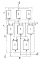
Zum sicheren Regenerieren und Synchronisieren eines digitalen Signales hoher Bitrate weist die erfindungsgemäße Schaltungsanordnung, wie in Figur 1 dargestellt, eine Reihenschaltung aus einer steuerbaren Verzögerungsleitung VZL und einer Entscheidungslogik EL auf. Die Entscheidungslogik EL ist über eine erste Steuerleitung UPO und eine zweite Steuerleitung DOWNO und die steuerbare Verzögerungsleitung VZL über Adressenleitungen S0, S1, S2, S3 an eine Verzögerungsregeleinheit VRE angeschlossen. Dabei enthält die Verzögerungsregeleinheit VRE einen voreinstellbaren Eingang PR, über den sie auf vorgebbare Zustände gesetzt werden kann.For safe regeneration and synchronization of a high bit rate digital signal, the circuit arrangement according to the invention, as shown in FIG. 1, has a series circuit comprising a controllable delay line VZL and a decision logic EL. The decision logic EL is connected to a delay control unit VRE via a first control line UPO and a second control line DOWNO and the controllable delay line VZL via address lines S0, S1, S2, S3. The delay control unit VRE contains a presettable input PR, via which it can be set to predefinable states.
Die Entscheidungslogik EL weist eine an eine Taktleitung TL angeschlossene Abtastschaltung AS und eine Auswerteeinheit AWE auf.The decision logic EL has a sampling circuit AS connected to a clock line TL and an evaluation unit AWE.
Über die Taktleitung TL wird die Abtastschaltung mit einem Systemtakt CK versorgt, dessen Frequenz der Bitrate des zu regenerierenden und synchronisierenden digitalen Signales entspricht.The sampling circuit is supplied with a system clock CK via the clock line TL, the frequency of which corresponds to the bit rate of the digital signal to be regenerated and synchronized.
Im vorliegenden Ausführungsbeispiel beträgt die Frequenz des Systemtaktes CK 139,264 MHz.In the present exemplary embodiment, the frequency of the system clock CK is 139.264 MHz.
Die Auswerteeinheit AWE besteht aus einer Dekodiereinheit DEC und einem Entscheider ENT die untereinander über fünf Zustandsleitungen U, D, O, F1, F2 verbunden sind. Weiterhin weist der Entscheider ENT der Auswerteeinheit AWE einen ersten Zustandsanzeigeausgang Z0 und einen zweiten Zustandsanzeigeausgang Z1 auf und ist über eine erste Leitung BU und eine zweite Leitung BD an die steuerbare Verzögerungsleitung VZL angeschlossen.The evaluation unit AWE consists of a decoding unit DEC and a decision maker ENT which are connected to one another via five status lines U, D, O, F1, F2. Furthermore, the decision maker ENT of the evaluation unit AWE has a first status display output Z0 and a second status display output Z1 and is connected to the controllable delay line VZL via a first line BU and a second line BD.
Ferner ist der Entscheider ENT über die erste UPO und die zweite Steuerleitung DOWNO an einen Eingang VE für die Vorwärtszählrichtung bzw. an einen Eingang RE für die Rückwärtszählrichtung eines Vorwärts-Rückwärts-Zählers VRZ der Verzögerungsregeleinheit VRE angeschlossen. Der Entscheider ENT und der Vorwärts-Rückwärts-Zähler VRZ werden dabei mit einem internen Takt TI versorgt, der aus dem Systemtakt CK abgeleitet wird.Furthermore, the decision maker ENT is via the first UPO and the second control line DOWNO to an input VE for the up-count direction or to an input RE for the down-count direction of an up-down counter VRZ the delay control unit VRE connected. The decision maker ENT and the up-down counter VRZ are supplied with an internal clock TI, which is derived from the system clock CK.
Hier ist die Frequenz des internen Taktes TI 1/8-mal so groß, wie die Frequenz des Systemtaktes CK.Here the frequency of the internal clock TI is 1/8 times as high as the frequency of the system clock CK.
Ausgänge A0, A1, A2, A3 des Vorwärts-Rückwärts-Zählers VRZ sind über die Adressenleitungen S0, S1, S2, S3 mit der steuerbaren Verzögerungsleitung VZL verbunden.Outputs A0, A1, A2, A3 of the up-down counter VRZ are connected to the controllable delay line VZL via the address lines S0, S1, S2, S3.
Die Abtastschaltung AS, wie in Figur 2 gezeigt, besteht aus einem dreistufigen Phasenschieber PS und einer aus fünf Zwischenspeicher FF1, FF2, FF3, FFM, FFB aufgebauten Abtast/Speichereinheit ASPE.The sampling circuit AS, as shown in FIG. 2, consists of a three-stage phase shifter PS and a sampling / storage unit ASPE constructed from five buffers FF1, FF2, FF3, FFM, FFB.
Dabei ist ein Ausgang P1 der ersten Stufe des Phasenschiebers PS mit einem Dateneingang D1 des ersten Zwischenspeichers FF1, ein Ausgang P2 der zweiten Stufe des Phasenschiebers PS mit einem Dateneingang D2 des zweiten Zwischenspeichers FF2 und parallel dazu mit einem Dateneingang DM des vierten Zwischenspeichers FFM verbunden. Ein Ausgang P3 der dritten Stufe des Phasenschiebers PS ist mit einem Dateneingang D3 des dritten Zwischenspeichers FF3 verbunden.An output P1 of the first stage of the phase shifter PS is connected to a data input D1 of the first buffer store FF1, an output P2 of the second stage of the phase shifter PS is connected to a data input D2 of the second buffer store FF2 and, in parallel, to a data input DM of the fourth buffer store FFM. An output P3 of the third stage of the phase shifter PS is connected to a data input D3 of the third buffer FF3.
Ein Datenausgang Q2 des zweiten Zwischenspeichers FF2, der gleichzeitig auch den Datenausgang der Entscheidungslogik EL bildet, ist an einen Dateneingang DB des fünften Zwischenspeichers FFB angeschlossen. Weiterhin ist ein Datenausgang Q1, Q2, Q3, QM, QB jedes Zwischenspeichers FF1, FF2, FF3, FFM, FFB mit der Dekodiereinheit DE der Auswerteeeinheit AWE verbunden (vgl. Figur 1). Jeder Zwischenspeicher FF1, FF2, FF3, FFM, FFB ist über einen Takteingang T1, T2, T3, TM, TB parallel an die Taktleitung TL angeschlossen, wobei der vierte Zwischenspeicher FFM einen invertierenden Takteingang TM aufweist. Die getakteten Zwischenspeicher werden durch sogenannte D-Flip-Flops realisiert.A data output Q2 of the second buffer FF2, which also forms the data output of the decision logic EL, is connected to a data input DB of the fifth buffer FFB. Furthermore, there is a data output Q1, Q2, Q3, QM, QB of each buffer FF1, FF2, FF3, FFM, FFB connected to the decoding unit DE of the evaluation unit AWE (see FIG. 1). Each buffer store FF1, FF2, FF3, FFM, FFB is connected in parallel to the clock line TL via a clock input T1, T2, T3, TM, TB, the fourth buffer store FFM having an inverting clock input TM. The clocked buffers are implemented by so-called D flip-flops.
In einer ersten Realisierung des Phasenschiebers PS, wie in Figur 2 gezeigt, werden drei Laufzeitglieder LZG1, LZG2, LZG3 verwendet, die von dem ankommenden digitalen Signal parallel durchlaufen werden. Die kleinste Phasendifferenz wird dabei durch die kleinste Laufzeitdifferenz zweier Laufzeitglieder bestimmt. Unabhängig von Laufzeittoleranzen muß somit immer die Phasenverschiebung φ1 durch das erste Laufzeitglied LZG1 kleiner als die Phasenverschiebung durch das zweite Laufzeitglied LZG2 und diese wieder kleiner als die Phasenverschiebung durch das dritte Laufzeitglied LZG3 sein. Die Laufzeitglieder können durch Leitungen einer gewissen Länge, durch ein Schieberegister oder aber durch einfache Logikgatter realisiert werden. In einer zweiten Realisierung des Phasenschiebers PS gemäß einer weiteren erfindungsgemäßen Ausgestaltung (nicht weiter gezeigt), sind zwei Laufzeitglieder LZG1, LZG2 in Reihe geschaltet. Ein vor dem ersten Laufzeitglied LZG1 angeordneter Abgriff bildet den Ausgang P1 der ersten Stufe, ein zwischen dem ersten LZG1 und dem zweiten Laufzeitglied LZG2 angeordneter Abgriff bildet den Ausgang P2 der zweiten Stufe und ein nach dem zweiten Laufzeitglied LZG2 angeordneter Abgriff bildet den Ausgang P3 der dritten Stufe des Phasenschiebers PS. Da das ankommende digitale Signal die drei Stufen seriell durchläuft, ist stets φ1 < φ2 < φ3 gegeben. Hier ist die kleinste Phasendifferenz Δφ = φ2 - φ1 oder φ3 - φ2 durch die minimal realisierbare Laufzeit der Laufzeitglieder LZG1, LZG2 bestimmt.In a first implementation of the phase shifter PS, as shown in FIG. 2, three delay elements LZG1, LZG2, LZG3 are used, which are passed through in parallel by the incoming digital signal. The smallest phase difference is determined by the smallest delay difference between two delay elements. Regardless of runtime tolerances, the phase shift φ1 by the first runtime element LZG1 must therefore always be smaller than the phase shift by the second runtime element LZG2 and this again smaller than the phase shift by the third runtime element LZG3. The delay elements can be implemented by lines of a certain length, by a shift register or by simple logic gates. In a second implementation of the phase shifter PS according to a further embodiment according to the invention (not shown further), two delay elements LZG1, LZG2 are connected in series. A tap arranged in front of the first runtime element LZG1 forms the output P1 of the first stage, a tap arranged between the first LZG1 and the second runtime element LZG2 forms the output P2 of the second stage, and a tap arranged after the second runtime element LZG2 forms the output P3 of the third Stage of the phase shifter PS. Since the incoming digital signal passes through the three stages in series, φ1 <φ2 <φ3 is always given. Here the smallest phase difference Δφ = φ2 - φ1 or φ3 - φ2 is determined by the minimum realizable runtime of the delay elements LZG1, LZG2.
Das ankommende digitale Signal wird über die steuerbare Verzögerungsleitung VZL zur Entscheidungslogik EL übertragen. Hier durchläuft es den dreistufigen Phasenschieber PS und wird durch den ersten, zweiten, dritten und vierten Zwischenspeicher FF1, FF2, FF3, FFM abgetastet und abgespeichert. Das Einlesen erfolgt mit der aktiven Flanke des Systemtaktes CK, wobei durch den invertierenden Takteingang TM des vierten Zwischenspeichers FFM, dieser eine halbe Systemtaktperiode T/2 früher und zwar mit der passiven Flanke den anliegenden Signalwert übernimmt.The incoming digital signal is transmitted to the decision logic EL via the controllable delay line VZL. Here it passes through the three-stage phase shifter PS and is scanned and stored by the first, second, third and fourth buffer stores FF1, FF2, FF3, FFM. The reading is carried out with the active edge of the system clock CK, whereby the inverting clock input TM of the fourth buffer FFM takes it over half a system clock period T / 2 earlier, with the passive edge taking over the signal value present.
Da der Dateneingang DB des fünften Zwischenspeichers FFB mit dem Datenausgang Q2 des zweiten Zwischenspeichers FF2 verbunden ist, übernimmt der fünfte Zwischenspeicher FFB mit jeder aktiven Systemtaktflanke den eine Systemtaktperiode T vorher abgetasteten Signalwert.Since the data input DB of the fifth buffer store FFB is connected to the data output Q2 of the second buffer store FF2, the fifth buffer store FFB takes over the signal value sampled one system clock cycle period T with each active system clock edge.
Die fünf Zwischenspeicher FF1, FF2, FF3, FFM, FFB liefern mit der aktiven Systemtaktflanke an ihren Datenausgängen Q1, Q2, Q3, QM, QB somit fünf Signale, die dem Datensignal zu den Zeiten t+Δt, t, t-Δt, t-T/2, t-T, entsprechen, wobei am Datenausgang Q2 des zweiten Zwischenspeichers FF2 das regenerierte Datensignal abgreifbar ist. Der Wert Δt ergibt sich entsprechend aus der Verzögerung der Laufzeitglieder LZG1, LZG2, LZG3 des Phasenschiebers PS und mit T ist die Systemtaktperiode angegeben.The five buffers FF1, FF2, FF3, FFM, FFB with the active system clock edge at their data outputs Q1, Q2, Q3, QM, QB thus provide five signals that correspond to the data signal at times t + Δt, t, t-Δt, tT / 2, tT, where the regenerated data signal can be tapped at the data output Q2 of the second buffer store FF2. The value .DELTA.t results accordingly from the delay of the delay elements LZG1, LZG2, LZG3 of the phase shifter PS and T is the system clock period.
Diese fünf Datensignale liegen nun an der Dekodiereinheit DEC der Auswerteeinheit AWE an und werden entsprechend der nachstehenden Wahrheitstabelle der Dekodiereinheit DEC - Tabelle 1 - dekodiert.

Für den Fall, daß die an den Datenausgängen Q1, Q2 und Q3 der ersten drei Zwischenspeicher FF1, FF2, FF3 anliegende Signale unterschiedliche Polaritäten aufweisen - siehe obere Tabellenhälfte - wird entweder die erste Zustandsleitung U oder die zweite Zustandsleitung D mit einem logischen "Eins"-Pegel beaufschlagt, wobei die logischen Zustände der anderen Zustandsleitungen ihren bisherigen Wert beibehalten. Dabei bedeutet eine Belegung der ersten Zustandsleitung U, daß das ankommende digitale Signal in Bezug zum Systemtakt CK eine Verzögerung und eine Belegung der zweiten Zustandsleitung D, daß das ankommende digitale Signal eine Beschleunigung erfahren muß, um jeweils synchron mit dem Systemtakt CK zu sein.In the event that the signals present at the data outputs Q1, Q2 and Q3 of the first three buffers FF1, FF2, FF3 have different polarities - see upper half of the table - either the first status line U or the second status line D is assigned a logical "one" -Level applied, whereby the logic states of the other state lines retain their previous value. An assignment of the first status line U means that the incoming digital signal is delayed in relation to the system clock CK, and an assignment of the second status line D means that the incoming digital signal must experience an acceleration in order to be synchronous with the system clock CK.
Falls nun zu den Zeiten ![]()
![]()
![]()
![]()
![]()
![]()
Erfindungsgemäß wird nun auch ein verzerrtes Signal mit unterschiedlichen (High-Low) Pulsbreiten richtig ausgewertet, wie aus der unteren Hälfte der Tabelle 1 ersichtlich, in dem zusätzlich zu den Zeiten t₁, t₂, t₃ noch eine halbe Systemtaktperiode T/2 früher - Zeipunkt tM - und eine ganze Systemtaktperiode T früher - Zeitpunkt tB - das digitale Signal abgetastet wird. Dabei entspricht das Signal am Ausgang QM des vierten Zwischenspeichers FFM dem Abtastwert zum Zeitpunkt tM und das Signal am Ausgang QB des fünften Zwischenspeicher FFB dem Abtastwert zum Zeitpunkt tB. Wird zum Zeitpunkt tB in Bezug zu den Zeitpunkten t₁, t₂, t₃ eine steigende Flanke detektiert, so wird die vierte Zustandsleitung F1 mit einem logischen "Eins"-Pegel beaufschlagt und entsprechend einer detektierten fallenden Flanke wird die fünfte Zustandsleitung F2 mit einem logischen "Eins"-Pegel belegt.According to the invention, a distorted signal with different (high-low) pulse widths is now correctly evaluated, as can be seen from the lower half of Table 1, in which, in addition to the
Sollte der Abtastwert zum Zeitpunkt tB mit den Abtast werten zu den Zeiten t₁, t₂, t₃ übereinstimmen und der Abtastwert zum Zeitpunkt tM eine andere Polarität aufweisen, so wird die dritte Zustandsleitung O mit einem logischen "Eins"-Pegel belegt. Somit wird, wie in Figur 5 Darstellung c) gezeigt, durch die zusätzlichen Signalzustände zu den Zeitpunkten tB und tM ein möglicher falscher Abtastzeitpunkt aufgrund unterschiedlicher Pulsbreiten des Signales erkannt.Should the sample at time t B match the samples at
Der in Tabelle 1 aufgezeigte Wert QR wird später noch erläutert.The QR value shown in Table 1 will be explained later.
Die durch die Dekodiereinheit DEC dekodierten Systemtakt-Daten-Phasenbeziehungen werden über die fünf Zustandsleitungen U, D, O, F1, F2 zum Entscheider ENT übertragen, der zusätzlich das Vorliegen einer Minimalverzögerung oder einer Maximalverzögerung der Verzögerungsleitung VZL auswertet, wozu er über die erste Leitung BU bzw. über die zweite Leitung BD mit der steuerbaren Verzögerungsleitung VZL verbunden ist.The system clock data phase relationships decoded by the decoding unit DEC are transmitted via the five status lines U, D, O, F1, F2 to the decision maker ENT, who additionally evaluates the presence of a minimum delay or a maximum delay of the delay line VZL, for which purpose it is transmitted via the first line BU or via the second line BD is connected to the controllable delay line VZL.
Gemäß dem in Figur 4 gezeigten Zustandsdiagramm des Entscheiders ENT sind vier Zustände zu unterscheiden, die der folgenden Tabelle zu entnehmen sind.

Die vier Zustände S, S2, S1, OS des Entscheiders ENT sind an dem ersten Zustandsanzeigeausgang Z0 und an den zweiten Zustandsanzeigeausgang Z1 jederzeit entnehmbar und können zur weiteren Überwachung, Testung oder Auswertung der erfindungsgemäßen Schaltungsanordnung auf eine entsprechende externe Einheit geleitet werden.The four states S, S2, S1, OS of the decision maker ENT can be removed at any time at the first status display output Z0 and at the second status display output Z1 and can be directed to a corresponding external unit for further monitoring, testing or evaluation of the circuit arrangement according to the invention.
Entsprechend der im folgenden gezeigten Tabelle 3 wird durch den Entscheider ENT in Abhängigkeit der anliegenden Eingangsvariablen, die über die fünf Zustandsleitungen U, D, O, F1, F2, sowie über die erste Leitung BU und die zweite Leitung BD anliegen, ein Steuersignal über die erste Steuerleitung UPO oder die zweite Steuerleitung DOWNO zur Verzögerungsregeleinheit VRE gesendet.

Aufgrund einer detektierten falschen Systemtakt-Daten-Phasenbeziehung, z.B. gemäß der laufenden Nummer 1 in der Tabelle 3, wird über die erste Steuerleitung UPO ein Zählimpuls auf den Eingang VE für die Vorwärtszählrichtung des Vorwärts-Rückwärts-Zählers VRZ gegeben. Nach Abgabe eines Zählimpulses über die erste Steuerleitung UPO werden durch den Entscheider ENT über eine auf die Dekodiereinheit DEC zurückgekoppelten Rücksetzleitung QR - vgl. Tabelle 1 linke Spalte - für die Dauer einer Taktperiode des internen Taktes TI die Dekodiereinheit DEC zurückgesetzt, um eine sichere Ausführung des Zählimpulses zu gewährleisten.Due to a detected incorrect system clock data phase relationship, e.g. According to the
Durch den Zählimpuls wird der Zählerstand des Vorwärts-Rückwärts- Zählers VRZ um Eins erhöht, wodurch sich eine Verzögerung der ankommenden digitalen Signale in Bezug auf den Systemtakt CK wie folgt ergibt.The counting pulse increases the count of the up-down counter VRZ by one, which results in a delay of the incoming digital signals with respect to the system clock CK as follows.
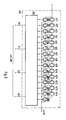
Dazu wird zunächst eine Realisierungsmöglichkeit der steuerbaren Verzögerungsleitung VZL gemäß Figur 3 beschrieben. Figur 3 zeigt eine aus vierzehn in Reihe geschalteten Verzögerungsgliedern VZ1, VZ2, ..., VZ14 aufgebaute Verzögerungsleitung VZL, wobei der O-te bis zu dem 14-ten Abgriff jeweils über einen ansteuerbaren Inverter IN0, IN1, ..., IN14 auf den Datenausgang der steuerbaren Verzögerungsleitung VZL geführt ist.For this purpose, a possible implementation of the controllable delay line VZL according to FIG. 3 is first described. FIG. 3 shows a delay line VZL constructed from fourteen delay elements VZ1, VZ2,..., VZ14 connected in series, the 0th to the 14th tap each having a controllable inverter IN0, IN1,..., IN14 the data output of the controllable delay line VZL is guided.
Zum Steuern der Verzögerungsleitung VZL ist eine Ansteuereinheit AST einerseits an die steuerbaren Inverter IN0, IN1, ..., IN14 und andererseits über die Adressenleitungen S0, S1, S2, S3 an die Ausgänge A0, A1, A2, A3 des Vorwärts-Rückwärts-Zählers VRZ angeschlossen.To control the delay line VZL, a control unit AST is connected on the one hand to the controllable inverters IN0, IN1, ..., IN14 and on the other hand via the address lines S0, S1, S2, S3 to the outputs A0, A1, A2, A3 of the forward-reverse VRZ meter connected.
Ist nun z.B. der Vorwärts-Rückwärts-Zähler VRZ über den voreinstellbaren Eingang PR auf den Zählerstand 7 eingestellt, so wird dieser Wert über die Adressenleitungen S0, S1, S2, S3 zur Ansteuereinheit AST übertragen, die genau den siebten Inverter IN7 durchsteuert, wobei gleichzeitig alle anderen Inverter für die Datenübertragung gesperrt sind. Das digitale Signal durchläuft also zunächst die ersten sieben Verzögerungsglieder VZ1, ..., VZ7, den siebten Inverter IN7 und gelangt über den Datenausgang der steuerbaren Verzögerungsleitung VZL zur Entscheidungslogik EL.Is now e.g. the up-down counter VRZ is set to the counter reading 7 via the presettable input PR, this value is transmitted via the address lines S0, S1, S2, S3 to the control unit AST, which controls exactly the seventh inverter IN7, at the same time all the other inverters are blocked for data transmission. The digital signal therefore first passes through the first seven delay elements VZ1,..., VZ7, the seventh inverter IN7 and reaches the decision logic EL via the data output of the controllable delay line VZL.
Wird nun, wie zuvor beschrieben, durch einen Zählimpuls über die erste Steuerleitung UPO der Zählerstand um Eins auf den Wert acht erhöht, so wird dies über die Adressenleitungen S0, S1, S2, S3 an die Ansteuereinheit AST weitergeleitet. Dadurch wird jetzt der achte Inverter IN8 durchgeschaltet, d.h alle anderen Inverter inklusive dem siebten Inverter IN7 sind gesperrt. Das digitale Signal wird nun um die Zeit eines weiteren Verzögerungsgliedes verzögert.If, as described above, the counter reading is increased by one to the value eight by a counting pulse via the first control line UPO, this is forwarded to the control unit AST via the address lines S0, S1, S2, S3. As a result, the eighth inverter IN8 is now switched through, i.e. all other inverters including the seventh inverter IN7 are blocked. The digital signal is now delayed by the time of another delay element.
Entsprechend wird ein Zählimpuls über die zweite Steuerleitung DOWNO durch den Entscheider ENT auf den Eingang RE des Vorwärts-Rückwärts-Zählers VRZ gegeben, wenn, wie z.B. gemäß der laufenden Nummer 14 in Tabelle 3,eine Beschleunigung des digitalen Signales erfolgen muß.Correspondingly, a counting pulse is given via the second control line DOWNO by the decision maker ENT to the input RE of the up-down counter VRZ if, e.g. According to serial number 14 in Table 3, the digital signal must be accelerated.
Aufgrund eines gesendeten logischen "0"-Zustandes, über die erste UPO und die zweite Steuerleitung DOWNO, wie z.B. gemäß der laufenden Nummer 2 in Tabelle 3, wird keine Verzögerungszeitänderung der steuerbaren Verzögerungsleitung VZL hervorgerufen.Due to a sent logic "0" state, via the first UPO and the second control line DOWNO, as for example in accordance with the
Außerdem ist ein gleichzeitiges Anlegen eines eine Verzögetung und eine Beschleunigung bewirkenden Zählimpulses über die Steuerleitungen UPO, DOWNO - wie Tabelle 3 zu entnehmen ist - nicht möglich.In addition, it is not possible to simultaneously apply a counting pulse causing deceleration and acceleration via the control lines UPO, DOWNO - as can be seen in Table 3.
Das Auswerten einer Minimal- oder einer Maximalverzögerung der Verzögerungsleitung durch den Entscheider ENT verhindert ein mögliches Schwingen der Verzögerungsleitung VZL zwischen einer maximalen Verzögerung (vierzehnter Inverter IN14 durchgeschaltet) und einer minimalen Verzögerung (nullter Inverter INO durchgeschaltet, d.h. kein Verzögerungsglied aktiviert).The evaluation of a minimum or a maximum delay of the delay line by the decision maker ENT prevents a possible oscillation of the delay line VZL between a maximum delay (fourteenth inverter IN14 switched through) and a minimum delay (zero inverter INO switched through, i.e. no delay element activated).
Die erfindungsgemäße Schaltungsanordnung arbeitet bei beliebigen Bitraten (typisch: 140 MBit/s) bis zu einer maximalen Bitrate mit einer minimalen Bitlänge von Tmin, die durch die zeitliche Auflösung der Abtastschaltung AS (Laufzeit bzw. Laufzeitdifferenz Δt der Laufzeitglieder LZG1, LZG2, LZG3), durch die zeitliche Auflösung der Verzögerungsleitung tVZL , durch die Abweichung ΔPw der Pulsbreite von der Bitlänge Tmin und durch die Flankensteilheit tRF gemäß der Beziehung
![]()
bestimmt wird.The circuit arrangement according to the invention operates at any bit rates (typically: 140 Mbit / s) up to a maximum bit rate with a minimum bit length of T min , which is determined by the temporal resolution of the sampling circuit AS (transit time or transit time difference Δt of the transit time elements LZG1, LZG2, LZG3) , by the temporal resolution of the delay line t VZL , by the deviation ΔPw of the pulse width from the bit length T min and by the edge steepness t RF according to the relationship
![]()
is determined.
Claims (7)
- A circuit arrangement for regenerating and synchronizing a digital signal of high bit rate comprising a series combination of a variable delay line (VZL) and a decision logic (EL) through which the digital signal passes, with the decision logic (EL) connected to a delay control unit (VRE) by a first control line (UPO) and a second control line (DOWNO), and the variable delay line (VZL) connected to the delay control unit (VRE) by address lines (S0, S1, S2, S3), the decision logic (EL) being supplied via a clock line (TL) with a system clock (CK) having a frequency equal to the bit rate of the digital signal to be regenerated, and the delay control unit (VRE) having a preset input (TR) for establishing a presettable condition,
characterized in that the decision logic (EL) contains a sampling circuit (AS), which is connected to the clock line (TL), and an evaluating facility (AWE) by which the digital signal is sampled at at least three successive sampling instants t - Δt, t, t + Δt, where Δt = sampling interval, and additionally at the instants t - T/2 and t - T, where T = system clock period, and subsequently determines on the basis of the at least three successive sampling instants whether a correct system-clock/data phase relationship exists, and on the basis of the additional instants whether there is any false sampling instant due to differing pulse widths of the signal, that the evaluating facility (AWE) has a first state-indicating output (Z0) and a second state-indicating output (Z1), and that the variable delay line (VZL) is connected to the evaluating facility (AWE) by a first line (BU) and a second line (BD) over which the presence of, respectively, a minimum delay and a maximum delay of the delay line (VZL) is communicated to the evaluating facility (AWE). - A circuit arrangement as claimed in claim 1, characterized in that the sampling circuit (AS) contains a three-stage phase shifter (PS) and a sample/hold unit (ASPE) consisting of five latches (FF1, FF2, FF3, FFM, FFB), that an output (P1) of the first stage of the phase shifter (PS) is connected to a data input (D1) of the first latch (FF1), that an output (P2) of the second stage of the phase shifter (PS) is connected to a data input (D2) of the second latch (FF2) and to a data input (DM) of the fourth latch (FFM), that an output (P3) of the third stage of the phase shifter (PS) is connected to a data input (D3) of the third latch (FF3), that a data output (Q2) of the second latch (FF2), which forms the data output of the decision logic (EL), is connected to a data input (DB) of the fifth latch (FFB), that a data output (Q1, Q2, Q3, QM, QB) of each of the latches (FF1, FF2, FF3, FFM, FFB) is connected to the evaluating facility (AWE), and that each of the latches (FF1, FF2, FF3, FFM, FFB) has a clock input (T1, T2, T3, TM, TB) connected to the clock line (TL) in parallel, with the clock input (TM) of the fourth latch (FFM) being an inverting input.
- A circuit arrangement as claimed in claim 2, characterized in that the evaluating facility (AWE) contains a decoder unit (DEC) and a decision unit (ENT), that the decoder unit (DEC) has one end connected to the data outputs (Q1, Q2, Q3, QM, QB) of the latches (FF1, FF2, FF3, FFM, FFB) of the sample/hold unit (ASPE), that the other end of the decoder unit (DEC) is connected to the decision unit (ENT) by five state lines (U, D, O, F1, F2) for transferring the decoded signal states, and that the decision unit (ENT) is connected to the delay control unit (VRE) by the first control line (UPO) and the second control line (DOWNO), and to the variable delay line (VZL) by the first line (BU) and the second line (BD), so that the respective phase relationship between the signal and the system clock can be obtained from the first state-indicating output (Z0) and the second state-indicating output (Z1) of the decision unit (ENT).
- A circuit arrangement as claimed in claim 3, characterized in that the decision unit (ENT) and the delay control unit (VRE) are supplied with an internal clock (TI) derived from the system clock (TK), and that the decision unit (ENT) is coupled to the decoder unit (DEC) via a preset line (QR), so that, when a control signal is sent out over the first (UPO) or second control line (DOWNO), the decoder unit (DEC) is reset for one period of the internal clock (TI).
- A circuit arrangement as claimed in claim 2, characterized in that the three stages of the phase shifter (PS) are implemented with delay elements (LZG1, LZG2, LZG3) through which the incoming digital signal passes in parallel, with the phase shift produced by the first delay element (LZG1) being smaller than the phase shift produced by the second delay element (LZG2), and with the phase shift produced by the second delay element (LZG2) being smaller than the phase shift produced by the third delay element (LZG3).
- A circuit arrangement as claimed in claim 2, characterized in that the phase shifter (PS) comprises two delay elements (LZG1, LZG2) in series, with a tap ahead of the first delay element (LZG1) forming the output (P1) of the first stage of the phase shifter (PS), a tap between the first delay element (LZG1) and the second delay element (LZG2) forming the output (P2) of the second stage, and a tap behind the second delay element (LZG2) forming the output (P3) of the third stage, so that the incoming digital signal passes through the three stages in succession.
- A circuit arrangement as claimed in claim 3, characterized in that the delay control unit (VRE) comprises a synchronous up/down counter (VRZ) connected to the internal clock (TI) and having the preset input (PR), that the first control line (UPO) and the second control line (DOWNO) are connected,respectively, to an up input (VE) and a down input (RE) of the up/down counter (VRZ), and that the variable delay line (VZL) is connected to the outputs (A0, A1, A2, A3) of the up/down counter (VRZ) via the address lines (S0, S1, S2, S3).
Applications Claiming Priority (2)
| Application Number | Priority Date | Filing Date | Title |
|---|---|---|---|
| DE19853543392 DE3543392A1 (en) | 1985-12-07 | 1985-12-07 | CIRCUIT ARRANGEMENT FOR REGENERATING AND SYNCHRONIZING A DIGITAL SIGNAL |
| DE3543392 | 1985-12-07 |
Publications (3)
| Publication Number | Publication Date |
|---|---|
| EP0225587A2 EP0225587A2 (en) | 1987-06-16 |
| EP0225587A3 EP0225587A3 (en) | 1991-04-10 |
| EP0225587B1 true EP0225587B1 (en) | 1993-02-24 |
Family
ID=6287968
Family Applications (1)
| Application Number | Title | Priority Date | Filing Date |
|---|---|---|---|
| EP19860116757 Expired - Lifetime EP0225587B1 (en) | 1985-12-07 | 1986-12-02 | Circuit arrangement for regenerating and synchronising a digital signal |
Country Status (3)
| Country | Link |
|---|---|
| EP (1) | EP0225587B1 (en) |
| DE (2) | DE3543392A1 (en) |
| ES (1) | ES2003961A6 (en) |
Families Citing this family (9)
| Publication number | Priority date | Publication date | Assignee | Title |
|---|---|---|---|---|
| DE3702614A1 (en) * | 1987-01-29 | 1988-08-11 | Standard Elektrik Lorenz Ag | DIGITAL COUPLING NETWORK FOR LINE AND PACKAGE SWITCHING AND COUPLING DEVICE TO THIS |
| BE1000512A7 (en) * | 1987-05-07 | 1989-01-10 | Bell Telephone Mfg | Switching network. |
| EP0364451A1 (en) * | 1988-03-26 | 1990-04-25 | BELL TELEPHONE MANUFACTURING COMPANY Naamloze Vennootschap | Synchronizing circuit |
| DE3931259A1 (en) * | 1989-09-19 | 1991-03-28 | Siemens Ag | Continual matching of digital signal to clock - using output of second tapped delay line to control selection of tap on first line |
| DE59008700D1 (en) * | 1989-09-19 | 1995-04-20 | Siemens Ag | Synchronizer for a digital signal. |
| DE4025004A1 (en) * | 1990-08-07 | 1992-02-13 | Standard Elektrik Lorenz Ag | CIRCUIT ARRANGEMENT FOR REGENERATING AND SYNCHRONIZING A DIGITAL SIGNAL |
| EP0562183A1 (en) * | 1992-03-27 | 1993-09-29 | ALCATEL BELL Naamloze Vennootschap | Synchronization method and device realizing said method |
| DE4434803C1 (en) * | 1994-09-29 | 1996-03-07 | Ant Nachrichtentech | Serial bit stream sampling method for high speed data transmission equipment |
| US6130566A (en) * | 1996-10-30 | 2000-10-10 | Yokomizo; Akira | Digital wave shaping circuit, frequency multiplying circuit, and external synchronizing method, and external synchronizing circuit |
Family Cites Families (1)
| Publication number | Priority date | Publication date | Assignee | Title |
|---|---|---|---|---|
| DE3441501A1 (en) * | 1984-11-14 | 1986-05-15 | Standard Elektrik Lorenz Ag, 7000 Stuttgart | Circuit arrangement for regenerating and synchronising a digital signal |
-
1985
- 1985-12-07 DE DE19853543392 patent/DE3543392A1/en not_active Withdrawn
-
1986
- 1986-12-02 DE DE8686116757T patent/DE3687825D1/en not_active Expired - Fee Related
- 1986-12-02 EP EP19860116757 patent/EP0225587B1/en not_active Expired - Lifetime
- 1986-12-05 ES ES8603299A patent/ES2003961A6/en not_active Expired
Also Published As
| Publication number | Publication date |
|---|---|
| ES2003961A6 (en) | 1988-12-01 |
| DE3687825D1 (en) | 1993-04-01 |
| EP0225587A3 (en) | 1991-04-10 |
| DE3543392A1 (en) | 1987-06-25 |
| EP0225587A2 (en) | 1987-06-16 |
Similar Documents
| Publication | Publication Date | Title |
|---|---|---|
| DE69106012T2 (en) | Frame synchronization arrangement. | |
| DE68923207T2 (en) | Circuit for preventing a metastable state. | |
| DE69016169T2 (en) | Line interface for a communications network. | |
| DE3246432C2 (en) | ||
| EP0225587B1 (en) | Circuit arrangement for regenerating and synchronising a digital signal | |
| EP0345564B1 (en) | Method and device for the recuperation of a bit clock from a digital telecommunication signal | |
| DE3442613C2 (en) | ||
| DE60213443T2 (en) | MEMORY SWITCHING AND CIRCUIT FOR DETECTING A VALID TRANSITION | |
| DE3686902T2 (en) | SELF-TESTING TWO-CHANNEL RISING FLANGE SYNCHRONIZER. | |
| CH651709A5 (en) | METHOD AND DEVICE FOR EQUALIZING BINARY RECEPTION SIGNALS. | |
| DE2055356B2 (en) | GRID SYNCHRONIZATION CIRCUIT FOR DIGITAL COMMUNICATION SYSTEMS | |
| DE69120244T2 (en) | Synchronization circuit | |
| EP0363513A1 (en) | Method and apparatus for receiving a binary digital signal | |
| DE3441501A1 (en) | Circuit arrangement for regenerating and synchronising a digital signal | |
| DE1252727B (en) | Procedure for the interference-free reception of transmitted data | |
| DE2714219C2 (en) | ||
| DE102004044815A1 (en) | Data processing device with clock recovery from different sources | |
| EP0545493A2 (en) | Scanning circuit | |
| EP0317829B1 (en) | Method and apparatus for the generation of a correcting signal for a digital clock recovery device | |
| DE2242639B2 (en) | TIME MULTIPLEX TELEGRAPHY SYSTEM FOR NESTING BY CHARACTER | |
| DE3246211A1 (en) | Circuit arrangement for detecting sequences of identical binary values | |
| DE3924907A1 (en) | REDUNDANT CLOCK ARRANGEMENT | |
| DE69412332T2 (en) | Method for accelerating the synchronization of a phase locked loop and corresponding phase locked loop | |
| DE19535007A1 (en) | Counter circuit with charging function | |
| DE2030763A1 (en) | Digital code converter for ternary codes |
Legal Events
| Date | Code | Title | Description |
|---|---|---|---|
| PUAI | Public reference made under article 153(3) epc to a published international application that has entered the european phase |
Free format text: ORIGINAL CODE: 0009012 |
|
| AK | Designated contracting states |
Kind code of ref document: A2 Designated state(s): BE DE FR IT NL |
|
| RAP1 | Party data changed (applicant data changed or rights of an application transferred) |
Owner name: ALCATEL N.V. Owner name: STANDARD ELEKTRIK LORENZ AKTIENGESELLSCHAFT |
|
| RAP3 | Party data changed (applicant data changed or rights of an application transferred) |
Owner name: ALCATEL N.V. Owner name: STANDARD ELEKTRIK LORENZ AKTIENGESELLSCHAFT |
|
| PUAL | Search report despatched |
Free format text: ORIGINAL CODE: 0009013 |
|
| AK | Designated contracting states |
Kind code of ref document: A3 Designated state(s): BE DE FR IT NL |
|
| 17P | Request for examination filed |
Effective date: 19910719 |
|
| 17Q | First examination report despatched |
Effective date: 19911119 |
|
| RAP3 | Party data changed (applicant data changed or rights of an application transferred) |
Owner name: ALCATEL N.V. Owner name: ALCATEL SEL AKTIENGESELLSCHAFT |
|
| GRAA | (expected) grant |
Free format text: ORIGINAL CODE: 0009210 |
|
| AK | Designated contracting states |
Kind code of ref document: B1 Designated state(s): BE DE FR IT NL |
|
| ITF | It: translation for a ep patent filed | ||
| REF | Corresponds to: |
Ref document number: 3687825 Country of ref document: DE Date of ref document: 19930401 |
|
| ET | Fr: translation filed | ||
| PGFP | Annual fee paid to national office [announced via postgrant information from national office to epo] |
Ref country code: BE Payment date: 19931223 Year of fee payment: 8 |
|
| PLBE | No opposition filed within time limit |
Free format text: ORIGINAL CODE: 0009261 |
|
| STAA | Information on the status of an ep patent application or granted ep patent |
Free format text: STATUS: NO OPPOSITION FILED WITHIN TIME LIMIT |
|
| 26N | No opposition filed | ||
| PG25 | Lapsed in a contracting state [announced via postgrant information from national office to epo] |
Ref country code: BE Effective date: 19941231 |
|
| BERE | Be: lapsed |
Owner name: ALCATEL N.V. Effective date: 19941231 |
|
| PGFP | Annual fee paid to national office [announced via postgrant information from national office to epo] |
Ref country code: NL Payment date: 20011120 Year of fee payment: 16 |
|
| PGFP | Annual fee paid to national office [announced via postgrant information from national office to epo] |
Ref country code: DE Payment date: 20011208 Year of fee payment: 16 |
|
| PGFP | Annual fee paid to national office [announced via postgrant information from national office to epo] |
Ref country code: FR Payment date: 20011211 Year of fee payment: 16 |
|
| PG25 | Lapsed in a contracting state [announced via postgrant information from national office to epo] |
Ref country code: NL Free format text: LAPSE BECAUSE OF NON-PAYMENT OF DUE FEES Effective date: 20030701 Ref country code: DE Free format text: LAPSE BECAUSE OF NON-PAYMENT OF DUE FEES Effective date: 20030701 |
|
| NLV4 | Nl: lapsed or anulled due to non-payment of the annual fee |
Effective date: 20030701 |
|
| PG25 | Lapsed in a contracting state [announced via postgrant information from national office to epo] |
Ref country code: FR Free format text: LAPSE BECAUSE OF NON-PAYMENT OF DUE FEES Effective date: 20030901 |
|
| REG | Reference to a national code |
Ref country code: FR Ref legal event code: ST |
|
| PG25 | Lapsed in a contracting state [announced via postgrant information from national office to epo] |
Ref country code: IT Free format text: LAPSE BECAUSE OF NON-PAYMENT OF DUE FEES;WARNING: LAPSES OF ITALIAN PATENTS WITH EFFECTIVE DATE BEFORE 2007 MAY HAVE OCCURRED AT ANY TIME BEFORE 2007. THE CORRECT EFFECTIVE DATE MAY BE DIFFERENT FROM THE ONE RECORDED. Effective date: 20051202 |