EP0224901A2 - High resolution optical fiber array and article position determining system - Google Patents
High resolution optical fiber array and article position determining system Download PDFInfo
- Publication number
- EP0224901A2 EP0224901A2 EP86116651A EP86116651A EP0224901A2 EP 0224901 A2 EP0224901 A2 EP 0224901A2 EP 86116651 A EP86116651 A EP 86116651A EP 86116651 A EP86116651 A EP 86116651A EP 0224901 A2 EP0224901 A2 EP 0224901A2
- Authority
- EP
- European Patent Office
- Prior art keywords
- light
- array
- fibers
- fiber
- optical
- Prior art date
- Legal status (The legal status is an assumption and is not a legal conclusion. Google has not performed a legal analysis and makes no representation as to the accuracy of the status listed.)
- Granted
Links
- 239000013307 optical fiber Substances 0.000 title abstract description 50
- 239000000835 fiber Substances 0.000 claims abstract description 54
- 238000003491 array Methods 0.000 claims abstract description 31
- 239000011159 matrix material Substances 0.000 claims abstract description 14
- 230000003287 optical effect Effects 0.000 claims description 44
- 238000005286 illumination Methods 0.000 claims description 11
- 238000004891 communication Methods 0.000 claims description 9
- 238000012546 transfer Methods 0.000 claims description 5
- 230000008878 coupling Effects 0.000 claims description 2
- 238000010168 coupling process Methods 0.000 claims description 2
- 238000005859 coupling reaction Methods 0.000 claims description 2
- 230000005540 biological transmission Effects 0.000 claims 2
- 238000012935 Averaging Methods 0.000 claims 1
- 238000004519 manufacturing process Methods 0.000 description 11
- 238000000034 method Methods 0.000 description 5
- 230000007704 transition Effects 0.000 description 5
- 238000004458 analytical method Methods 0.000 description 4
- 230000006870 function Effects 0.000 description 4
- 238000005516 engineering process Methods 0.000 description 3
- 239000007787 solid Substances 0.000 description 3
- 239000004593 Epoxy Substances 0.000 description 2
- 238000006243 chemical reaction Methods 0.000 description 2
- 239000004744 fabric Substances 0.000 description 2
- 238000012986 modification Methods 0.000 description 2
- 230000004048 modification Effects 0.000 description 2
- 238000012545 processing Methods 0.000 description 2
- 238000012360 testing method Methods 0.000 description 2
- 230000009471 action Effects 0.000 description 1
- 230000000903 blocking effect Effects 0.000 description 1
- 239000003990 capacitor Substances 0.000 description 1
- 230000003247 decreasing effect Effects 0.000 description 1
- 238000007429 general method Methods 0.000 description 1
- 238000007689 inspection Methods 0.000 description 1
- 230000001678 irradiating effect Effects 0.000 description 1
- 239000000463 material Substances 0.000 description 1
- 230000007246 mechanism Effects 0.000 description 1
- 230000008569 process Effects 0.000 description 1
- 238000011160 research Methods 0.000 description 1
- 238000005070 sampling Methods 0.000 description 1
Images


Classifications
-
- G—PHYSICS
- G01—MEASURING; TESTING
- G01B—MEASURING LENGTH, THICKNESS OR SIMILAR LINEAR DIMENSIONS; MEASURING ANGLES; MEASURING AREAS; MEASURING IRREGULARITIES OF SURFACES OR CONTOURS
- G01B11/00—Measuring arrangements characterised by the use of optical techniques
- G01B11/02—Measuring arrangements characterised by the use of optical techniques for measuring length, width or thickness
- G01B11/028—Measuring arrangements characterised by the use of optical techniques for measuring length, width or thickness by measuring lateral position of a boundary of the object
-
- G—PHYSICS
- G01—MEASURING; TESTING
- G01V—GEOPHYSICS; GRAVITATIONAL MEASUREMENTS; DETECTING MASSES OR OBJECTS; TAGS
- G01V8/00—Prospecting or detecting by optical means
- G01V8/10—Detecting, e.g. by using light barriers
- G01V8/20—Detecting, e.g. by using light barriers using multiple transmitters or receivers
- G01V8/24—Detecting, e.g. by using light barriers using multiple transmitters or receivers using optical fibres
Definitions
- a common technique used by these prior art vision systems is to take an N by M array representing the pixel elements of a view of the object and produce data representing this N by M array for analysis by a computer.
- an analysis usually requires extensive computer resources and time to complete the analysis. Therefore, the use of vision systems in real time computer operations for support of manufacturing processing has,been limited.
- U.S. Patent No. 4,105,925 entitled “Optical Object Locator” which discloses a device for determining the position and orientation of an object on a conveyor by the use of two planes of light that intersect in a single transverse line on a conveyor surface.
- a linear diode array that is aligned along the single line of light on the conveyor detects light from that line by electronic sampling of the lumination of this linear array.
- Object boundaries are determined and object shape and orientation may thus be determined.
- Another patent entitled “Light Collection Apparatus” disclosed in U.S. Patent No. 3,987,301 discloses an apparatus for detecting the presence of extraneous matter and/or _ cracks in translucent containers.
- the light collection apparatus incorporates an array of fiber optics elements arranged to perform an accurate and controllable method of light collection.
- This invention relates to automated vision systems for manufacturing and more particularly to a vision system for determining article positions during a manufacturing process.
- the first step in vision analysis by a machine vision device is the conversion of analog pixel (picture element) data into digital data for processing by a computer.
- analog pixel picture element
- the present invention has been embodied in an apparatus to provide vision information for a manufacturing environment.
- An object of the present invention is to provide a non-complex vision system that indicates the location and positioning of an article used in manufacture.
- a further object of the present invention is to provide a vision apparatus that provides a digital output without having to perform analog to digital data conversions.
- a further object of the present invention is to provide a vision apparatus that allows variations in optical resolution.
- a vision apparatus for detecting the presence of an object as the object passes across a lighted surface.
- At least one light receiving array is located on the surface of a path traveled by an object.
- This light receiving array includes a light transfer device for conducting light radiated upon the light receiving array to an optical sensor.
- the optical sensor produces an electrical signal indicating what portion of the light receiving array is receiving light.
- the apparatus includes several linear arrays located upon the surface of a work station. Articles of manufacture pass across this surface and over these arrays.
- the apparatus includes several linear arrays of optical fibers positioned such that one end of each of the optical fibers receives light along the surface of this work station area. The other ends of the optical fiber arrays are connected to a fixed matrix plate which is positioned in a camera enclosure to emit light through a lens system onto an optical sensor.
- the optical sensor is a random access memory which is continually read by a computational device to determine what portions of the random access memory device have been exposed to light.
- the individual optical fibers are collimated to emit light upon specific elements of the optical random access memory. Therefore, the illumination of a specific element of the random access memory directly correlates to the illumination of the location of that fiber element end upon the work station surface.
- the output from the memory is digital data indicating the edge locations of the articles upon the work station surface.
- the spacing between the fibers ends at the work station is different than the fiber end spacing at the camera enclosure end of the fiber optical fiber bundle.
- this invention is applied to a work place for manufacturing articles of clothing.
- the articles of manufacture are cloth material which are essentially two dimensional in nature.
- this invention is also capable of detecting the positional orientation of an article having three dimensions.
- the purpose of this invention is to provide digital data indicating the edge locations of these articles.
- an attached computer can determine the center of the article and-further can direct a robotic arm to the article to pickup the article wherein the article will be grasped in a known orientation.
- FIGURE 1 illustrates a work place 10 containing two articles of manufacture 12 and 14.
- these articles of manufacture 12 and 14 represent pockets for denim blue jeans:
- the object of the invention is to provide data representing the positional orientation of these pockets 12 and 14.
- the work station 10 includes several linear arrays 16, 18, 20, 22, 24, and 26.
- Each linear array includes an optical fiber ribbon 28 having a linear arrangement of optical fiber ends, as shown in FIGURE 2. -When the pockets 12 and 14 are positioned over these linear arrays, light is blocked from illuminating the optical fibers underneath the pockets.
- FIGURE 2 illustrates a symbolic view of the linear array 16 including the linear ribbon 28 of optical fiber ends.
- the optical fibers of linear array 16 are contained within an optical fiber bundle 30 which terminates in a second linear array 34 exposing the opposite ends of the optical fibers to provide an optical fiber ribbon 32.
- the ribbon 32 is optically coupled as illustrated by field of view 36 through a lens 40 to an optical RAM 42 that is contained within a camera enclosure 38.
- the linear array 34 is positioned on one end of the camera enclosure 38.
- the purpose of the camera enclosure 38 is to minimize the amount of extaneous light to the optical RAM 42.
- the optical RAM 42 provides binary data on lines 44 to indicate which of the fibers are receiving light.
- the length of ribbon 28 appears to be similar to the length of ribbon 32.
- bundle 30 consists of 256 optical fibers that terminate in a optical fiber ribbon 32 that is 2.56 inches in width.
- Ribbon 28, which is the work station end of bundle 30, is also 2.56 inches wide (i.e., 100 fibers per inch).
- the apparent resolution of the optical fiber system can be changed, even though the appearance of the fiber ribbons at the camera enclosure always remain the same.
- FIGURE 3 schematically illustrates the illumination of a portion of an optical fiber ribbon 28.
- the optical fiber ribbon 28 includes a length 45 of which only portion 46 receives light. Since the optical ribbon 28 is located in the surface of work place 10, light above the work place surface irradiating down upon the work space surface is blocked by work piece 12 from all but portion 46 of the optical fiber ribbon 28. As a result, only a portion 48 of the optical RAM 42 is illuminated through the lensing system 40. This action indicates one edge of the work piece 12. In a similar manner the other edges of the work piece are located. Thus, by using the three optical fiber ribbons of the arrays 16, 18 and 20, the position of work piece 12 upon work space 10 is determined.
- FIGURE 4 illustrates the coupling of the optical system of a preferred embodiment of the present invention.
- a work space 100 includes 6 linear arrays 106, 108, 110, 112, 114, and 116 each positioned on the work space surface.
- Work pieces 102 and 104 are illustrated at a position above the linear arrays as the work pieces travel across work space 100.
- Each of the linear arrays 106-116 are coupled to an optical fiber bundle 118 that terminates in an array matrix 120.
- the matrix 120 includes several linear optical fiber ribbons- 121-126, shown in Figure 5, corresponding to each of the linear arrays 106-116 of work place 100.
- a lens 132 provides a field of view 128 to transfer light from the array matrix 120 to an optical random access memory 134.
- FIGURE 5 more clearly illustrates the linear ribbons 121-126 within the array matrix 120 which is, in FIGURE 5, exploded from the left most end of the camera enclosure 130.
- the camera enclosure 130 is a light sealed structure that enables only the light from the linear ribbons 121-126 to enter the interior portion of the light enclosure 130 and illuminate the surface of the optical RAM 134.
- FIGURE 6 illustrates a cylinder 140 used to assemble the linear optical fiber ribbons 121-126.
- Cylinder 140 includes two relatively large circumferential grooves 142 and 143 and several relatively small circumferential grooves 144.
- the larger grooves 142 and 143 receive relatively large fibers (not shown) that serve as locational reference fibers.
- Smaller fibers (not shown) are positioned in grooves 144 as light transmitting fibers.
- a longitudinal channel 145 is provided along a portion of the perphery of cylinder 140 to receive a mold (not shown). When the fibers are in place in grooves 142, 143 and 144, the mold is assembled by way of channel 145 underneath and above the fibers in grooves 142, 143, and 144.
- Epoxy is injected under pressure into this mold to seal the relative positions of the fibers in grooves 142, 143, and 144 relative to one another.
- the mold and fiber bundle are removed removed from cylinder 140.
- the mold is then removed from the optical fiber ribbon assembly and the ends of this ribbon assembly are appropriately machined and surfaced by conventional means to permit reception or emission of light.
- the epoxied fiber bundle is then assembled in a linear array structure at the work place or at the matrix plate, the reference fibers which were in grooves 142 and 143 serving as the means to locate the optical fibers which were in grooves 144.
- the matrix plate 120 of FIGURE 5 is replaced by a solid plate that includes selectively drilled holes to receive individual optical fibers. Once these fibers have been assembled in their respective holes, the optical fiber bundle is sealed and fixed to the matrix plate 120 in a conventional manner that will not interfere with the light transmissivity property of the individual fibers.
- FIGURE 7 illustrates a longitudinal cross-sectional view of cylinder 140 of FIGURE 6 showing the optical fiber arrangement.
- Reference fibers 151 and 152 are provided in their respective grooves 143 and 142.
- Intermediate optical fibers 153 and 154 are provided in two separate layers. As shown, eight fibers 153 lie in spaced apart grooves 144. Eight fibers 154 are each positioned between two of fibers 153 on ridges 156. The purpose for this configuration of optical fibers is explained by reference to FIGURE 8.
- FIGURE 8 illustrates one aspect of a preferred embodiment of the optical random acess memory 134.
- Optical memory elements 160 are positioned in two rows upon the surface of the optical random access memory 134.
- the specific topology of optical random access memory 134 requires that a linear optical fiber array such as that of FIGURE 7 illuminate circular portions 162 and 164 of memory elements 160. This illumination occurs by focusing individual light elements onto portions 162 and 164 of the array, as illustrated at FIGURE 8.
- Light striking a particular memory element 160 will cause the capacitor of that element which is initially precharged to discharge.
- the optical random access memory elements exposed to light are refreshed, as in a conventional computer dynamic random access memory. The remaining elements not exposed to light maintain their charged state.
- the memory is addressed by column and row in a conventional fashion.
- the positioning of the optical fibers 153 and 154 is critical to the focusing of the emitted light from the ends of the optical fibers onto memory elements 160 in FIGURE 8.
- the spacing 166 between the illumination of area 164 and 162 is on the order of 8 x 10- 4 inches.
- the height 170 of a memory cell 160 is 4 x 10- 3 inches and the width of each cell 160 is about 5 x 10- 3 inches.
- the illumination of these elements is provided from optical fibers that are 10 mills in diameter.
- the optical random access memory requiring such a focusing arrangement is the IS32 Optical RAM by Micron Technology of Boise, Idaho.
- the camera lens is preferably a 16mm lens having an F stop of 1:1.4.
- the aperture of the lens is opened to 1.4.
- the lens is preferably positioned as shown in FIGURE 5 between the surface of optical RAM 134 containing and the matrix array 120, to focus each fiber optic end upon a respective one of the random access memory elements, as shown in FIGURE 8.
- FIGURE 9 illustrates another embodiment of the present invention having four linear arrays 202, 204, 206 and 208 on a work station 200 to determine the center of work piece 210. Yet another embodiment of the present invention is shown in FIGURE 10. Linear arrays 302, 304, 306, 308, and 310 are provided in a three dimensionally orthogonal relationship to permit the invention to determine the position and orientation of a three-dimensional work piece (not illustrated).
- the optical random access memory 134 is connected to a microprocessor (not shown), preferably a Motorola model 68701, which provides dynamic refresh in scanning the data of the optical RAM.
- This microprocessor also provides data to an external host computer concerning the location of the work piece being processed. This is accomplished through a serial RS-232 communications port or by a parallel port. When not accessing the data, the microprocessor provides refresh signals to the random access memory.
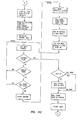
- FIGURES llA, 11B, and 11C detail a functional flowchart of the software executed by the microprocessor of the present invention.
- the essential function of the microprocessor is to access and read the optical random access memory and to provide an output to either an operator display or a host computer as to the edge locations of the work pieces in a work station.
- the function is that of determining which of the fibers within a line have been exposed to light and which have not in order to locate the edge of the work piece on each of the arrays on the work station surface that have been optically coupled to the optical RAM through the optical fibers as previously discussed.
- the microprocessor used in the present invention is required to perform a convention calibration to determine the appropriate exposure time.
- Another functional requirement to be performed by the microprocessor is that of determining when a true edge has been detected. This requirement is present because the work pieces involved in the specific application of this invention are pieces of cloth whose edges may be frayed or contain lint. Therefore, the microprocessor also performs a conventional algorithm to determine, if in fact, the edge detected is in fact the true edge.
- the microprocessor begins execution at the start position after either a reset signal is received or after power up.
- the first function accomplished is the initialization of the Input/Output ports.
- the executed software initializes the serial Input/Output ports for communications with the host computer.
- this invention may or may not be used with a host computer. In an embodiment employing a host computer, this computer would perform a robotic function based upon the positional information provided by the invention. However, this invention may be used without a host computer to display positional data to an operator on an operator display.
- the software determines which cameras the invention is to access and what mode the invention is to operate in by reading externally set switches.
- the invention may operate off a single scan line from eight separate cameras or, alternatively, operate eight scan lines of a single camera.
- a single camera is used to read eight lines that are provided to the camera en closure.
- the control words used to determine the camera and mode operations are "CAMSW" and "MISCSW". The software then clears all the optical RAM memory locations.
- the auto-white calibration algorithm (setting exposure time) is next performed and involves the scanning of the memory elements representing pixels to determine if they are all white after they have been refreshed and all exposed to light.
- This calibration algorithm starts at the maximum value that has been set by a constant in software, which in the preferred embodiment is approximately 100 milliseconds.
- the auto-white calibration algorithm all pixels of the line are scanned. If all pixels have discharged, the exposure time is decreased. This operation continues until at least one pixel does not transition. Then the exposure time is increased by approximately eight percent. It should be understood that the auto-white calibration sequence is performed when all the scan lines are exposed to light.
- the auto-white calibration sequence is illustrated in FIGURE llA as including the NXTCAM, AUTOLIN, and WHSEEK subroutines as illustrated.
- the auto-white sequence is exited along the LEDSON line as shown wherein the LED's an the operator display are turned on.
- the software enters the idle loop at 2A wherein the 1 second timer is tested and if the 1 second timer has timed out, the timer is restarted and all the camera scan lines are refreshed. If the 1 second timer is not timed out, these steps are skipped and then the test switch is read to determine if a request is present. If a request is present, the presence of this request signifies that there is no host computer connected and the operation of the invention and the microprocessor software is performed providing output data only to the operator display and not to the communications port. If the test switch request line is not present, then, conversely, there is a host computer present and communications must be established during the first loop as shown by the next decision step.
- This next step determines if the host has sent an "A" which is to be acknowledged by the microprocessor.
- the A command by protocol is the first command from the host to establish communication with the microprocessor. If a message has not been received, then the software loops through the idle loop again. Upon the second time through, again, the host message is examined. The software will remain in a loop until a message has been received. If the message received is a "D” then the sequence is started. However, if neither the "A" command of the "D” command are not received at the appropriate times, a no acknowledge "NAK" is sent to the host via the communications port.
- the software then executes along the GO line as shown in FIGURE 11B by first loading all edge answer registers with "FF" (hexidecimal).
- the "FF" is the default condition for the registers, i.e. all "l's”.
- the camera switch "CAMSW” and mode switch “MISCSW” are then read and a camera scan is next initialized. Each of the scan lines of the cameras are then "individually read as shown. If all the lines are white or black, the next camera or camera scan line is read. If the lines contain both black and white information then the edge is determined.
- the algorithm for determining the edge determines which pixel location has transitioned and then reads the next 20 pixels.
- the new transition point is stored and then the next 20 pixels are read. This process continues until 20 pixels are read without an additional transition.
- This 20 pixel overscan technique is included to determine if the proper edge has been detected and not merely a piece of thread or a piece of lint. Additionally, this same loop will provide an average if a mode is selected that includes 4 scan lines located at each array location on the work station. In other words, instead of a single line of fibers, 4 lines of fibers are located parallel to each other and the 4 lines in the camera are each individually addressed to determine where the edge is for that line. The edge data for the 4 lines is then averaged to provide the edge location.
- the edge line information is provided for determining the location, position and orientation of a work piece on the work place or work surface.
- the preferred embodiments described above utilize optical fibers to receive the light and transmit it to an optical RAM.
- the present invention also includes the use of photocells or other light receiving devices which can generate electrical signals directly for interacting with a conventional random access memory in accordance with the present invention. It is expected that the claims of the present application cover this variation.
Landscapes
- Physics & Mathematics (AREA)
- General Physics & Mathematics (AREA)
- Life Sciences & Earth Sciences (AREA)
- General Life Sciences & Earth Sciences (AREA)
- Geophysics (AREA)
- Length Measuring Devices By Optical Means (AREA)
- Geophysics And Detection Of Objects (AREA)
- Mechanical Coupling Of Light Guides (AREA)
- Optical Transform (AREA)
Abstract
Description
- objects.
- A common technique used by these prior art vision systems is to take an N by M array representing the pixel elements of a view of the object and produce data representing this N by M array for analysis by a computer. As should be appreciated by those skilled in the art, such an analysis usually requires extensive computer resources and time to complete the analysis. Therefore, the use of vision systems in real time computer operations for support of manufacturing processing has,been limited.
- One early attempt to solve this problem is disclosed in U.S. Patent No. 4,105,925 entitled "Optical Object Locator" which discloses a device for determining the position and orientation of an object on a conveyor by the use of two planes of light that intersect in a single transverse line on a conveyor surface. A linear diode array that is aligned along the single line of light on the conveyor detects light from that line by electronic sampling of the lumination of this linear array. Object boundaries are determined and object shape and orientation may thus be determined. Another patent entitled "Light Collection Apparatus" disclosed in U.S. Patent No. 3,987,301 discloses an apparatus for detecting the presence of extraneous matter and/or _ cracks in translucent containers. The light collection apparatus incorporates an array of fiber optics elements arranged to perform an accurate and controllable method of light collection.
- A further attempt at solving this problem is disclosed in "Device for Detecting the Position of Web Side
- This invention relates to automated vision systems for manufacturing and more particularly to a vision system for determining article positions during a manufacturing process.
- Recently there has been increased interest in machine vision devices for industrial applications. This increased interest is attributed to the increased research in computer technology. Usually, the first step in vision analysis by a machine vision device is the conversion of analog pixel (picture element) data into digital data for processing by a computer. Historically, several different types of devices have been used. Most commonly used in early applications were the vidicon video tube cameras that ·produced analog video signals. More recently solid state cameras or cameras using charge-coupled devices (CCD) have been used. The use of the vidicon cameras and the solid state cameras is discussed in Chapter 2 of Machine Vision for Robotics and Automated Inspection, Vol. I - Fundamentals, by Richard K. Miller, published by Technical Insights, Inc. which is herein incorporated by reference.
Chapter 4 entitled "Model Machine Vision Systems" and Chapter 9 entitled "General Methods to Enable Robots with Vision to Acquire, Orient and Transport Work Pieces" of this publication disclose different techniques used in the prior art to detect and determine the position of different Edge" in U.S. Patent No. 4,146,797 which includes a single light emitting source, a lens to form a beam of light in the vicinity of a reference point and an optical fiber to transmit the light to a photoelectric converter. The output of the photoelectric converter is used to determine when the edge of the web has been detected. - The present invention has been embodied in an apparatus to provide vision information for a manufacturing environment. An object of the present invention is to provide a non-complex vision system that indicates the location and positioning of an article used in manufacture.
- A further object of the present invention is to provide a vision apparatus that provides a digital output without having to perform analog to digital data conversions.
- A further object of the present invention is to provide a vision apparatus that allows variations in optical resolution.
- In accordance with the present invention a vision apparatus for detecting the presence of an object as the object passes across a lighted surface is provided. At least one light receiving array is located on the surface of a path traveled by an object. This light receiving array includes a light transfer device for conducting light radiated upon the light receiving array to an optical sensor. The optical sensor produces an electrical signal indicating what portion of the light receiving array is receiving light.
- In one embodiment of the present invention the apparatus includes several linear arrays located upon the surface of a work station. Articles of manufacture pass across this surface and over these arrays. Specifically, the apparatus includes several linear arrays of optical fibers positioned such that one end of each of the optical fibers receives light along the surface of this work station area. The other ends of the optical fiber arrays are connected to a fixed matrix plate which is positioned in a camera enclosure to emit light through a lens system onto an optical sensor. In this embodiment, the optical sensor is a random access memory which is continually read by a computational device to determine what portions of the random access memory device have been exposed to light.
- Still further in this embodiment, the individual optical fibers are collimated to emit light upon specific elements of the optical random access memory. Therefore, the illumination of a specific element of the random access memory directly correlates to the illumination of the location of that fiber element end upon the work station surface. The output from the memory is digital data indicating the edge locations of the articles upon the work station surface.
- In another embodiment of the present invention several linear arrays of the optical fibers are arranged at the work station in an orthogonal and three dimensional relationship. Additionally, the spacing between the fibers ends at the work station is different than the fiber end spacing at the camera enclosure end of the fiber optical fiber bundle. By varying the distance between the optical fibers at the work station end, the resolution of the visi-ca system can be effectively varied.
- The novel features believed characteristic of the invention are set forth in the appended claims. The invention itself, however, as well as a preferred mode of use will best be understood by reference to the following detailed description of an illustrative embodiment when read in conjunction with the accompanying drawings, wherein:
- FIGURE 1 is a top view of a work station surface including the ends of optical fiber bundles comprising six linear optical fiber arrays in accordance with a preferred embodiment of the present invention;
- FIGURE 2 is a symbolic view of a single bundle of optical fibers forming a single linear arrays of FIGURE 1 positioned to illuminate an optical random access memory;
- FIGURE 3 is a symbolic view of the array and memory of the embodiment of Figure 2 depicting the illumination of the optical random access memory when a article of manufacture is blocking part of the light transferred to the linear optical fiber array;
- FIGURE 4 is a symbolic showing the relative locations of the optical fiber bundles, linear arrays, the work station surface, the lensing mechanism and the optical random access memory of the embodiment of FIGURES 1-3;
- FIGURE 5 is an exploded view of a camera enclosure for the optical fiber arrays, the lens and the optical random access memory of the embodiment shown in FIGURES 1-4;
- FIGURE 6 is an isometric view of a cylinder used to position the optical fiber bundles shown in FIGURE 4 to form a linear array;
- FIGURE 7 is a longitudinal cross-sectional view of the cylinder of FIGURE 6;
- FIGURE 8 illustrates the fiber illumination of the individual pixel elements of the optical random access memory shown in FIGURES 2-5;
- FIGURE 9 is a top' view of a work station in accordance with another embodiment of the present invention having four linear arrays per work piece to determine the location and orientation of the work piece;
- FIGURE 10 is an illustration of a work station in accordance with another embodiment of the present invention including three dimensional orthogonally positioned linear arrays for detecting the location and position of a three dimensional work piece; and
- FIGURES 11A., B, and C are flowcharts for the software used to access data from the optical random access memory shown in FIGURES 2-5.
- In the preferred embodiment, this invention is applied to a work place for manufacturing articles of clothing. The articles of manufacture are cloth material which are essentially two dimensional in nature. However, it should be understood, that this invention is also capable of detecting the positional orientation of an article having three dimensions. The purpose of this invention is to provide digital data indicating the edge locations of these articles. For articles of known shapes and dimensions, an attached computer can determine the center of the article and-further can direct a robotic arm to the article to pickup the article wherein the article will be grasped in a known orientation.
- FIGURE 1 illustrates a
work place 10 containing two articles ofmanufacture 12 and 14. In the preferred embodiment these articles ofmanufacture 12 and 14 represent pockets for denim blue jeans: The object of the invention is to provide data representing the positional orientation of thesepockets 12 and 14. , Thework station 10 includes severallinear arrays optical fiber ribbon 28 having a linear arrangement of optical fiber ends, as shown in FIGURE 2. -When thepockets 12 and 14 are positioned over these linear arrays, light is blocked from illuminating the optical fibers underneath the pockets. - FIGURE 2 illustrates a symbolic view of the
linear array 16 including thelinear ribbon 28 of optical fiber ends. The optical fibers oflinear array 16 are contained within anoptical fiber bundle 30 which terminates in a secondlinear array 34 exposing the opposite ends of the optical fibers to provide anoptical fiber ribbon 32. Theribbon 32 is optically coupled as illustrated by field of view 36 through alens 40 to anoptical RAM 42 that is contained within acamera enclosure 38. In the preferred embodiment, thelinear array 34 is positioned on one end of thecamera enclosure 38. The purpose of thecamera enclosure 38 is to minimize the amount of extaneous light to theoptical RAM 42. Theoptical RAM 42 provides binary data onlines 44 to indicate which of the fibers are receiving light. - In FIGURE 2, the length of
ribbon 28 appears to be similar to the length ofribbon 32. In the preferred embodiment, bundle 30 consists of 256 optical fibers that terminate in aoptical fiber ribbon 32 that is 2.56 inches in width.Ribbon 28, which is the work station end ofbundle 30, is also 2.56 inches wide (i.e., 100 fibers per inch). However, by varying the spacing of the optical fibers in the work station, the apparent resolution of the optical fiber system can be changed, even though the appearance of the fiber ribbons at the camera enclosure always remain the same. - FIGURE 3 schematically illustrates the illumination of a portion of an
optical fiber ribbon 28. Theoptical fiber ribbon 28 includes alength 45 of which onlyportion 46 receives light. Since theoptical ribbon 28 is located in the surface ofwork place 10, light above the work place surface irradiating down upon the work space surface is blocked by work piece 12 from all butportion 46 of theoptical fiber ribbon 28. As a result, only aportion 48 of theoptical RAM 42 is illuminated through thelensing system 40. This action indicates one edge of the work piece 12. In a similar manner the other edges of the work piece are located. Thus, by using the three optical fiber ribbons of thearrays work space 10 is determined. - FIGURE 4 illustrates the coupling of the optical system of a preferred embodiment of the present invention. Specifically, a
work space 100 includes 6linear arrays Work pieces 102 and 104 are illustrated at a position above the linear arrays as the work pieces travel acrosswork space 100. Each of the linear arrays 106-116 are coupled to anoptical fiber bundle 118 that terminates in anarray matrix 120. Thematrix 120 includes several linear optical fiber ribbons- 121-126, shown in Figure 5, corresponding to each of the linear arrays 106-116 ofwork place 100. Alens 132 provides a field ofview 128 to transfer light from thearray matrix 120 to an opticalrandom access memory 134. - FIGURE 5 more clearly illustrates the linear ribbons 121-126 within the
array matrix 120 which is, in FIGURE 5, exploded from the left most end of thecamera enclosure 130. It should be appreciated that thecamera enclosure 130 is a light sealed structure that enables only the light from the linear ribbons 121-126 to enter the interior portion of thelight enclosure 130 and illuminate the surface of theoptical RAM 134. - FIGURE 6 illustrates a
cylinder 140 used to assemble the linear optical fiber ribbons 121-126.Cylinder 140 includes two relatively largecircumferential grooves circumferential grooves 144. Thelarger grooves grooves 144 as light transmitting fibers. Alongitudinal channel 145 is provided along a portion of the perphery ofcylinder 140 to receive a mold (not shown). When the fibers are in place ingrooves channel 145 underneath and above the fibers ingrooves grooves cylinder 140. The mold is then removed from the optical fiber ribbon assembly and the ends of this ribbon assembly are appropriately machined and surfaced by conventional means to permit reception or emission of light. The epoxied fiber bundle is then assembled in a linear array structure at the work place or at the matrix plate, the reference fibers which were ingrooves grooves 144. - In an alternative- embodiment, the
matrix plate 120 of FIGURE 5 is replaced by a solid plate that includes selectively drilled holes to receive individual optical fibers. Once these fibers have been assembled in their respective holes, the optical fiber bundle is sealed and fixed to thematrix plate 120 in a conventional manner that will not interfere with the light transmissivity property of the individual fibers. - FIGURE 7 illustrates a longitudinal cross-sectional view of
cylinder 140 of FIGURE 6 showing the optical fiber arrangement.Reference fibers respective grooves optical fibers fibers 153 lie in spaced apartgrooves 144. Eightfibers 154 are each positioned between two offibers 153 on ridges 156. The purpose for this configuration of optical fibers is explained by reference to FIGURE 8. - FIGURE 8 illustrates one aspect of a preferred embodiment of the optical
random acess memory 134.Optical memory elements 160 are positioned in two rows upon the surface of the opticalrandom access memory 134. The specific topology of opticalrandom access memory 134 requires that a linear optical fiber array such as that of FIGURE 7 illuminatecircular portions memory elements 160. This illumination occurs by focusing individual light elements ontoportions particular memory element 160 will cause the capacitor of that element which is initially precharged to discharge. Thus initially, the optical random access memory elements exposed to light are refreshed, as in a conventional computer dynamic random access memory. The remaining elements not exposed to light maintain their charged state. - To access the data in the optical random access memory, the memory is addressed by column and row in a conventional fashion. As those skilled in the art can appreciate, the positioning of the
optical fibers memory elements 160 in FIGURE 8. Typically, the spacing 166 between the illumination ofarea - In a preferred embodiment the
height 170 of amemory cell 160 is 4 x 10⁻³ inches and the width of eachcell 160 is about 5 x 10⁻³ inches. The illumination of these elements is provided from optical fibers that are 10 mills in diameter. In this preferred embodiment the optical random access memory requiring such a focusing arrangement is the IS32 Optical RAM by Micron Technology of Boise, Idaho. The camera lens is preferably a 16mm lens having an F stop of 1:1.4. The aperture of the lens is opened to 1.4. - The lens is preferably positioned as shown in FIGURE 5 between the surface of
optical RAM 134 containing and thematrix array 120, to focus each fiber optic end upon a respective one of the random access memory elements, as shown in FIGURE 8. - FIGURE 9 illustrates another embodiment of the present invention having four
linear arrays work station 200 to determine the center ofwork piece 210. Yet another embodiment of the present invention is shown in FIGURE 10.Linear arrays - In a preferred embodiment, the optical
random access memory 134 is connected to a microprocessor (not shown), preferably a Motorola model 68701, which provides dynamic refresh in scanning the data of the optical RAM. - This microprocessor also provides data to an external host computer concerning the location of the work piece being processed. This is accomplished through a serial RS-232 communications port or by a parallel port. When not accessing the data, the microprocessor provides refresh signals to the random access memory.
- FIGURES llA, 11B, and 11C detail a functional flowchart of the software executed by the microprocessor of the present invention. It should be understood that the essential function of the microprocessor is to access and read the optical random access memory and to provide an output to either an operator display or a host computer as to the edge locations of the work pieces in a work station. Generally speaking, the function is that of determining which of the fibers within a line have been exposed to light and which have not in order to locate the edge of the work piece on each of the arrays on the work station surface that have been optically coupled to the optical RAM through the optical fibers as previously discussed.
- The use of the IS32 OPTIC RAM™ by Micron Technology, Inc. requires the microprocessor of this invention to perform not only the read task but to perform what is termed "setting the exposure time". Simply, the operation of this optical RAM requires that the RAM locations receive a "1" and then after some time, to be termed "exposure time", the RAM is read. This optical RAM is configured so that the individual memory elements that have been exposed to light will lose their charge, i.e. these elements will transition from the "1" to a "0" stored value. As those skilled in the art should appreciate, if the time between the writing of a "1" and the reading of the memory contents is too long, all the memory elements will discharge whether they are exposed to light or not. However, if this time between the write operation and read operation is too short, all the memory elements would still be l's even if they were exposed to light, i.e. they had not had enough time to be discharged. Therefore, the microprocessor used in the present invention is required to perform a convention calibration to determine the appropriate exposure time.
- Another functional requirement to be performed by the microprocessor is that of determining when a true edge has been detected. This requirement is present because the work pieces involved in the specific application of this invention are pieces of cloth whose edges may be frayed or contain lint. Therefore, the microprocessor also performs a conventional algorithm to determine, if in fact, the edge detected is in fact the true edge.
- Referring to FIGURE llA, the microprocessor begins execution at the start position after either a reset signal is received or after power up. The first function accomplished is the initialization of the Input/Output ports. _Next, the executed software initializes the serial Input/Output ports for communications with the host computer. As previously explained, this invention may or may not be used with a host computer. In an embodiment employing a host computer, this computer would perform a robotic function based upon the positional information provided by the invention. However, this invention may be used without a host computer to display positional data to an operator on an operator display.
- Next, the software determines which cameras the invention is to access and what mode the invention is to operate in by reading externally set switches. Specifically, the invention may operate off a single scan line from eight separate cameras or, alternatively, operate eight scan lines of a single camera. In the preferred embodiment, a single camera is used to read eight lines that are provided to the camera en closure. Specifically, the control words used to determine the camera and mode operations are "CAMSW" and "MISCSW". The software then clears all the optical RAM memory locations.
- The auto-white calibration algorithm (setting exposure time) is next performed and involves the scanning of the memory elements representing pixels to determine if they are all white after they have been refreshed and all exposed to light. This calibration algorithm starts at the maximum value that has been set by a constant in software, which in the preferred embodiment is approximately 100 milliseconds. According to the auto-white calibration algorithm, all pixels of the line are scanned. If all pixels have discharged, the exposure time is decreased. This operation continues until at least one pixel does not transition. Then the exposure time is increased by approximately eight percent. It should be understood that the auto-white calibration sequence is performed when all the scan lines are exposed to light.
- The auto-white calibration sequence is illustrated in FIGURE llA as including the NXTCAM, AUTOLIN, and WHSEEK subroutines as illustrated. The auto-white sequence is exited along the LEDSON line as shown wherein the LED's an the operator display are turned on.
- Referring to FIGURE llB, the software enters the idle loop at 2A wherein the 1 second timer is tested and if the 1 second timer has timed out, the timer is restarted and all the camera scan lines are refreshed. If the 1 second timer is not timed out, these steps are skipped and then the test switch is read to determine if a request is present. If a request is present, the presence of this request signifies that there is no host computer connected and the operation of the invention and the microprocessor software is performed providing output data only to the operator display and not to the communications port. If the test switch request line is not present, then, conversely, there is a host computer present and communications must be established during the first loop as shown by the next decision step. This next step determines if the host has sent an "A" which is to be acknowledged by the microprocessor. The A command by protocol is the first command from the host to establish communication with the microprocessor. If a message has not been received, then the software loops through the idle loop again. Upon the second time through, again, the host message is examined. The software will remain in a loop until a message has been received. If the message received is a "D" then the sequence is started. However, if neither the "A" command of the "D" command are not received at the appropriate times, a no acknowledge "NAK" is sent to the host via the communications port.
- Given that all the communications with the host are properly established, the software then executes along the GO line as shown in FIGURE 11B by first loading all edge answer registers with "FF" (hexidecimal). The "FF" is the default condition for the registers, i.e. all "l's". The camera switch "CAMSW" and mode switch "MISCSW" are then read and a camera scan is next initialized. Each of the scan lines of the cameras are then "individually read as shown. If all the lines are white or black, the next camera or camera scan line is read. If the lines contain both black and white information then the edge is determined. The algorithm for determining the edge determines which pixel location has transitioned and then reads the next 20 pixels. If there is an additional transition within the next 20 pixels, the new transition point is stored and then the next 20 pixels are read. This process continues until 20 pixels are read without an additional transition. This 20 pixel overscan technique is included to determine if the proper edge has been detected and not merely a piece of thread or a piece of lint. Additionally, this same loop will provide an average if a mode is selected that includes 4 scan lines located at each array location on the work station. In other words, instead of a single line of fibers, 4 lines of fibers are located parallel to each other and the 4 lines in the camera are each individually addressed to determine where the edge is for that line. The edge data for the 4 lines is then averaged to provide the edge location.
- After all the camera lines have been scanned, the results are output to the operator display and, if a host computer is present, this information is provided to the host through the communications port. The software then loops back to node 2B which is illustrated in FIGURE llB.
- By operating in this manner, the edge line information is provided for determining the location, position and orientation of a work piece on the work place or work surface.
- The preferred embodiments described above utilize optical fibers to receive the light and transmit it to an optical RAM. However, it is understood that the present invention also includes the use of photocells or other light receiving devices which can generate electrical signals directly for interacting with a conventional random access memory in accordance with the present invention. It is expected that the claims of the present application cover this variation.
- Although the invention has been described with reference to specific embodiments, this description is not meant to be construed in a limiting sense. Various modifications of the disclosed embodiments as well as other alternative embodiments of the invention will become apparent to persons skilled in the art upon reference to the description of the invention. It is therefore contemplated that the appended claims will cover any such modifications or embodiments that fall within the true scope of the invention.
Claims (23)
Priority Applications (1)
| Application Number | Priority Date | Filing Date | Title |
|---|---|---|---|
| AT86116651T ATE72903T1 (en) | 1985-12-05 | 1986-12-01 | HIGH RESOLUTION OPTICAL FIBER ARRAY AND OBJECT POSITIONING SYSTEM. |
Applications Claiming Priority (2)
| Application Number | Priority Date | Filing Date | Title |
|---|---|---|---|
| US80527185A | 1985-12-05 | 1985-12-05 | |
| US805271 | 2007-05-21 |
Publications (3)
| Publication Number | Publication Date |
|---|---|
| EP0224901A2 true EP0224901A2 (en) | 1987-06-10 |
| EP0224901A3 EP0224901A3 (en) | 1989-06-14 |
| EP0224901B1 EP0224901B1 (en) | 1992-02-26 |
Family
ID=25191104
Family Applications (1)
| Application Number | Title | Priority Date | Filing Date |
|---|---|---|---|
| EP86116651A Expired EP0224901B1 (en) | 1985-12-05 | 1986-12-01 | High resolution optical fiber array and article position determining system |
Country Status (5)
| Country | Link |
|---|---|
| US (1) | US4795913A (en) |
| EP (1) | EP0224901B1 (en) |
| JP (1) | JPH0684885B2 (en) |
| AT (1) | ATE72903T1 (en) |
| DE (1) | DE3683991D1 (en) |
Cited By (1)
| Publication number | Priority date | Publication date | Assignee | Title |
|---|---|---|---|---|
| FR2675574A1 (en) * | 1991-04-22 | 1992-10-23 | Merlin Gerin | OPTICAL PICKUP DEVICE CAPABLE OF PROVIDING REPRESENTATIVE INFORMATION OF A SURFACE CONDITION. |
Families Citing this family (13)
| Publication number | Priority date | Publication date | Assignee | Title |
|---|---|---|---|---|
| US4891528A (en) * | 1989-03-23 | 1990-01-02 | Crosfield Ebway, Inc. | Microprocessor-controlled apparatus for detecting and guiding a web wherein right and left eyespots are formed to determine right and left edges |
| US5003189A (en) * | 1989-10-10 | 1991-03-26 | Unisys Corp. | Document-imaging illumination with fibre-optic intensity-adjust |
| US5089713A (en) * | 1989-10-10 | 1992-02-18 | Unisys Corporation | Document-imaging illumination arrangements with intensity with adjustment |
| US4980971A (en) * | 1989-12-14 | 1991-01-01 | At&T Bell Laboratories | Method and apparatus for chip placement |
| US5324934A (en) * | 1991-05-01 | 1994-06-28 | Megamation Incorporated | Fiberoptic encoder for linear motors and the like |
| US5790687A (en) * | 1996-06-18 | 1998-08-04 | Levi Strauss & Co. | Method and apparatus for the optical determination of the orientation of a garment workpiece |
| US6222623B1 (en) | 1999-09-03 | 2001-04-24 | Mars Incorporated | Integrating light mixer |
| FR2851341B1 (en) * | 2003-02-14 | 2005-04-22 | Etude Et Realisation Electroni | SYSTEM FOR OPTICALLY DETECTING OBJECTS OR PEOPLE |
| US20110175997A1 (en) * | 2008-01-23 | 2011-07-21 | Cyberoptics Corporation | High speed optical inspection system with multiple illumination imagery |
| US8872912B2 (en) * | 2009-09-22 | 2014-10-28 | Cyberoptics Corporation | High speed distributed optical sensor inspection system |
| US8670031B2 (en) * | 2009-09-22 | 2014-03-11 | Cyberoptics Corporation | High speed optical inspection system with camera array and compact, integrated illuminator |
| US8681211B2 (en) * | 2009-09-22 | 2014-03-25 | Cyberoptics Corporation | High speed optical inspection system with adaptive focusing |
| US8894259B2 (en) * | 2009-09-22 | 2014-11-25 | Cyberoptics Corporation | Dark field illuminator with large working area |
Citations (5)
| Publication number | Priority date | Publication date | Assignee | Title |
|---|---|---|---|---|
| DE1448394A1 (en) * | 1963-03-13 | 1969-02-06 | Davy And United Instr Ltd | Position and length measuring device |
| US3761723A (en) * | 1970-06-29 | 1973-09-25 | Agfa Gevaert Nv | Apparatus for measuring dimensional deviations |
| US4146797A (en) * | 1976-12-30 | 1979-03-27 | Tokyo Kikai Seisakusho, Ltd. | Device for detecting the position of web side edge |
| JPS6086678A (en) * | 1983-10-18 | 1985-05-16 | Comput Services Corp | Reader of optical storage card |
| FR2565216A1 (en) * | 1984-06-05 | 1985-12-06 | Leguisquet Loic | Optoelectronic device for the accurate lateral inspection of the unwinding of a web of material such as paper |
Family Cites Families (15)
| Publication number | Priority date | Publication date | Assignee | Title |
|---|---|---|---|---|
| US3104191A (en) * | 1957-12-19 | 1963-09-17 | American Optical Corp | Method of manufacturing optical image transfer devices |
| US3072081A (en) * | 1960-04-05 | 1963-01-08 | Cluett Peabody & Co Inc | Edge guide automatic sewing |
| US3430057A (en) * | 1965-06-22 | 1969-02-25 | Schneider Co Optische Werke | Episcopic scanning head having smaller optical fibers interleaved in interstices formed by contiguous larger fibers |
| JPS4823460B1 (en) * | 1968-11-18 | 1973-07-13 | ||
| US3727567A (en) * | 1969-08-19 | 1973-04-17 | Farah Mfg Co Inc | Automatic sewing apparatus |
| US3609373A (en) * | 1970-05-18 | 1971-09-28 | Singer Co | Photoelectric sensors and circuitry for edge-guiding systems for sewing machines |
| US3987301A (en) * | 1973-06-27 | 1976-10-19 | Talcoma Teoranta | Light collection apparatus |
| US3867889A (en) * | 1973-08-03 | 1975-02-25 | Stahl Urban Co | Apparatus for seaming pieces of textile fabric or the like |
| JPS51107154A (en) * | 1975-03-18 | 1976-09-22 | Hiroaki Oikawa | TEREBIKAMERANYOTSUTE DOJINIFUKUSUKASHONO SOKUCHOOOKONAUHOHO |
| US4105925A (en) * | 1977-03-14 | 1978-08-08 | General Motors Corporation | Optical object locator |
| US4149091A (en) * | 1977-05-02 | 1979-04-10 | Xerox Corporation | Scanning apparatus |
| DE3016676C2 (en) * | 1980-04-30 | 1982-06-16 | Pfaff Industriemaschinen Gmbh, 6750 Kaiserslautern | Automatic sewing system for sewing two material systems together at the same edge |
| JPS5895707A (en) * | 1981-12-02 | 1983-06-07 | Olympus Optical Co Ltd | Automatic focus detecting mechanism of endoscope |
| JPS6098380A (en) * | 1983-11-02 | 1985-06-01 | Dowa Mining Co Ltd | Optical position detector |
| JPS60192905A (en) * | 1984-03-13 | 1985-10-01 | Sharp Corp | Mark detecting device |
-
1986
- 1986-12-01 EP EP86116651A patent/EP0224901B1/en not_active Expired
- 1986-12-01 DE DE8686116651T patent/DE3683991D1/en not_active Expired - Lifetime
- 1986-12-01 AT AT86116651T patent/ATE72903T1/en not_active IP Right Cessation
- 1986-12-03 JP JP61288628A patent/JPH0684885B2/en not_active Expired - Lifetime
-
1987
- 1987-08-06 US US07/083,902 patent/US4795913A/en not_active Expired - Lifetime
Patent Citations (5)
| Publication number | Priority date | Publication date | Assignee | Title |
|---|---|---|---|---|
| DE1448394A1 (en) * | 1963-03-13 | 1969-02-06 | Davy And United Instr Ltd | Position and length measuring device |
| US3761723A (en) * | 1970-06-29 | 1973-09-25 | Agfa Gevaert Nv | Apparatus for measuring dimensional deviations |
| US4146797A (en) * | 1976-12-30 | 1979-03-27 | Tokyo Kikai Seisakusho, Ltd. | Device for detecting the position of web side edge |
| JPS6086678A (en) * | 1983-10-18 | 1985-05-16 | Comput Services Corp | Reader of optical storage card |
| FR2565216A1 (en) * | 1984-06-05 | 1985-12-06 | Leguisquet Loic | Optoelectronic device for the accurate lateral inspection of the unwinding of a web of material such as paper |
Non-Patent Citations (1)
| Title |
|---|
| PATENT ABSTRACTS OF JAPAN, vol. 9, no. 232 (P-389)[1955], 18th September 1985; & JP-A-60 086 678 (KONPIYUUTAA SERVICE K.K.) 16-05-1985 * |
Cited By (2)
| Publication number | Priority date | Publication date | Assignee | Title |
|---|---|---|---|---|
| FR2675574A1 (en) * | 1991-04-22 | 1992-10-23 | Merlin Gerin | OPTICAL PICKUP DEVICE CAPABLE OF PROVIDING REPRESENTATIVE INFORMATION OF A SURFACE CONDITION. |
| EP0511122A1 (en) * | 1991-04-22 | 1992-10-28 | Schneider Electric Sa | Optical transducer suitable to provide information representative of the state of a surface |
Also Published As
| Publication number | Publication date |
|---|---|
| JPH0684885B2 (en) | 1994-10-26 |
| EP0224901A3 (en) | 1989-06-14 |
| JPS62134504A (en) | 1987-06-17 |
| DE3683991D1 (en) | 1992-04-02 |
| ATE72903T1 (en) | 1992-03-15 |
| EP0224901B1 (en) | 1992-02-26 |
| US4795913A (en) | 1989-01-03 |
Similar Documents
| Publication | Publication Date | Title |
|---|---|---|
| EP0224901B1 (en) | High resolution optical fiber array and article position determining system | |
| US4818886A (en) | Method and apparatus for self-referencing and self-focusing a bar-code reader | |
| US5633487A (en) | Multi-focal vision system | |
| US4611292A (en) | Robot vision system | |
| EP0944237B1 (en) | Portable image scanner with optical position sensors | |
| US4958223A (en) | Inspection of container finish | |
| JPH10332320A (en) | Product scanning device and method | |
| US4772128A (en) | Fiber optic imaging system for on-line monitoring | |
| IE41977B1 (en) | Improvements in or relating to a system for remotely identifying objects bearing coded information | |
| CA2402632A1 (en) | Imaging system | |
| WO2002040383A2 (en) | Method and apparatus for the automated inspection of yarn packages | |
| KR20010034488A (en) | System and method for selective scanning of an object or pattern including scan correction | |
| JPH02110356A (en) | Defect detecting apparatus using linear light source | |
| JPH02105041A (en) | Particle measuring instrument | |
| US20020148944A1 (en) | Laser optical area scanner and response system and methods | |
| CA1315390C (en) | Inspection of container finish | |
| EP1381881B1 (en) | System and method for optically sensing motion of objects | |
| US6734981B1 (en) | Multiple laser optical systems and methods | |
| EP0935135A1 (en) | System for measuring solder bumps | |
| EP0606770B1 (en) | A measuring-point member for optical measurement | |
| KR102539714B1 (en) | Apparatus for secondary battery appearance inspection | |
| EP4269989A1 (en) | Apparatus for inspecting appearance of secondary battery | |
| JPS6353537A (en) | Lighting device | |
| WO2000040957A1 (en) | Method and device for measuring labels in a carrier | |
| JPS63302349A (en) | Apparatus of inspecting pattern |
Legal Events
| Date | Code | Title | Description |
|---|---|---|---|
| PUAI | Public reference made under article 153(3) epc to a published international application that has entered the european phase |
Free format text: ORIGINAL CODE: 0009012 |
|
| 17P | Request for examination filed |
Effective date: 19861201 |
|
| AK | Designated contracting states |
Kind code of ref document: A2 Designated state(s): AT BE CH DE ES FR GB GR IT LI LU NL SE |
|
| PUAL | Search report despatched |
Free format text: ORIGINAL CODE: 0009013 |
|
| AK | Designated contracting states |
Kind code of ref document: A3 Designated state(s): AT BE CH DE ES FR GB GR IT LI LU NL SE |
|
| 17Q | First examination report despatched |
Effective date: 19900620 |
|
| GRAA | (expected) grant |
Free format text: ORIGINAL CODE: 0009210 |
|
| AK | Designated contracting states |
Kind code of ref document: B1 Designated state(s): AT BE CH DE ES FR GB GR IT LI LU NL SE |
|
| PG25 | Lapsed in a contracting state [announced via postgrant information from national office to epo] |
Ref country code: SE Effective date: 19920226 Ref country code: NL Effective date: 19920226 Ref country code: LI Effective date: 19920226 Ref country code: GR Free format text: LAPSE BECAUSE OF FAILURE TO SUBMIT A TRANSLATION OF THE DESCRIPTION OR TO PAY THE FEE WITHIN THE PRESCRIBED TIME-LIMIT Effective date: 19920226 Ref country code: CH Effective date: 19920226 Ref country code: AT Effective date: 19920226 |
|
| REF | Corresponds to: |
Ref document number: 72903 Country of ref document: AT Date of ref document: 19920315 Kind code of ref document: T |
|
| ET | Fr: translation filed | ||
| REF | Corresponds to: |
Ref document number: 3683991 Country of ref document: DE Date of ref document: 19920402 |
|
| ITF | It: translation for a ep patent filed | ||
| PG25 | Lapsed in a contracting state [announced via postgrant information from national office to epo] |
Ref country code: ES Free format text: LAPSE BECAUSE OF FAILURE TO SUBMIT A TRANSLATION OF THE DESCRIPTION OR TO PAY THE FEE WITHIN THE PRESCRIBED TIME-LIMIT Effective date: 19920606 |
|
| REG | Reference to a national code |
Ref country code: CH Ref legal event code: PL |
|
| NLV1 | Nl: lapsed or annulled due to failure to fulfill the requirements of art. 29p and 29m of the patents act | ||
| PLBE | No opposition filed within time limit |
Free format text: ORIGINAL CODE: 0009261 |
|
| STAA | Information on the status of an ep patent application or granted ep patent |
Free format text: STATUS: NO OPPOSITION FILED WITHIN TIME LIMIT |
|
| PG25 | Lapsed in a contracting state [announced via postgrant information from national office to epo] |
Ref country code: LU Free format text: LAPSE BECAUSE OF NON-PAYMENT OF DUE FEES Effective date: 19921231 |
|
| 26N | No opposition filed | ||
| ITTA | It: last paid annual fee | ||
| PGFP | Annual fee paid to national office [announced via postgrant information from national office to epo] |
Ref country code: GB Payment date: 20001129 Year of fee payment: 15 Ref country code: DE Payment date: 20001129 Year of fee payment: 15 |
|
| PGFP | Annual fee paid to national office [announced via postgrant information from national office to epo] |
Ref country code: FR Payment date: 20001212 Year of fee payment: 15 |
|
| REG | Reference to a national code |
Ref country code: GB Ref legal event code: 732E |
|
| PG25 | Lapsed in a contracting state [announced via postgrant information from national office to epo] |
Ref country code: GB Free format text: LAPSE BECAUSE OF NON-PAYMENT OF DUE FEES Effective date: 20011201 |
|
| REG | Reference to a national code |
Ref country code: GB Ref legal event code: IF02 |
|
| REG | Reference to a national code |
Ref country code: FR Ref legal event code: GC |
|
| PGFP | Annual fee paid to national office [announced via postgrant information from national office to epo] |
Ref country code: BE Payment date: 20020205 Year of fee payment: 16 |
|
| PG25 | Lapsed in a contracting state [announced via postgrant information from national office to epo] |
Ref country code: DE Free format text: LAPSE BECAUSE OF NON-PAYMENT OF DUE FEES Effective date: 20020702 |
|
| GBPC | Gb: european patent ceased through non-payment of renewal fee |
Effective date: 20011201 |
|
| PG25 | Lapsed in a contracting state [announced via postgrant information from national office to epo] |
Ref country code: FR Free format text: LAPSE BECAUSE OF NON-PAYMENT OF DUE FEES Effective date: 20020830 |
|
| REG | Reference to a national code |
Ref country code: FR Ref legal event code: ST |
|
| PG25 | Lapsed in a contracting state [announced via postgrant information from national office to epo] |
Ref country code: BE Free format text: LAPSE BECAUSE OF NON-PAYMENT OF DUE FEES Effective date: 20021231 |
|
| BERE | Be: lapsed |
Owner name: *LEVI STRAUSS & CO. Effective date: 20021231 |
|
| REG | Reference to a national code |
Ref country code: FR Ref legal event code: DG |
|
| PG25 | Lapsed in a contracting state [announced via postgrant information from national office to epo] |
Ref country code: IT Free format text: LAPSE BECAUSE OF NON-PAYMENT OF DUE FEES;WARNING: LAPSES OF ITALIAN PATENTS WITH EFFECTIVE DATE BEFORE 2007 MAY HAVE OCCURRED AT ANY TIME BEFORE 2007. THE CORRECT EFFECTIVE DATE MAY BE DIFFERENT FROM THE ONE RECORDED. Effective date: 20051201 |